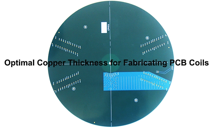
In the realm of design PCB coils are essential components used in a wide range of applications spanning from power electronics to wireless communication systems. The effectiveness of these coils greatly depends on selecting the copper thickness during manufacturing. Taking into account factors like density, skin effect and frequency range allows engineer to pinpoint the ideal copper thickness for their PCB coils. This article aims to explore the importance of copper thickness optimization and provides guidelines, to achieve optimal performance and efficiency in coil fabrication.
Significance of PCB Coils in High-speed Designs
PCB coils play a vital role in high speed designs owing to their inherent capabilities. One such capability is inductance, where coils store energy as a magnetic field. This property is particularly significant in high speed circuits as rapidly switching signals can generate substantial electromagnetic interference. By utilizing coils, unwanted noise and transients can be effectively filtered out, thereby enhancing the overall circuit performance.
In addition coils can be employed to create resonant circuits that can be precisely tuned to specific frequencies. This allows for filtering signals selectively. Enhancing desired frequency elements. These resonant circuits play a role in high speed designs by aiding in accurate signal preparation and guaranteeing top notch performance.
Furthermore, coils are proficient in providing impedance matching functionality. They can be utilized to match the impedance of a source to a load, enabling maximum power transfer and minimizing signal reflections. This aspect holds critical significance in high-speed designs to prevent signal loss and maintain the integrity of the transmitted signals.
Furthermore coils serve as efficient energy storage devices. They have the ability to store and discharge energy when required, which makes them ideal for tasks like filtering power supply and regulating voltage. When coils are integrated into high speed PCBs they guarantee an pure power source for sensitive electronic parts ultimately boosting their dependability and efficiency.
In the realm of high speed PCB, coils find extensive application in various areas. One such area is power supply decoupling, where coils are employed to effectively filter out noise and transients from power supply lines. This ensures a consistent and stable power supply, which is crucial for the optimal functioning of sensitive electronic components.
Furthermore coils are employed in high speed design for signal filtering purposes. They are crucial in removing noise and harmonics from signals, which improves signal quality and reduces electromagnetic interference.
Moreover coils are instrumental in the creation of resonant circuits. When coils are integrated into these circuits they enable selective filtering and impedance matching allowing for accurate signal conditioning and improved overall performance.
Lastly, coils are commonly used as inductors in circuits, like LC filters and voltage regulators. Their inclusion helps improve the efficiency and functionality of these circuits ultimately boosting the performance and dependability of high speed PCB.
In order to achieve the desired inductance, resonance, and impedance matching characteristics, optimizing the copper thickness of PCB coils is of utmost importance. Careful selection of the copper thickness ensure optimal performance, minimizes losses and prevents overheating, thus ensuring the reliable and efficient operation of high speed designs.
Challenges in determining optimal copper thickness
Determining the optimal copper thickness for PCB coils comes with various challenges that engineers need to tackle to ensure the desired performance and reliability. One major issue is dealing with trade offs. When increase the copper thickness, but it usually boosts inductance and lowers resistance. It also makes the coil bigger in size which could make manufacturing more complex. On the side reducing the copper thickness lowers inductance and raises resistance potentially resulting in higher current densities and a greater risk of overheating.
Another challenge lies in the frequency dependence of the optimal copper thickness. The operating frequency of the coil influences this determination. At higher frequencies, the skin effect becomes more pronounced, causing current to flow mainly on the copper surface. Consequently, increasing copper thickness beyond a certain point may not substantially enhance inductance.
Selecting the thickness of copper is made even more difficult by the limitation in manufacturing. The capabilities of manufacturing equipment and the properties of the materials used impose constraint on the minimum and maximum achievable copper thickness. Thinner copper lines are tougher to etch and easier to break, while thicker traces may necessitate additional processing step or specialized equipment.
Thermal management poses another consideration. PCB coils generate heat due to current flow and associated losses. Thicker copper traces exhibit lower resistance and can dissipate heat more efficiently. However, they also possess a larger surface area, potentially requiring supplementary thermal management measures.
In order to determine the copper thickness for a particular PCB coil design engineer need to consider various factor and make decisions based on the specific needs of the application. This usually requires using analytical calculations, simulations and testing to achieve a mix of inductance, resistance, size and ease of manufacturing
Several additional considerations come into play. Coil geometry, including shape, dimensions, number of turns, coil diameter, and spacing between turns, significantly impacts inductance and resistance. The operating power level, which determines the current flowing through the coil, affects temperature rise and the potential for overheating. Additionally, the PCB material, construction type, and the presence of ground planes can influence the coil’s inductance and resistance.
Factors Affecting Copper Thickness Optimization
When optimizing the copper thickness, for PCB coils various aspects need to be taken into account. These elements impact how well the coils function, how easy they are to manufacture and their cost efficiency. By evaluating these factors engineers can make well informed choices to fulfill the precise needs of their projects.
One crucial factor is the shape and size of the coil, like turns quantity, diameter the space between each turn and whether its spiral or rectangular all play a role in determining the coils inductance and resistance.
The operating frequency and power level are other critical considerations. The signals frequency passing through the coil affects its optimal copper thickness. Likewise the current running through the coil plays a role, in determining the power level and how much heat is generated as a result.
Thermal management is a significant concern in PCB coil design. It’s crucial to disperse the heat produced by the coil as a result of current passing through and losses. The ability of the PCB material to conduct heat and its design are factors, in dispersing heat effectively.
Manufacturing capabilities and limitations also shape the choice of copper thickness. Factor such as the range of copper thickness as well as the methods, like etching and plating employed play a significant role. The availability of equipment and materials influences the manufacturing feasibility of the chosen copper thickness.
Cost and yield considerations are important factor as well. Finding the balance, between the cost of using varying thicknesses of copper and achieving optimal performance is essential. The efficiency and dependability of the production process are also factor to take into account when looking at cost.
Application-specific requirement play a crucial role in determining the optimal copper thickness. Factor such as the desired inductance and resistance values, size limitations and environmental considerations must be taken into account when determining the copper thickness for a specific use case. Additionally operating conditions also impact the choice of copper thickness.
Engineers should also consider aspects such as the impact of skin effect at higher frequencies the distance from nearby components on the PCB and how vulnerable the system is, to electromagnetic interference (EMI).
Additional considerations include the type of PCB material used. Whether it’s FR4, polyimide or ceramic. As this can influence the coils conductivity and dielectric properties. The proximity of ground planes to the coil can also have an effect, on its inductance and electromagnetic field dispersion. Additionally the choice of solder mask and plating on the PCB can impact how smooth the surface is and how current the copper traces can carry.
Analytical Considerations for Copper Thickness Optimization in PCB Coils
Optimizing the copper thickness for PCB coils require taking into account different aspects to meet the desired performance attributes. Two key factor to take into consideration are density and skin effect. Current density refer to the amount of current flowing through a specific cross sectional area of the copper conductor. Skin effect, on the other hand, describes the tendency of high frequency currents to concentrate on the surface of the conductor.
Calculating inductance and resistance is crucial in determining the optimal copper thickness. Inductance deals with how a coil can hold energy in a magnetic field while resistance relates to the hindrance of current flow. Mathematical models and simulations are tools, in this analysis. Engineers rely on equations and computer simulations to simulate the coils performance and adjust the copper thickness for results.
Numerous analytical method can be used, like Wheelers formula, which’s a practical formula for estimating the inductance of spiral coil. Another method involves treating the coil as a transmission line to figure out its impedance and how current flows through it. Finite element analysis (FEA) is another powerful tool that allow for simulating the electromagnetic field distribution and current flow within the coil.
The analytical optimization process involves several steps. Engineers begin by establishing the inductance and resistance values for the coil. Next they choose a copper thickness following industry standards or past knowledge. By computing the density and skin depth at the specified frequency and utilizing analytical equations or simulations engineers can determine the coils inductance and resistance. They can modify the copper thickness. Iterate through these computations, until reaching the target inductance and resistance values.
Analyzing factors has numerous benefits. It helps in gaining a grasp of how the coil behaves enables quick and iterative adjustments to the thickness of copper and permits exploration of diverse design possibilities along, with associated trade offs.
However, it’s important to acknowledge the limitations of analytical considerations. They might not be as precise when dealing with coil shapes or applications at high frequencies. These approaches also hinge on making simplifying assumptions and estimations. Effectively applying them calls for expertise in the field and specific software tools.
Design Guidelines for Copper Thickness Optimization in PCB Coils
Engineers can optimize the copper thickness and arrangement of PCB coils by adhering to design principles that consider various frequency range and factor to boost efficiency and overall performance.
Firstly it’s advisable to vary the thickness of copper depending on the the frequency range being used. For frequencies below 1 MHz a copper thickness of 1~2 oz/ft² (35~70 µm) is usually adequate. In the 1~10 MHz range a thickness of 2~4 oz/ft² (70~140 µm) is commonly employed. When dealing with frequencies, above 10 MHz it’s best to choose for a copper layer ranging from 4~8 oz/ft² (140~280 µm).
In order to enhance efficiency and effectiveness there are factors that need to be considered. For higher frequencies, thicker copper layers are beneficial as they help reduce losses caused by the skin effect. Moreover when choosing the copper thickness it’s crucial to factor in the required density and thermal dissipation needs. It is essential to tune the coils geometry, including aspects, like the number of turns, diameter and spacing to reach the desired inductance level while keeping resistance at a minimum.
Best practices for coil layout and routing involve keeping the coil as compact as possible to minimize inductance and stray capacitance. Using corners on the coil traces can help decrease current crowding and electromagnetic interference (EMI). It’s best to steer of situating the coil close, to other components that could potentially create EMI or disrupt its magnetic field.
For high-power applications, thicker copper layers should be used, and additional measures such as thermal vias or heat sinks can be considered to enhance heat dissipation. In high-precision applications, tightly controlled copper etching and plating processes should be employed to ensure accurate and repeatable inductance values. In cases where cost’s a concern thinner copper layers could be utilized, along, with tweaking the coil design to cut down on material expenses.
Sum Up
Optimizing the copper thickness for creating PCB coils is a crucial element in electronic design. By taking into account factors like density, skin effect and frequency range engineers can select the most appropriate copper thickness to achieve optimal efficiency and performance. Whether it’s low, for medium or high frequency uses selecting the correct copper thickness is vital to reduce losses enhance heat dissipation and meet specific application needs. By adhering to the recommendations and industry standards outlined in this article engineers can produce PCB coils that offer top notch performance, reliability and cost efficiency.

