
Printed circuit boards (PCBs) are experiencing a surge in complexity to accommodate the ever-increasing density of components and the need for more sophisticated functionality. As a result, there is a growing trend towards employing boards with a larger number of layers, such as 8, 10, 12 or more. In particular, many advanced designs are now utilizing 10 layer PCBs.
The utilization of these higher layer counts allows for a more expansive area to route intricate circuitry. However, it is crucial to approach the engineering and manufacturing of these multilayer PCBs with great care, as they present challenges that are not encountered in simpler 2-layer or 4-layer designs. A meticulous consideration of the layer stackup, adherence to fabrication capabilities, and material selection is vital to ensure the production of a fully functional 10 layer board.
In this article, we aim to provide a comprehensive guide to address the engineering and manufacturing considerations for developing high-quality 10 layer PCBs. We will delve into key strategies for stackup design, layer sequencing, material selection, and fabrication processes. By following these guidelines, we can achieve the desired outcome of a robust multilayer board.
What Is 10-layer PCB stack-up?
A 10-layer PCB stack-up refers to the arrangement and configuration of the different layers that make up a printed circuit board with ten layers. Each layer in a PCB stack-up serves a specific purpose and contributes to the overall functionality and performance of the board.
In a 10-layer stack-up, the layers are typically composed of various materials and serve different electrical and mechanical purposes. The stack-up design is carefully engineered to ensure signal integrity, power distribution, and thermal management. Here is 10-layer PCB stack-up:
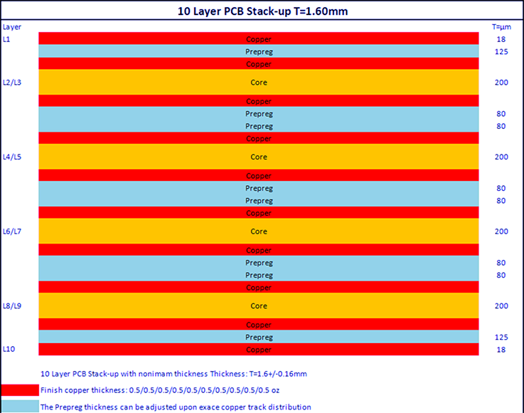
1. Top Layer (Signal Layer): This layer contains the topmost copper traces, which carry signals between components and connectors.
2. Signal Layer 2: This layer functions as an additional signal layer, providing space for more routing channels.
3. Ground Plane 1: This layer is dedicated to providing a solid ground reference plane, which helps to reduce noise and electromagnetic interference (EMI).
4. Power Plane 1: This layer serves as a power distribution plane, supplying power to components and ensuring proper power integrity.
5. Internal Signal Layer 1: This layer is located in the inner part of the PCB and is used for routing signals between components.
6. Internal Signal Layer 2: Similar to the previous internal signal layer, this layer provides additional routing channels for signals.
7. Ground Plane 2: Another ground plane is included in the stack-up to enhance shielding and reduce noise.
8. Power Plane 2: This layer acts as an additional power distribution plane to ensure sufficient power delivery.
9. Signal Layer 3: The third signal layer provides more space for routing signals.
10. Bottom Layer (Signal Layer): The bottom layer contains copper traces that handle signals and interconnections.
The specific arrangement and order of the layers in a 10-layer PCB stack-up may vary depending on the design requirements and considerations. The stack-up design must take into account factors such as impedance control, signal integrity, power distribution, and thermal management to achieve optimal performance and reliability.
Advantages of 10-Layer Stack-Ups
Utilizing a 10-layer PCB stack-up offers several advantageous features that contribute to the overall effectiveness and efficiency of the design:
1.Enhanced Design Flexibility:
The inclusion of additional layers in a 10-layer stack-up provides designers with greater flexibility to route complex circuitry and accommodate higher component density. This flexibility enables the implementation of intricate designs that may not be achievable with lower layer counts.
2.Improved Signal Integrity:
By incorporating dedicated power and ground planes within the stack-up, 10-layer PCBs effectively minimize noise, crosstalk, and electromagnetic interference (EMI). This results in improved signal integrity, reduced signal distortions, and reliable data transmission across the board.
3.Enhanced Power Distribution:
The presence of dedicated power planes within the 10-layer stack-up facilitates efficient power distribution throughout the PCB. These planes ensure effective power delivery, minimize voltage drops, and maintain a stable power supply across the board. This, in turn, reduces the risk of performance issues and ensures consistent operation of components.
4.Suitable for High-Density Designs:
The ample space provided by a 10-layer stack-up enables the accommodation of a larger number of components and more intricate routing patterns. This makes these stack-ups particularly well-suited for high-density designs where space optimization and intricate interconnections are crucial.
5.Cost-Effective:
Despite the increased functionality and design options offered by 10-layer stack-ups, they generally remain cost-effective compared to higher-layer configurations. This makes them an attractive choice for designs that require enhanced capabilities without significantly impacting the overall manufacturing cost.
Challenges of 10 layer PCB stack-up
While 10-layer PCB stack-ups offer numerous advantages, they also come with specific challenges that need to be addressed during the design and manufacturing process. These challenges include:
1.Increased Complexity:
As the number of layers increases, so does the complexity of the design. Managing the routing, vias, and interconnections between layers becomes more intricate and requires careful planning and consideration to avoid signal integrity issues and routing congestion.
2.Impedance Control:
Maintaining controlled impedance becomes more critical in 10-layer stack-ups due to the presence of multiple signal layers. Accurate impedance calculations and proper stack-up design are necessary to ensure signal integrity and prevent signal degradation or reflections.
3.Layer Alignment and Registration:
Aligning and registering all layers accurately during fabrication becomes more challenging with a higher layer count. Misalignment or registration errors can result in signal distortions, impedance variations, and difficulties in component placement.
4.Thermal Management:
With more layers comes an increased risk of heat buildup and inadequate thermal dissipation. Proper thermal management techniques, such as incorporating thermal vias, heatsinks, and copper pours, must be implemented to prevent overheating and ensure the reliability of the PCB.
5.Manufacturability and Yield:
The complexity of 10-layer stack-ups can pose challenges during the manufacturing process. Factors such as layer-to-layer registration, material compatibility, and proper lamination require careful attention to ensure high manufacturing yield and avoid costly reworks or scrap.
6.Cost:
While 10-layer stack-ups offer increased functionality, they generally come at a higher cost compared to lower layer counts. The additional layers, materials, and manufacturing complexities contribute to increased fabrication and assembly expenses.
7.Signal Integrity and EMI:
With more layers and complex routing patterns, the risk of signal integrity issues and electromagnetic interference (EMI) increases. Careful consideration of signal routing, proper ground and power plane design, and adherence to signal integrity guidelines are necessary to mitigate these challenges.
Addressing these challenges requires collaboration between PCB designers and manufacturers, careful stack-up planning, adherence to design guidelines, and advanced manufacturing techniques. By overcoming these hurdles, designers can fully harness the benefits of 10-layer PCB stack-ups while ensuring a reliable and high-performance end product.
How to Design a 10 Layer PCB Stack-up?
Designing a 10-layer PCB stack-up requires careful consideration of various factors to ensure optimal performance and reliability. Here are the key steps involved in designing a 10-layer PCB stack-up:
1. Determine Design Requirements: Understand the specific requirements of your PCB design, such as signal integrity, power distribution, thermal management, and impedance control. Consider the complexity of the circuitry, component density, and any specific design constraints.
2. Layer Allocation: Allocate the different layers based on their functions and requirements. Typically, the stack-up includes signal layers, power and ground planes, and internal signal layers. Decide on the number and arrangement of signal layers, power and ground planes, and any additional internal layers.
3. Signal Layer Placement: Determine the placement of signal layers based on the signal routing requirements and segregation of high-speed and low-speed signals. Position critical signal layers adjacent to power and ground planes for better signal integrity and noise reduction.
4. Power and Ground Planes: Allocate dedicated power and ground planes to ensure efficient power distribution and noise reduction. Determine the number and position of these planes to optimize power integrity and minimize voltage drops.
5. Impedance Control: Calculate and specify the required controlled impedance for high-speed signals. Ensure that the layer stack-up design and materials selected can achieve the desired impedance values. Consider factors such as trace width, dielectric thickness, and the choice of core and prepreg materials.
6. Layer Sequence and Ordering: Decide on the sequence and ordering of the layers in the stack-up. Consider factors such as signal integrity, heat dissipation, and ease of manufacturing. Typically, the stack-up starts with signal layers, followed by power and ground planes, and internal signal layers.
7. Material Selection: Choose suitable materials for the core and prepreg layers based on the design requirements. Consider factors such as dielectric constant, thermal conductivity, glass transition temperature, and compatibility with the manufacturing process.
8. Thermal Management: Incorporate thermal vias, copper pours, and additional copper layers to manage heat dissipation effectively. Position thermal vias strategically to connect heat-generating components to heat sinks or larger copper areas for efficient thermal transfer.
9. Design Rules and Constraints: Define design rules and constraints to ensure manufacturability and compatibility with the chosen PCB fabrication and assembly processes. Consider factors such as minimum trace width and spacing, minimum annular ring size, and minimum drill sizes.
10. Collaboration with Fabrication Partner: Work closely with your PCB fabrication partner to validate the stack-up design, ensure its feasibility, and address any manufacturing considerations or limitations that may arise.
It is crucial to consult industry standards, design guidelines, and experienced PCB engineers to optimize the 10-layer stack-up design for your specific application. Regularly review and iterate on the design to ensure it meets the desired performance, reliability, and manufacturability requirements.
How Do You Test the 10-layer PCB stackup?
When preparing to test the 10-layer PCB stack-up, several essential steps should be followed to ensure accurate and reliable results.
Firstly, it is crucial to verify the alignment of all layers within the stack-up. This can be accomplished by utilizing a precise layer alignment tool, which aids in ensuring the proper registration of each layer.
Next, the layers must be securely interconnected. This can be achieved through the use of adhesives or solder masks, which help establish solid connections and maintain the integrity of the stack-up structure.
Subsequently, the stack-up should undergo thorough testing to assess its performance. This involves subjecting the PCB to a controlled current. Accurate measurements can be obtained by utilizing specialized equipment such as multimeters or oscilloscopes, which enable the analysis of electrical characteristics and waveform behavior.
If the test results align with the desired specifications and meet the project requirements, it indicates the successful completion of the stack-up testing phase. At this point, one can proceed confidently to the subsequent stages of the project. However, in the event of any detected discrepancies or errors, it is imperative to address and rectify them promptly before progressing further. This diligent approach ensures the production of a high-quality PCB and mitigates potential issues that may arise during subsequent manufacturing and operation.
Consideration Factor When Selecting a 10-layer PCB Stackup
When selecting a 10-layer PCB stack-up, it is crucial to consider specific features that contribute to optimal performance. Paying close attention to these factors will help ensure the best results. Here are the key considerations when choosing a 10-layer PCB stack-up:
1. Layer Arrangement: It is essential to arrange signal layers adjacent to planes within the stack-up. This arrangement minimizes the number of signal layers embedded between different planes, which enhances signal integrity and reduces noise.
2. Tight Coupling: Ensuring tight coupling between signal layers and adjacent planes is critical. This entails maintaining a close proximity between the signal layers and their corresponding planes. It is recommended to keep the thickness of the signal layers below 10 MIL for optimal performance.
3. Signal Return Path: A well-designed 10-layer PCB stack-up should include a signal return path to improve overall performance. This can be achieved by incorporating a ground plane or power plane that serves as the signal return path.
4. Determining the Return Path: It is important to determine the specific plane that will serve as the return path for signals. For fast rise time signals, it is advisable to choose the path of least inductance, which typically involves routing the signal closest to the plane.
5. Cost Considerations: Budget allocation is an important factor to consider when selecting a 10-layer PCB stack-up. It is important to have a clear understanding that higher-quality stack-ups tend to come at a higher cost. Balancing performance requirements with budget constraints is crucial to make an informed decision.
By carefully considering these features, a well-designed 10-layer PCB stack-up can be selected that optimizes signal integrity, minimizes noise, and ensures reliable performance. Working closely with experienced PCB engineers and manufacturers can provide valuable insights and guidance throughout the selection process.
Comparison of 10-Layer and 12-Layer PCB Stackups
A 10-layer PCB stackup and a 12-layer PCB stackup differ in the number of layers they consist of. The layer count in a PCB stackup refers to the number of conductive layers (signal and power planes) present in the design.
In a 10-layer PCB stackup, there are typically 10 layers of conductive material, which includes signal layers for routing traces and power planes for distributing power and ground. The layer arrangement may vary based on the specific design requirements, but it commonly includes signal layers sandwiched between power and ground planes.
On the other hand, a 12-layer PCB stackup comprises 12 layers of conductive material. The additional layers can provide more flexibility in terms of routing and signal integrity. The extra layers can be utilized for adding more signal layers, power planes, or ground planes, depending on the design complexity and specific requirements.
The choice between a 10-layer and a 12-layer PCB stackup depends on the complexity of the circuit design, the need for signal integrity, power distribution, and other factors. More layers generally offer greater design flexibility and can help in achieving better signal performance, especially for high-speed or densely populated PCBs. However, adding more layers also increases the cost and complexity of the manufacturing process.
It’s important to note that the specific layer arrangement, materials used, and design considerations can vary based on the PCB manufacturer and the requirements of the specific application.
Popular Dielectric Material for 10-Layer PCB Stackup
The 10-layer PCB stackup commonly utilizes FR4 as the dielectric material in the manufacturing process. FR4 is available in the form of reimpregnated (prepreg) materials or as the core of the layer stackups. FR4 is chosen for its excellent fire retardant properties, making it resistant to easy combustion. Moreover, it exhibits favorable thermal properties, including a high glass transition temperature.
The high glass transition temperature of FR4, typically around 170 degrees Celsius, facilitates the manufacturing process of the 10-layer PCB stackup. A higher glass transition temperature ensures better stability and reliability during fabrication. By utilizing FR4 with a high Tg, the PCB manufacturer can achieve improved performance and durability of the 10-layer stackup.
In summary, the selection of FR4 as the dielectric material in the 10-layer PCB stackup is based on its fire retardancy, thermal properties, and high glass transition temperature. These characteristics contribute to the overall quality and reliability of the PCB during the manufacturing process.
Applications of a 10-Layer PCB Stack-up
10-layer PCBs find applications in a wide range of critical devices and systems, including those used in military and aerospace sectors. Here is a list of application areas where 10-layer PCBs are commonly utilized:
●Medical equipment
●Smartwatches and home appliances
●Computer and mobiles
●Industrial heavy machinery
●Telecommunication
●Satellites
●power amplifiers
●Automotive industry
●Military and defence
Summary
In this article, we have explored the stack-up design of a 10-layer printed circuit board (PCB) for advanced electronic applications. The stack-up design plays a crucial role in determining the performance and functionality of the PCB, especially in high-speed and high-frequency applications.
A well-designed stack-up ensures signal integrity, impedance control, and effective power distribution throughout the PCB. It involves carefully selecting the appropriate dielectric materials, copper weights, and layer arrangement to meet the specific requirements of the application.
Thefore, Adopting a 10-layer PCB stackup offers numerous advantages, including enhanced routing density, integrated shielding, precise impedance control, and efficient power distribution, all of which are crucial for cutting-edge electronic devices. However, achieving high-quality multilayer boards necessitates meticulous stackup planning and advanced manufacturing capabilities


