
Introduction:
The Evolution of Blind and Buried Vias in Modern PCB Design
If you’ve been following the latest trends in HDI PCB design, you’re probably aware that circuit boards today need to be smaller, faster, and more powerful. To achieve these goals, Blind Vias and Buried Vias are becoming must-have features for PCB engineers and designers.
These vias represent a shift from the traditional, large-hole methods used in older PCB designs. Their introduction has made it possible to increase circuit density without compromising performance or reliability. But what exactly are these vias, and how do they work?
In this article, we’ll delve deep into both Blind and Buried Vias, explaining what they are, their manufacturing processes, and the specific benefits they bring to high-density PCB designs. Whether you’re an HDI PCB designer, electronics manufacturer, or circuit board producer, gaining a solid understanding of these advanced vias can help you stay ahead in the industry.
The Rise of Blind and Buried Vias in HDI PCB Design
The world of HDI PCB design has evolved drastically in recent years, thanks in large part to Blind Vias and Buried Vias. These innovative via types have transformed how compact, high-performance circuit boards are crafted for modern electronics. Traditionally, circuit boards used through-hole vias, but the need for higher density, more complex circuits has led to the rise of these advanced via technologies. Blind Vias and Buried Vias allow us to optimize board space, improve signal integrity, and manage power more effectively, all while supporting smaller, faster, and more reliable devices.
Let’s dive deeper into the significance of Blind Vias and Buried Vias, looking at how they are pushing the boundaries of PCB design and enabling the development of cutting-edge electronics.
What Makes Blind and Buried Vias Important in Modern Circuit Boards?
Before we dive into the details of Blind and Buried Vias, let’s first understand what these vias actually are. A Blind Via is a hole that connects one or more outer layers of a PCB to an inner layer, but it doesn’t go all the way through the entire board. On the other hand, a Buried Via is a via that connects two or more inner layers of the PCB but doesn’t reach the outer layers.
So why does this matter? As electronics become more complex and smaller, the demand for miniaturized PCBs that can accommodate high-density components without sacrificing performance has increased. Blind and Buried Vias enable this level of miniaturization while providing more flexibility in the design process.
What makes these vias stand out is the ability to create more layered, complex circuits without adding too much extra space. This means that HDI PCBs can achieve higher-performance capabilities, this makes them indispensable for industries that require miniaturized electronics, such as smartphones, wearables, and automotive systems.
| Via Type | Description | Application |
| Blind Via | Connects outer layer to one or more inner layers. | Used in compact HDI PCBs, smartphones, and wearables. |
| Buried Via | Connects only the inner layers of the PCB. | Ideal for multi-layer boards, automotive systems, and medical devices. |
Evolution of Via Technology: From Simple Holes to Precision Vias
For years, PCB vias were simple, straightforward holes drilled all the way through the board, connecting the different layers of the PCB. As technology advanced and the demand for more compact and powerful electronic devices grew, therefore, we had to rethink the traditional via design. The shift from through-hole vias to Blind and Buried Vias allowed us to create boards with greater density, performance, and flexibility.
| Via Type | Technology Used | Impact on Design |
| Blind Via | Laser Drilling, Precision Drilling | Enables more compact, multi-layer designs without losing signal integrity. |
| Buried Via | Laser Drilling, Micro-Drilling | Ideal for inner layer connections, reducing complexity in outer layers. |
In recent years, via technology has progressed from using basic drilling techniques to adopting precision processes like laser drilling. These methods allow for tighter via placement, enabling us to maximize space on the board and accommodate more components. Today, the use of Blind and Buried Vias is standard in HDI and multilayer PCB designs because they meet the growing demand for more efficient and compact designs.
How the PCB Industry is Adapting to the Demand for Miniaturization?
With the consumer electronics market moving toward smaller devices that deliver higher performance, the PCB industry must keep up with these trends. Blind Vias and Buried Vias play an integral role in this push for miniaturization. By utilizing these vias, we can create HDI PCBs that meet the needs of high-end electronics, including smartphones, medical devices, and automotive systems.
Take wearable technology as an example—devices like smartwatches and fitness trackers demand compact yet highly capable PCBs. Blind and Buried Vias enable our designers to create smaller circuit boards that can juggle complex tasks such as signal processing, power management, and wireless connectivity. These advanced vias open the door to designs that pack a punch in performance without taking up much real estate, all while meeting the rigorous demands of modern devices.
| Device Type | Via Application | Why It Works |
| Smartphones | Blind Vias and Buried Vias connect internal components while freeing up space. | Enables high-density interconnect while maintaining slim profile. |
| Wearables | Buried Vias for inner layer connections. | Optimizes space for compact form factor and performance. |
| Automotive Systems | Blind Vias and Buried Vias improve signal integrity. | Ensures reliable communication in harsh environments. |
Understanding Blind Via & Buried Via
HDI PCBs (High-Density Interconnector PCBs) have become a cornerstone of modern electronics, enabling smaller devices that pack in more features without compromising efficiency. A major aspect of designing these advanced circuit boards involves working with Blind Vias and Buried Vias. These specialized pathways connect different PCB layers, optimizing signal transmission, freeing up surface space for components, and supporting compact layouts. This section unpacks the unique characteristics of these vias and sheds light on how they’re used in cutting-edge PCB production, offering a clear picture of their role in crafting today’s high-performance electronics.
What is a Blind Via?
A Blind Via is a hole drilled through a PCB that connects an outer layer to one or more inner layers. The key characteristic of a Blind Via is that it doesn’t penetrate the entire thickness of the PCB. Instead, it starts on the surface layer and extends only partway through the board, connecting to an inner layer below.
In HDI PCB manufacturing, Blind Vias are used to create a compact design by facilitating multi-layer interconnections without compromising the layout space on the outer layers. These vias are typically used when designing high-performance devices like smartphones, where the outer layers need to remain as free from interruptions as possible.
Examples of Blind Via Applications-
●Smartphone PCBs: Blind Vias enable PCB designers to connect multiple layers while keeping the outer surface clean for components like antennas and processors.
●Wearables: In devices like fitness trackers, Blind Vias allow for high-density circuits while maintaining a small, thin profile.
| Blind Via | Description | Application Example |
| Connection Method | Connects outer layer to inner layers | Smartphones, Wearables, Consumer Electronics |
| Drilling Depth | Does not go through the entire PCB | Used in compact designs to save space and improve functionality |
| Positioning | Located on the outer layers only | Maximizes space for external components and antennas |
Types of Blind Vias-
There are three types of blind vias for your information. We will examine each in depth here. The following diagram shows the various types of PCB vias.
Controlled Depth Drilled Vias
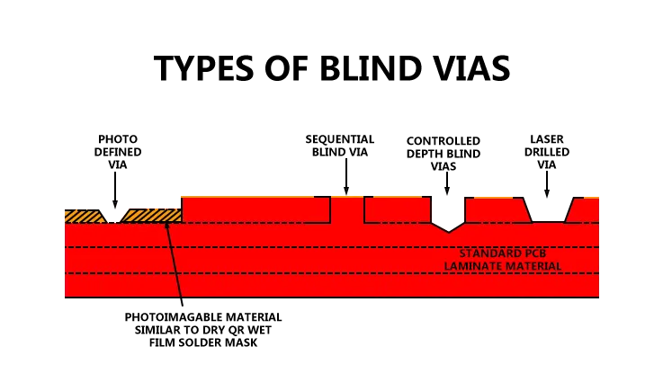
As shown , you can create controlled-depth vias by using the through-hole approach. But, it is important to use a drill that can pierce only halfway across the board. Additionally, a pad must be placed on the second layer in order to penetrate it with the drill. At the same time, it is helpful to be cautious to ensure that there are elements beneath the percolated hole and that they are in contact with the percolated hole. Moreover, you should apply the copper coating to the percolated holes in addition to plating copper inside the through-hole blind vias.
1.Photo-defined Blind Using PCB
A photo-reactive resin sheet can be coated onto a core to make a photo-defined blind. Cores should be composed of laminated traces ,and enriched with planes and submerged signal layers. It is recommended that you cover your photo-reactive sheet with patterns that shield the areas where you will make holes in it
Also, expose it to wavelength rays to make the residues harder in the circuit board. Then, you should immerse the circuit board into a mixture of dying to remove any undesirable substance from the holes.
Once you’ve finished the scraping process, you can plate copper in the holes as well as on the surfaces to create the surface layer on the board.
2.Sequential Lamination Blind Via
You can make this type of blind vias by passing a thin laminate piece through the two-faced PCB process. The first step is to drill, coat and draw the laminate in order to define the properties which will form the second layer of your PCB. Using the leave-the-solid copper material on the other PCB part as the first layer of your board. If you laminated the different layer of board your subassembly with the different board layers It would be best. The final step is to pass your product through the process of making multilayer surface layers.
3.Laser-drilled Blind Vias
These vias can be created after laminating all the board layers. You could create these vias prior to making the design and then covering your surface. Utilize a laser to eliminate the copper coating on the surface layer and also the insulating substance that is between the two layers. Be aware that you may make use of the Excimer laser or CO2 laser.
What is a Buried Via?
A Buried Via, unlike a Blind Via, is used solely to connect the internal layers of a PCB, never extending to the outer layers. These vias are a go-to solution for managing intricate internal layer connections in multilayer PCBs. They come into play where optimizing space and simplifying outer layer routing are top priorities. With their ability to reduce clutter and keep designs neat, Buried Vias are a practical choice for crafting high-density boards that deliver robust performance in compact, sophisticated devices.
Buried Vias offer a practical solution for designs that require smooth and uninterrupted outer layers. For example, in automotive electronics or medical devices, the focus is on internal connections that improve power distribution and signal integrity, without adding unnecessary components to the outer layers.
Example of Buried Via Applications-
●Automotive PCBs: In high-performance automotive electronics, Buried Vias are ideal for maintaining clean outer layers while ensuring robust internal connectivity.
●Medical Devices: Devices such as pacemakers and diagnostic equipment benefit from Buried Vias, which allow for complex internal connections without cluttering the outer layer.
| Buried Via | Description | Application Example |
| Connection Method | Connects only internal layers of the PCB | Automotive, Medical Devices |
| Drilling Depth | Does not connect to outer layers | Used in multi-layer designs for compact and efficient interconnections |
| Positioning | Internal connection, invisible from the outer layer | Maximizes efficiency in layered PCB designs |
Blind Via vs. Buried Via: Key Differences
While Blind Vias and Buried Vias may seem similar, they differ significantly in terms of design and manufacturing process. Here’s a breakdown of the key differences between the two:
| Aspect | Blind Via | Buried Via |
| Positioning | Connects an outer layer to inner layers | Only connects inner layers, no contact with outer layers |
| Manufacturing Process | Can be drilled using laser or mechanical methods | Requires precision drilling techniques to ensure accurate placement |
| Application | Used when external layer connections are required | Used for complex internal designs in multi-layer boards |
| Cost | Typically more cost-effective for smaller designs | Generally more expensive due to additional drilling and layer complexity |
Comparing Design Complexity-
●Blind Vias: Easier to implement in designs where you don’t need to disturb the external layers. Ideal for applications that don’t have stringent space limitations.
●Buried Vias: More complex, requiring more advanced drilling techniques and greater design precision. However, they provide superior performance in multi-layer designs, allowing the board to maintain a sleek outer layer.
Both Blind Vias and Buried Vias come with their own set of advantages and challenges, and the decision to use one over the other depends largely on the application’s design requirements and manufacturing capabilities. We need to weigh the cost, manufacturing complexity, and performance requirements when deciding on the right via type for their PCB design.
The Role of Blind and Buried Vias in High-Density PCB Design
When High-Density PCB design, Blind Vias and Buried Vias are key components that enable us to create efficient, compact, and high-performing circuit boards. These vias play a central role in helping us fit more functionality into smaller spaces, particularly as electronics shrink in size and demand more powerful capabilities. Let’s take a closer look at how Blind Vias and Buried Vias are integrated into the design process and what benefits they bring to modern circuit boards.
Maximizing Circuit Density with Blind Vias
Blind Vias are an effective way to increase circuit density by interconnecting various layers of the PCB without the need for full-through hole vias. In traditional PCB designs, through-hole vias connect the outer layers to inner layers, occupying significant space. However, Blind Vias allow for inter-layer connectivity while preserving valuable board real estate. These vias start on one outer layer and extend partially into the inner layers, helping to conserve space and increase the overall circuit density of the board.
In high-density designs, every bit of space is a big deal. Blind Vias make it possible to connect multiple layers without piling on extra thickness, helping pack more functionality into a smaller, sleeker design. This is a huge plus for devices like smartphones, tablets, and wearables, where compactness and performance go hand in hand. By using Blind Vias, we can fit all the necessary components in tighter spaces, ensuring the device doesn’t sacrifice power or usability.
Example Application-
Consider the evolution of smartphones. As device sizes have become more compact, many engineers have increasingly turned to Blind Vias to enable higher-density circuits without sacrificing performance. By using these vias, Some electronics manufacturers can design slimmer, more efficient phones while maintaining robust processing power, higher memory, and advanced capabilities.
| Blind Via Benefit | Effect on Design |
| Higher Circuit Density | Allows for more components to fit into a smaller board area |
| Space-Saving | Reduces the need for large through-hole vias, saving board real estate |
| Improved Component Layout | Maximizes space for external components like screens and antennas |
Increasing Design Flexibility with Buried Vias
Buried Vias offer another layer of flexibility in HDI PCB design, enabling us to connect inner layers of the PCB while leaving the outer layers free for components or external connections. These vias are especially useful when dealing with complex multilayer boards that require intricate internal routing.
By using Buried Vias, many PCB designers can route signals between different inner layers without disrupting the outer layers. This allows for greater design flexibility as it opens up new possibilities for optimizing space and improving routing efficiency, especially in multi-layer designs. For instance, engineers can manage heat distribution, power distribution, and signal integrity more effectively with the additional routing freedom Buried Vias provide.
Example Application-
In automotive electronics, for instance, Buried Vias are commonly used in multilayer PCBs for controlling power management and high-speed data transmission between multiple layers. These applications require precise routing to avoid interference while maintaining efficiency—Buried Vias allow for this without affecting the outer layers.
| Buried Via Benefit | Effect on Design |
| Enhanced Layer Connectivity | Enables complex signal routing between inner layers |
| Better Design Flexibility | Provides flexibility for high-density, multi-layer designs |
| Optimized Internal Routing | Helps with power, ground, and signal integrity in high-speed designs |
How Blind and Buried Vias Enable High-Density Interconnects?
High-Density Interconnects form the foundation of modern electronic devices, allowing for compact, efficient, and high-performing components. Blind Vias and Buried Vias make these advanced HDI designs possible by enabling us to create complex, densely packed circuits that maximize space. These vias help squeeze more capabilities into smaller boards, offering solutions for everything from sleek smartphones to cutting-edge wearables, all while keeping performance top-notch. With Blind and Buried Vias in play, it’s like fitting a full-size power engine into a compact car — lots of punch without the bulk.
Together, these vias allow for optimal use of space in high-performance devices. For instance, HDI PCBs are a common choice in industries like telecommunications, wearables, and automotive systems because they allow for high-speed signals and high-capacity power to travel between different layers without compromising the board’s size or structure. In HDI PCB design, Blind Vias and Buried Vias help to achieve smaller and more compact designs while maintaining signal integrity and reducing noise.
Example Application-
For smartphones, HDI PCBs with Blind and Buried Vias ensure that the circuit boards can hold the processor, memory, wireless antennas, and sensors in an efficient and compact way. Blind Vias allow components on the outer layer to stay uninterrupted, while Buried Vias maintain connections between inner layers to ensure smooth data transmission.
| HDI Via Benefit | Effect on High-Density Design |
| Optimized Layer Use | Reduces board thickness while maintaining connectivity |
| Improved Performance | Enables high-speed signals without taking up more space |
| Compact Design | Maximizes use of board space for complex, high-performance components |
Advanced Manufacturing Techniques for Blind and Buried Vias
In the world of HDI PCB manufacturing, achieving the precision and functionality necessary for compact, high-performance designs involves more than just selecting the right materials. Blind Vias and Buried Vias are made possible through cutting-edge manufacturing techniques that allow for exact placement and high-density interconnects. In this section, we’ll explore some of the advanced methods used to create these vias and ensure that they can handle the demands of modern electronics.
Laser Drilling for Blind Vias
When it comes to creating Blind Vias, laser drilling is the go-to method. This technique provides the precision drilling required to create vias that connect outer layers to inner layers of a HDI PCB without going all the way through the board. Laser drilling uses highly focused laser beams to melt or vaporize material, allowing for the creation of vias with extremely small diameters, tight spacing, and high accuracy. This technology has revolutionized the HDI PCB industry, providing PCB manufacturers with the ability to create intricate and densely packed circuit boards.
Why Laser Drilling Matters-
Laser drilling is a precise, non-mechanical process, which reduces the risk of damage to the PCB material. It allows our designers to place vias with minimal spacing between them, thereby maximizing circuit density. The ability to control the depth and diameter of the vias also reduces the likelihood of via failure due to improper hole dimensions, leading to enhanced reliability.
| Laser Drilling Benefit | Impact on HDI PCB Manufacturing |
| High Precision | Allows for accurate via placement with tight tolerances |
| Small Hole Sizes | Enables the use of Blind Vias with minimal space requirements |
| Reduced Mechanical Stress | Minimizes damage to the PCB during drilling, ensuring consistent quality |
Mechanical Drilling and Its Role in Buried Vias
While laser drilling is ideal for Blind Vias, mechanical drilling remains the go-to method for creating Buried Vias in multilayer HDI PCBs. In this process, a rotating drill bit is used to create holes in the PCB material. The depth of the hole can be precisely controlled to create vias that connect two or more inner layers while leaving the outer layers untouched.
Why Mechanical Drilling Works for Buried Vias-
Mechanical drilling is well-suited for creating Buried Vias because of its ability to precisely control via depth without penetrating the outer layers of the PCB. Since Buried Vias are placed between inner layers, they require an exact depth to ensure proper layer-to-layer connectivity. This method also allows for the use of larger diameter drill bits to create vias that can handle higher current and signal integrity requirements.
| Mechanical Drilling Benefit | Impact on Buried Via Creation |
| Controlled Depth | Ensures vias connect inner layers without penetrating outer layers |
| Flexibility in Via Size | Allows for larger via diameters for high-performance applications |
| Proven Process | Well-established technique that’s reliable in multilayer designs |
Plating and Filling Techniques for Via Reliability
Creating Blind and Buried Vias is only part of the equation in HDI PCB manufacturing. After the vias are drilled, they must undergo plating and filling processes to ensure their reliability and conductivity. Via plating involves depositing a layer of metal (usually copper) onto the walls of the drilled vias, while via filling involves filling the drilled hole with a conductive material to ensure proper electrical connectivity. Together, these processes help improve the overall via reliability, ensuring that the vias can handle the high-frequency signals and power requirements of modern electronics.
Why Plating and Filling Matter-
Plating and filling are integral to via reliability because they ensure the vias are conductive and can carry electrical signals between the various layers of the PCB without issue. Proper via plating creates a smooth, conductive surface that reduces the chance of signal loss or resistance. Via filling, on the other hand, prevents the formation of voids or weak points in the via, which can lead to board failures over time.
| Via Plating and Filling Benefit | Effect on Via Reliability |
| Improved Conductivity | Ensures efficient signal and power transmission through vias |
| Enhanced Mechanical Strength | Increases via durability, reducing the risk of failure over time |
| Prevention of Voids | Avoids weak spots that could cause electrical or mechanical failures |
Design Best Practices for Blind and Buried Vias in HDI PCB Layouts
When designing HDI PCBs, especially those incorporating Blind and Buried Vias, a thoughtful approach is necessary to create a layout that’s both compact and high-performance. These vias are a must-have for building multilayer boards with dense interconnections, but without careful planning, they can lead to design challenges. In this section, we’ll dive into some best practices that every PCB designer should keep in their back pocket when working with Blind and Buried Vias.
Optimizing Via Placement for Signal Integrity
Via placement is more than just determining where the holes go—it directly impacts the ability to preserve signal quality, particularly in high-speed designs. As circuit layouts become more complex, improper via positioning can lead to issues such as noise and signal interference. While Blind and Buried Vias offer advantages in compact designs, if not placed correctly, they can disrupt the smooth flow of signals. It’s a matter of ensuring the layout is optimized to prevent any issues that could affect the performance of the board, keeping it running as intended without interference.
Why Via Placement Matters-
When routing high-speed signals, the longer the path they take, the greater the chance of signal loss or interference. A poorly placed via can introduce impedance mismatches, leading to signal reflections that can degrade performance. On top of that, vias add capacitance and inductance, which can affect signal integrity.
So, how can you optimize via placement to keep things running smoothly?
●Best Practices for Via Placement:
1.Minimize Via Length: Always aim to reduce the distance between signal traces and vias. The closer a via is to a trace, the less time the signal will spend traveling through the via, reducing the potential for signal degradation.
2.Use Blind Vias Strategically: Since Blind Vias don’t go through the entire board, they are perfect for connecting outer layers to inner layers without interfering with signal paths on the other side of the PCB. When using Blind Vias, make sure they’re placed as close to the signal traces as possible to minimize signal loss.
3.Prioritize Critical Signals: For high-speed traces, avoid placing vias directly in the signal path. Instead, route the signals to areas of the PCB where vias can be strategically placed without disrupting the integrity of the signal. Signal layers should be clean and free of via interruptions to keep high-frequency signals crisp.
| Via Placement Strategy | Impact on Signal Integrity |
| Minimize Via Length | Reduces signal degradation and maintains speed |
| Strategic Placement of Blind Vias | Reduces interference by isolating signals on specific layers |
| Avoid Via in High-Speed Traces | Prevents signal reflections and impedance mismatches |
Managing Layer Stackup for Effective Via Integration
Properly designing the layer stackup is the foundation for integrating Blind and Buried Vias in multilayer PCB designs. Proper layer stackup allows for the effective integration of vias, enabling compact routing without sacrificing performance. It’s like a solid blueprint for your PCB—get it right, and everything fits like a glove; get it wrong, and you’ll be stuck with a tangled mess of connections.
Why Layer Stackup Matters-
The stackup determines how signals travel through the PCB layers and how easily vias can connect those layers. A poorly designed stackup might result in vias that are too deep, or placed incorrectly, leading to poor electrical performance or mechanical instability. A good stackup ensures that Blind Vias and Buried Vias are placed in the optimal position for electrical performance and ease of manufacturing.
●Best Practices for Layer Stackup:
1.Match Via Type with Layer Position: When designing a multilayer PCB, be mindful of where Blind and Buried Vias are located. Blind Vias are ideal for connecting outer layers to the first or second inner layers, while Buried Vias work better in deeper layers, making them suitable for complex internal routing.
2.Plan Layer Functions: Design your layers with specific functions in mind. High-speed signal layers should be separated from power or ground layers to minimize noise. Layer stackup can influence how easily vias are routed between different layers, so make sure that critical signals are routed in a way that minimizes via crossings.
3.Minimize the Number of Vias: A clean, simple stackup with as few vias as possible improves both manufacturability and performance. Use Buried Vias in areas where space is tight and the layers are already dedicated to non-critical signals.
| Stackup Management Strategy | Effect on Via Integration |
| Proper Layer Positioning | Ensures optimal via placement and reduces the chance of signal loss |
| Dedicated High-Speed Signal Layers | Keeps critical signals isolated and reduces interference from vias |
| Minimize Via Crossings | Reduces design complexity and improves signal integrity |
Balancing Via Density and Cost Efficiency
When designing HDI PCBs, balancing via density and cost efficiency is a tough but necessary task. Sure, we all want the highest performance possible, but too many vias—especially in Blind Vias and Buried Vias—can quickly increase the manufacturing cost. So, what’s the trick to keeping things efficient without sacrificing the quality of the design?
Why Balancing Via Density Matters-
In HDI designs, via density refers to how many vias are packed into a given area. Higher via density typically results in a smaller, more efficient PCB, but at the expense of cost. The more Blind and Buried Vias you use, the more expensive the board becomes to manufacture. Therefore, the challenge lies in finding a practical balance between achieving design goals and managing costs effectively.
●Best Practices for Balancing Via Density:
1.Use Vias Sparingly: Always ask yourself if a via is truly necessary. By optimizing the use of vias—especially Blind Vias and Buried Vias—you can maintain high-density interconnects without driving up costs.
2.Optimize Routing: If the via density is becoming too high, it may be time to rethink your routing strategy. Use layer stackup optimization to reduce the need for vias in non-critical areas.
3.Cost-Effective Materials: While via density is important, the choice of materials can also help manage costs. For instance, some HDI PCBs use laser drilling to create more vias with fewer steps, which can lower production costs.
| Density Balancing Strategy | Impact on Cost Efficiency |
| Minimize Via Count | Reduces cost by lowering material and processing expenses |
| Optimize Routing | Reduces via crossings and congestion, leading to a more cost-effective design |
| Use Cost-Effective Materials | Lowers material costs without compromising performance |
Challenges and Solutions in Blind and Buried Via Manufacturing
When diving into the manufacturing of Blind and Buried Vias, we will face various hurdles that can affect both performance and cost. The key to successful production lies in understanding and overcoming these challenges. Whether it’s the precision of via drilling, dealing with plating issues, or managing manufacturing yield, it all comes down to getting the details right. Let’s explore the common hurdles in via manufacturing and the solutions that help keep things on track.
Overcoming Drilling and Plating Challenges
One of the first hurdles in Blind Via and Buried Via manufacturing is the drilling process. It’s not just about punching holes in the board; it’s about ensuring precision while maintaining the integrity of each layer. As via drilling becomes more complex, manufacturers often face challenges that lead to plating defects and issues with via reliability.
Drilling Challenges-
●Precision: In HDI PCBs, the vias are smaller and more densely packed, requiring high precision during drilling. If the hole isn’t drilled correctly, it can lead to shorts or open circuits.
●Delamination: Incorrect drilling techniques can cause delamination, where the layers of the PCB separate. This results in via defects, which can compromise the electrical connection between the layers.
Plating Challenges-
●Uneven Plating: After drilling, the vias need to be plated to ensure proper conductivity. Uneven plating can result in weak or unreliable connections, which is particularly problematic in high-frequency designs.
●Void Formation: Voids in the plated via can lead to weak points in the PCB. These voids are often a result of poor control over the plating process, and they can undermine the overall performance of the PCB.
Solutions to Drilling and Plating Challenges-
1.Laser Drilling: For Blind Vias, laser drilling offers a high level of accuracy, ensuring that vias are drilled with minimal risk of delamination or improper hole sizes.
2.Advanced Plating Techniques: Electroless plating can improve the uniformity of the via plating process, reducing void formation and ensuring better overall via reliability.
3.Automated Inspection Systems: These systems can help detect plating issues or drilling inaccuracies early in the process, preventing defects from reaching the final product.
| Challenge | Solution | Impact on Quality |
| Precision in Drilling | Laser Drilling | Increased accuracy, reduced defects |
| Uneven Plating | Electroless Plating | More uniform plating, better conductivity |
| Voids in Plating | Automated Inspection | Early detection of defects, higher yield |
Reducing Defects and Improving Via Reliability
A significant challenge in Blind and Buried Via manufacturing is maintaining via reliability while minimizing defects. In high-density designs, defects can arise from several sources, including drilling inaccuracies, plating issues, and even improper via design. High-quality vias are a must for optimal performance in applications like smart devices or high-speed circuits. The goal here is to improve manufacturing yield by addressing these issues head-on.
Via Defects-
●Copper Pillar Separation: In some cases, copper plating may not adhere correctly, leading to separation or “lifting” of the copper pillars inside the via, which creates a defect.
●Via Blockage: Small Blind Vias can sometimes become blocked during drilling or plating, leading to incomplete electrical connections between the PCB layers.
Improving Via Reliability-
1.Process Control: Tight process controls at each step of the manufacturing process—drilling, plating, and inspection—can significantly reduce the risk of defects.
2.Via Design Optimization: The design phase should focus on optimizing via sizes and placement to avoid overcrowding and to ensure that each via is properly formed and plated. Avoiding overly small vias can help reduce the risk of defects.
3.Advanced Materials: Using high-quality copper or conductive materials can improve the adhesion of the plating, leading to more robust via reliability and fewer defects.
| Defect Type | Solution | Impact on Reliability |
| Copper Pillar Separation | Improved Adhesion Control | Stronger connection, higher reliability |
| Via Blockage | Optimized Via Design | Increased via yield, fewer electrical failures |
Managing Costs Without Compromising Quality
Navigating the challenges of HDI PCB manufacturing requires a sharp focus on cost management without compromising on quality. The use of Blind and Buried Vias can increase expenses due to the advanced techniques required for precise drilling and plating. However, with a smart approach that prioritizes efficiency and innovative solutions, it’s possible to strike the right balance between budget considerations and the demand for high-performance, dependable vias.
Cost Management Challenges-
●Complexity of Manufacturing: The advanced processes involved in making Blind and Buried Vias can drive up both material and labor costs. Additionally, maintaining quality control throughout the production process can add to the overall cost.
●Material Costs: High-quality via technology and the use of specialized materials, such as copper or conductive polymers, can increase the cost per unit.
Strategies for Cost Management-
1.Design for Manufacturability: Ensuring that the via design is as simple as possible while still achieving the necessary signal integrity can reduce the manufacturing complexity, which in turn reduces costs.
2.Volume Production: By increasing production volume, we can spread out the setup and labor costs, bringing the overall cost down. Large-scale production also allows for the use of more cost-effective materials.
3.Automation: Automating the drilling, plating, and inspection processes can reduce the labor cost per unit, streamline production, and lower the chances of defects.
| Cost Management Strategy | Impact on Manufacturing | Effect on Overall Quality |
| Design for Manufacturability | Reduces complexity and production cost | Maintains high signal integrity, reduces defects |
| Volume Production | Lower production cost per unit | Enables the use of better materials at a lower cost |
| Automation | Lowers labor costs and improves consistency | Higher quality, fewer defects |
Why Choose JarnisTech for Your Blind and Buried Via PCB Needs?
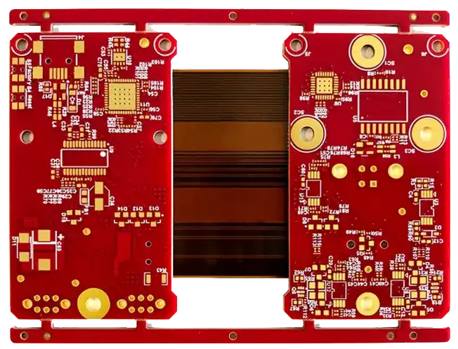
At JarnisTech, our state-of-the-art printed circuit board manufacturing facility is equipped with advanced machinery and cutting-edge processes, ensuring every board we produce meets the highest standards of quality and precision. Before production begins, each order undergoes a complimentary engineering file review by our experienced team. This process ensures your designs are optimized for functionality, helping you avoid costly errors and production delays. After all, no one wants to deal with PCBs that fail to perform—it’s a waste of time and resources.
We understand that timely delivery is just as important as quality. That’s why we specialize in quick-turn PCB production and offer expedited shipping options to meet even the tightest deadlines. Whether you’re working on a prototype or a large-scale production run, we make sure you receive your boards when you need them.
If your project involves advanced features like blind or buried vias, JarnisTech has you covered. We deliver top-tier PCBs that incorporate these technologies, ensuring optimal performance in high-density designs. Our skilled engineers and robust manufacturing processes guarantee reliability, whether your design includes blind vias, through holes, or a combination of both.
1.What Sets JarnisTech Apart?
●Comprehensive Engineering Support: Every design is thoroughly reviewed for manufacturability and performance, giving you peace of mind before production.
●Fast Turnaround: From design to delivery, our streamlined processes minimize lead times, getting your boards to you quickly.
●Top-Quality Manufacturing: We use premium materials and advanced techniques to produce PCBs that meet rigorous industry standards.
●Customer-Centric Approach: Our team is committed to delivering an exceptional experience, from initial consultation to post-delivery support.
For those seeking high-performance PCBs with advanced features like blind and buried vias, JarnisTech is your trusted partner. Let us help you turn your innovative ideas into high-quality products that stand out in the market.
2.Capabilities for Manufacturing
We utilize a mix of laser drilling controlled by depth as well as mechanical NC drilling to produce the blinds or vias that are buried. The manufacturing capabilities of conventional PCBs, as well as HDI PCBs, are as below:
| Via Type | Aspect Ratio | Ø Min | Ø Max | Via Pad | Annular Ring |
| Blind Via (mechanical) | 1:1 | 200μm | 300μm | 400μm | 100μm |
| Special Blind Fabrication | 1:1.2 | 150μm | 150μm | 350μm | 100μm |
| Blind Via (Laser) | 1:1 | 100μm | 100μm | 280μm | 90μm |
| Buried Via (mechanical) | 1:10 | 200μm | 400μm | 400μm | 100μm |
| Special Buried Fabrication | 1:12 | 150μm | 400μm | 330μm | 90μm |
HDI PCB uses a combination of buried and blind vias in addition to micro vias. With our state-of-the-art Laser Drilling Machine (Mitsubishi) and laser-direct imaging (LDI) which we have, we can provide quick delivery of HDI PCB prototyping.
3.Our HDI PCB Fabrication Capabilities
| HDI PCB Feature | Technical Specification |
| Layer Counts | 4 – 46 layers |
| HDI Builds | 1+N+1, 2+N+2, 3+N+3, 4+N+4…..7N7, Any layer in R&D |
| Materials | FR4, Halogen-free FR4, Rogers, and special raw laminate |
| Copper Weights (Finished) | 18μm – 70μm |
| Minimum Track and Gap | 0.075mm / 0.075mm |
| PCB Thickness | 0.40mm – 5.80mm |
| Maximum Dimensions | 610mm x 450mm |
| Surface Finishes Available | OSP, Immersion Gold (ENIG), Immersion Tin, Immersion Silver, Electrolytic Gold, Gold Fingers |
| Minimum Mechanical Drill | 0.15mm |
| Minimum Laser Drill | 0.1mm (Advanced) |
We’re thrilled to share everything we’ve learned about the blind and buried vias based on our experience of 20 years. We’re trusted with thousands of electronics engineers across the globe because of our 100% satisfaction guarantee policy. With our two-hour rapid response from our 24/7 tech and sales support team and our outstanding after-sales services, Please feel free to reach us at any time.
FAQs About Blind Vias & Buried Vias
How do blind and buried vias impact the thermal management of PCBs?
Blind and buried vias can influence heat dissipation by affecting the overall thermal conductivity of the board. Proper via design and integration of thermal vias can improve heat transfer in high-density applications.
Can blind and buried vias be used in flexible PCBs or rigid-flex designs?
Yes, blind and buried vias can be implemented in flexible and rigid-flex PCB designs, but their usage requires careful consideration of bending and stress points to avoid reliability issues.
What materials are best suited for PCBs with blind and buried vias?
High-performance materials like FR4, halogen-free FR4, and specialty laminates such as Rogers are commonly used. The choice depends on the board’s application, frequency requirements, and thermal management needs.
How does the aspect ratio affect blind and buried via reliability?
The aspect ratio (depth-to-diameter) significantly impacts the mechanical strength and plating uniformity of vias. Lower aspect ratios are easier to plate and result in more reliable connections, especially in multilayer designs.
Are blind and buried vias compatible with lead-free soldering processes?
Yes, blind and buried vias are compatible with lead-free soldering. However, the increased thermal stress of lead-free processes requires robust via design and high-quality materials to maintain performance.
What design rules should be followed for creating blind and buried vias in HDI PCBs?
Designers should adhere to manufacturer-specific guidelines, including minimum hole sizes, annular ring dimensions, and spacing requirements. Using design software with HDI capabilities can also streamline the process.


