Introduction:
The Art and Science of High Speed PCB Design
High speed printed circuit boards (PCBs) are at the heart of nearly every modern electronic device, from smartphones to high-performance computers and autonomous vehicles. Whether you’re constructing a next-gen 5G network or designing the latest consumer electronics, the integrity of your PCB’s signals is the make-or-break factor for ensuring top-tier performance and rock-solid reliability. . With the increasing demands for high-frequency signal transmission and advanced circuit designs, engineers and manufacturers must be up to speed with the latest design principles, materials, and manufacturing techniques to push the boundaries of what’s possible.
The Fundamentals of High-Speed PCB Design
When designing high-speed PCBs, it’s clear that the process goes far beyond merely connecting electronic components. The key challenge lies in ensuring that signals pass through the PCB with minimal loss, distortion, or interference. Think of it like a highway for data, but with no potholes or slow lanes. If signals get distorted, the entire system could go belly-up. From 5G to next-gen computing systems, ensuring signal integrity is a must.
So, for all the PCB design engineers out there, whether you’re just starting out or you’ve been around the block a few times, understanding the nitty-gritty of signal integrity, impedance control, and solid design practices is key to building reliable and fast circuits. Here’s the lowdown on what’s at stake and how to keep everything running smoothly.
Key Considerations for Signal Integrity in High-Speed PCB Design
When it comes to signal integrity, think of your signals as high-speed cars on a race track—everything’s gotta be clean and clear. If there’s interference or reflection, it’s like a bump in the road, messing up the whole ride.
Signal Reflections-
One of the most critical issues when designing high-speed circuits is signal reflection. This occurs when there’s an impedance mismatch between the trace and the load at the end of the transmission line. If the impedance of the PCB trace doesn’t match the impedance of the load, the signal is reflected back, leading to distortion. For instance, in digital communications, this could lead to bit errors, corrupting data transmission.
| Impedance Mismatch (%) | Reflection Coefficient (%) |
| 0% (perfect match) | 0% |
| 5% mismatch | 2.5% |
| 10% mismatch | 5.0% |
| 20% mismatch | 10% |
A mismatch of just 10% can result in noticeable signal distortion, potentially leading to errors. To mitigate this, designers incorporate termination resistors at the end of the trace to absorb reflections, and they use controlled impedance to ensure the trace impedance matches the load impedance.
Signal Attenuation-
Another challenge when designing high-speed circuits is signal attenuation, which occurs when the signal weakens as it travels along the PCB traces. The longer the trace, the more signal is lost. This becomes even more problematic at higher frequencies, where attenuation is more pronounced. Choosing low-loss PCB materials like Rogers or Teflon can help reduce the effects of attenuation, ensuring that signals maintain their integrity over longer distances.
| Material Type | Signal Loss at 10 GHz (dB/inch) | Recommended Use |
| FR4 | 1.5 | General use, standard designs |
| Rogers 4003C | 0.2 | High-frequency, low-loss designs |
| Teflon | 0.1 | High-speed, low-loss applications |
So, to keep your signals from dropping like a bad signal at a concert, you need to pick the right materials—something that’ll keep them alive and kicking as they make their way down the trace.
Impedance Control and Its Importance in High-Speed PCB Design
Impedance control is the practice of ensuring that the impedance of the PCB traces is consistent and matches the impedance of the components they connect to. Without impedance control, it’s like having a system where all lanes are closed except one—your signals will just get stuck, and that’s a major bottleneck. In high-speed PCB design, controlling the impedance of the traces ensures your signals flow without losing any juice. When your impedance is mismatched, it’s like a car going too fast for a curve—it’ll lose control.
Differential Pairs-
One commonly used technique in high-speed PCB design is differential pairs, which consist of two traces carrying equal and opposite signals. By routing the traces closely together and maintaining the same length, differential pairs help to cancel out common-mode noise and prevent signal degradation.
For example, in designs for high-speed USB 3.0 circuits, differential pairs are routed with a controlled impedance of 100Ω, ensuring that the signal remains clean and interference-free.
| Differential Pair Impedance (Ω) | Trace Spacing (mil) | Trace Width (mil) |
| 100Ω | 6 mil | 4 mil |
| 90Ω | 5 mil | 3 mil |
| 110Ω | 8 mil | 5 mil |
Trace Length, Routing, and Their Effect on Signal Performance
In high-speed PCB design, trace length directly affects signal delay. Longer traces result in higher delays, which can cause timing issues within the circuit. Proper routing of the traces helps minimize these delays and preserves signal integrity.
Effect of Trace Length on Signal Delay-
As trace lengths increase, so does the propagation delay. This delay is especially pronounced in high-frequency designs. If the trace is too long, it may cause timing mismatches, leading to data errors or malfunctioning circuits.
| Trace Length (inches) | Propagation Delay (ns) | Signal Delay (ns) | Effect on Signal Performance |
| 1 inch | 1.5 ns | 1.5 ns | Minimal delay in most designs. |
| 5 inches | 7.5 ns | 7.5 ns | Noticeable delay, timing issues in some designs. |
| 10 inches | 15 ns | 15 ns | Significant delay, possible misalignment in signals. |
| 20 inches | 30 ns | 30 ns | Major delay, leads to timing issues and synchronization errors. |
Routing Techniques to Minimize Signal Delay-
To minimize signal delay, high-speed PCB designers typically apply several strategies:
●Minimize via usage: Vias add inductance and cause signal degradation, so they are used sparingly.
●Avoid sharp corners: Sharp angles in trace routing lead to impedance mismatches and signal reflections. Using curved traces helps to maintain signal quality.
●Use multiple layers: In multi-layer PCBs, high-speed signals are routed on the optimal layers to reduce the trace length and avoid unnecessary routing paths.
Impact of Via Types on Signal Integrity-
The type of via used in the PCB design can significantly affect signal integrity. There are several types of vias, each with its impact on high-speed signal performance:
| Via Type | Signal Impact | Recommended Use |
| Through-Hole Via | Adds signal degradation due to higher inductance. | Best avoided in high-speed designs unless necessary. |
| Blind Via | Provides shorter paths with less signal degradation. | Ideal for multi-layer designs where high-speed signal integrity is critical. |
| Buried Via | Minimal signal impact, routed entirely within the PCB layers. | Optimal for high-density, high-speed designs where minimizing signal loss is paramount. |
Using blind vias or buried vias might cost more, but they’ll keep your signals running clean, like a well-oiled machine.
Advanced Materials for High-Speed PCB Design
When designing high-speed PCBs, selecting the appropriate materials requires careful attention to detail. It’s not just about choosing commonly used options, but rather identifying materials that optimize signal integrity, minimize signal loss, and provide effective heat dissipation. In this section we will explore high-speed PCB materials, including brands like Rogers, Shengyi, Panasonic, Isola, and others, offering a comprehensive overview of each one and how it impacts the design and performance of your PCB.
Selecting the Right Materials for High-Speed PCB Applications
Selecting the right substrate material for high-speed PCBs involves more than just knowing the dielectric constant and thermal conductivity. It also requires considering the signal degradation, material cost, fabrication ease, and specific frequency requirements. Here, we will look at various high-speed PCB materials and how to choose the best one based on your design needs.
Common High-Speed PCB Materials-
●Rogers PCB – Known for their low signal loss and high-frequency capabilities, Rogers materials like RO4003C and RO4350B are frequently used in high-frequency applications such as microwave communication, 5G, and RF circuits. These materials offer consistent dielectric constants and low loss tangents, making them ideal for high-speed digital and analog signal transmission.
●Shengyi PCB – A leading manufacturer of high-frequency PCB materials, Shengyi offers a range of materials including S1000-2 and S1166 that are used in high-speed data transmission. Their materials provide superior thermal performance and excellent dielectric properties, ensuring signal fidelity even at high speeds.
●Panasonic PCB – Panasonic’s Megtron series is specifically designed for high-frequency applications. With materials like Megtron 6, which boasts low loss and high thermal conductivity, these materials are perfect for applications that demand high-speed signal integrity and thermal dissipation.
●Isola PCB – Isola’s IS680 and IS420 offer low-loss characteristics and are designed for high-speed digital and RF circuits. These materials are ideal for 5G and communications infrastructure, providing excellent dielectric stability and signal preservation over a wide frequency range.
●Teflon PCB – Teflon materials are used in ultra-high-speed microwave and RF circuits. Teflon (PTFE) has a low dielectric constant and loss tangent, making it ideal for high-frequency signal integrity applications that require minimal signal attenuation.
●Arlon PCB – Materials like ARLON 25N are designed for high-performance applications with excellent thermal stability and signal propagation characteristics. These are often used in telecommunications, automotive electronics, and military systems.
●Ventec PCB – Known for their high-performance laminates such as VT-901 and VT-825, Ventec offers materials with good thermal conductivity and low signal loss, perfect for high-frequency communications and automotive electronics.
●Dupont PCB – Dupont’s TEFLON and FR-4 variants are well known for their high thermal resistance, low loss, and good mechanical properties, making them suitable for a variety of high-speed PCB applications.
●BT PCB – BT resin is a popular choice for high-speed PCB applications because of its low dielectric constant and excellent thermal dissipation capabilities, often found in computing, automotive, and communications electronics.
| Material Type | Dielectric Constant (Dk) | Loss Tangent (Df) | Thermal Conductivity (W/m·K) | Applications |
| Rogers 4003C | 3.38 | 0.0025 | 0.25 | RF, Microwave, 5G, High-speed digital |
| Shengyi S1000-2 | 4.0 | 0.01 | 0.35 | High-speed data, Telecommunications |
| Panasonic Megtron 6 | 3.3 | 0.003 | 0.50 | High-frequency, Microwave, Automotive |
| Isola IS680 | 3.25 | 0.004 | 0.45 | 5G, High-speed communications, RF |
| Teflon (PTFE) | 2.1 | 0.0002 | 0.22 | Ultra-high-speed, RF, Microwave |
| Arlon ARLON 25N | 3.2 | 0.005 | 0.30 | Automotive electronics, Military, RF |
| Ventec VT-901 | 3.5 | 0.003 | 0.40 | Telecommunications, High-speed computing |
| Dupont TEFLON | 2.1 | 0.0001 | 0.18 | High-speed, Low-loss, RF, Microwave |
| BT Resin | 3.0 | 0.0035 | 0.40 | High-speed computing, Automotive, RF |
These materials provide the low-loss characteristics, dielectric stability, and thermal conductivity required for high-speed PCB applications. Choosing the right material from these brands can significantly improve the performance of your high-speed PCB.
The Role of Loss Tangent and Dielectric Constant in Signal Integrity
When designing high-speed PCBs, signal integrity isn’t something you can take lightly. The materials you choose directly impact how well your signals travel through the board. Two factors that come into play here are the loss tangent and dielectric constant.
Loss Tangent and Signal Degradation-
The loss tangent of a PCB material tells you how much signal is lost as it travels through the substrate. A low loss tangent means less signal degradation, and a high loss tangent means more energy is dissipated, leading to weaker signals. In high-speed designs, you want materials with the lowest loss tangent possible to minimize signal degradation.
| Material Type | Loss Tangent (Df) | Signal Loss at 10 GHz (dB/inch) | Use Case |
| Rogers 4003C | 0.0025 | 0.2 | High-frequency, RF |
| Shengyi S1000-2 | 0.01 | 1.5 | General data transmission |
| Panasonic Megtron 6 | 0.003 | 0.1 | Microwave, Automotive |
| Isola IS680 | 0.004 | 0.5 | 5G, RF communications |
| Teflon (PTFE) | 0.0002 | 0.1 | Low-loss, RF, High-speed |
As you can see, Teflon materials offer the lowest loss tangent, making them ideal for high-speed signals and microwave frequencies. On the other hand, Shengyi S1000-2 and Isola IS680 provide better cost-effective options for medium to high-speed applications without sacrificing too much in terms of performance.
Dielectric Constant and Signal Propagation-
The dielectric constant (Dk) of a material impacts how quickly signals move through it. A higher Dk causes slower signal transmission. In high-speed PCB designs, achieving the right Dk balance helps keep signals aligned. The lower the Dk, the faster the signal travels.
Comparing Traditional and High-Speed PCB Materials
Let’s compare traditional materials like FR4 to high-speed PCB materials such as Rogers, Shengyi,Teflon and etc). As the design complexity increases, you’ll find that FR4 simply doesn’t cut it for high-speed applications. So, let’s break down the main contenders:
| Material Type | Dielectric Constant (Dk) | Loss Tangent (Df) | Thermal Conductivity (W/m·K) | Best Use |
| FR4 | 4.2 | 0.02 | 0.3 | Basic circuits, low-frequency |
| Rogers 4003C | 3.38 | 0.0025 | 0.85 | High-speed, RF, 5G |
| Teflon (PTFE) | 2.1 | 0.0002 | 0.7 | Ultra-high-speed, microwave |
| Shengyi S1000-2 | 4.0 | 0.01 | 0.4 | Digital signals, telecom |
| Isola I-Tera | 3.2 | 0.004 | 0.6 | High-speed, RF circuits |
| Arlon 25N | 3.0 | 0.004 | 1.0 | Microwave, high-frequency |
Bottom line: if you’re looking to push your designs to the max with high-speed signals, ditch the old standbys and go for advanced PCB materials like Rogers or Arlon. They’re not just “better,” they’re designed specifically to handle high-frequency and low-loss applications with precision.
Advanced Stackup Design for High-Speed PCBs
When you’re designing high-speed PCBs, the stackup design isn’t just a technical choice—it’s the backbone of your entire project. Think of it like building a skyscraper. If the foundation isn’t solid, everything above it is at risk of crumbling. That’s why getting your multilayer PCB stackup right is non-negotiable. A well-thought-out stackup ensures your signal integrity stays top-notch, while also optimizing for performance across all layers.
Designing an Optimal Stackup for Signal Integrity and Performance
When it comes to designing an optimal stackup, it’s like crafting a perfect sandwich: you need the right layers in the right order to keep everything from falling apart. A poor stackup can create all kinds of issues, from signal interference to performance degradation. Here’s what you need to keep in mind:
1.Multilayer Stackup: A multilayer stackup in high-speed PCB design provides flexibility in routing high-speed signals, managing ground planes, and controlling impedance. By carefully selecting the sequence and thickness of each layer, designers can minimize signal loss and ensure that high-speed signals move from point A to point B without unnecessary delays or interference.
2.Signal Path Optimization: Think of this as designing a highway with as few detours as possible. The fewer the obstacles, the faster your signals can travel. For high-speed designs, this means making sure that high-speed signal traces are as short as possible and that they’re routed over a solid ground plane. Avoiding unnecessary via transitions and long trace runs will help keep the signal’s speed and quality intact.
3.Stackup Considerations: For each high-speed PCB design, factors like trace width, layer thickness, and material type must be carefully considered. Take, for example, Rogers 4003C: it offers great dielectric properties and low loss at high frequencies, making it an ideal choice for optimizing signal integrity in a multilayer stackup.
Here’s a snapshot of a typical high-speed PCB stackup:
| Layer | Purpose | Material | Thickness | Signal Speed |
| Top Layer | High-speed signal routing | Rogers 4003C | 0.2 mm | Fast |
| Ground Plane | Signal reference, shielding | Copper | 0.35 mm | N/A |
| Inner Layer 1 | Power distribution | FR4 | 0.2 mm | Moderate |
| Inner Layer 2 | Signal routing | Rogers 4003C | 0.2 mm | Fast |
| Bottom Layer | High-speed signal routing | Rogers 4003C | 0.2 mm | Fast |
Impedance Matching and Layer-to-Layer Alignment in High-Speed PCBs
Impedance matching in high-speed PCBs is like tuning an instrument: if it’s off, the sound (or in this case, the signal) won’t be as sharp and clear as it should be. To avoid reflections and ensure smooth signal transmission, every layer of the stackup needs to be carefully aligned. This includes ensuring impedance matching between signal layers, power planes, and ground planes.
1.Impedance Matching: In high-speed PCB design, impedance mismatch is one of the biggest culprits behind signal distortion. By aligning the impedance of your traces with that of the source and load, you ensure that signals flow without causing reflections or loss. If you’re working with differential pairs, for example, the traces should be routed close together and with precise spacing to maintain controlled impedance.
2.Layer-to-Layer Alignment: Think of layer alignment as keeping all the gears in a machine well-oiled and meshed. In multilayer stackups, misaligned layers can cause signal degradation and introduce crosstalk. Proper alignment between layers helps to maintain the integrity of the signal path, ensuring that high-speed signals move smoothly from layer to layer without unwanted interference.
Here’s a basic example of impedance matching in a high-speed PCB stackup:
| Layer | Signal Type | Impedance | Material | Alignment Consideration |
| Top Layer | High-speed signal | 50 Ohms | Rogers 4003C | Aligned with ground plane |
| Inner Layer 1 | Power distribution | N/A | FR4 | Ground planes should be aligned |
| Inner Layer 2 | Signal routing | 50 Ohms | Rogers 4003C | Maintain impedance match |
| Bottom Layer | High-speed signal | 50 Ohms | Rogers 4003C | Controlled impedance routing |
Minimizing Crosstalk and Signal Loss in High-Speed Stackups
Now, let’s talk about the dreaded crosstalk and signal loss. If you want your high-speed PCB design to work like a well-oiled machine, you’ve got to keep these two bad boys in check. Crosstalk happens when signals from adjacent traces interfere with each other, while signal loss occurs when part of the signal energy dissipates due to resistance, inductance, or other factors. Here’s how to minimize both:
1.Crosstalk Reduction: To reduce crosstalk, designers often increase the spacing between signal traces or use ground planes to shield them. Another effective strategy is to keep high-frequency signals away from low-frequency signals, as these are more prone to causing interference. For example, routing sensitive clock signals separately from other high-speed signals can significantly reduce the potential for crosstalk.
2.Signal Loss Minimization: Signal loss is a natural part of signal transmission, but it doesn’t have to be a dealbreaker. By carefully selecting materials with a low loss tangent, such as Rogers RO4003C or Teflon, designers can significantly reduce signal degradation. Additionally, optimizing trace width and thickness can help reduce the overall resistance and inductance of the traces, which in turn minimizes signal loss.
Check out the following table for a quick look at how different stackup configurations affect crosstalk and signal loss:
| Stackup Configuration | Signal Loss (dB) | Crosstalk (dB) | Recommended for |
| Basic FR4 Stackup | High | Moderate | Low-frequency designs |
| Rogers 4003C Stackup | Low | Low | High-frequency, 5G, RF designs |
| Teflon Stackup | Ultra-Low | Ultra-Low | Ultra-high-speed, microwave |
High-Speed PCB Routing and Layout Best Practices
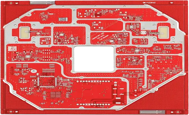
Designing a high-speed PCB isn’t just about throwing down components and connecting them. It’s like building a precision machine—every trace, every via, and every layer must be meticulously planned. If you want your high-speed signals to make it from point A to point B without hitting traffic, PCB routing is the way to go. Whether you’re routing high-frequency signals, managing differential pairs, or optimizing vias, each step requires careful attention to ensure signal integrity stays intact. Here’s how to nail your PCB routing and layout, and why the details matter.
Best Practices for Routing High-Speed Signals
Routing high-speed signals isn’t as straightforward as dealing with low-frequency ones. These signals travel at incredible speeds, and with that speed comes potential issues like distortion and loss. Poor routing can leave you with signals full of noise instead of clear data. Here’s how to properly handle high-speed signal routing to avoid these pitfalls.
●Trace Optimization: The trace width, trace spacing, and trace length can directly affect the performance of high-speed signals. A longer trace means more resistance, inductance, and potential signal degradation. The best practice is to keep trace lengths as short as possible while ensuring enough space between traces to avoid crosstalk. This is especially true for signals running in the gigahertz range.
For instance, if you’re routing a high-speed clock signal, you should keep the trace as short as possible and avoid sharp bends that could introduce signal reflection. Traces should be routed on the inner layers of the PCB and preferably close to a ground plane to ensure proper signal reference and reduce the chance of interference.
●High-Speed Routing Guidelines: One of the golden rules of high-speed routing is to minimize the number of vias. Each via adds capacitance and inductance, which can slow down or degrade the signal. Try to keep routing through vias to a minimum and use via-in-pad or blind vias when necessary to keep signals as direct as possible. Another tip is to avoid running high-speed signals parallel to one another for long distances—this helps to reduce the risk of crosstalk and noise.
Here’s a quick look at some routing best practices for high-speed signals:
| Routing Practice | Description | Why It Matters |
| Minimize Trace Lengths | Keep signal traces as short as possible | Reduces signal degradation and delay |
| Use Ground Planes | Route signals over solid ground planes | Ensures signal integrity and reduces noise |
| Avoid Sharp Bends | Avoid 90-degree bends in signal traces | Prevents signal reflections and degradation |
| Limit Via Use | Minimize the use of vias, use blind vias if needed | Reduces impedance mismatch and signal loss |
| Keep Signals Separate | Separate high-speed signals from low-speed ones | Reduces crosstalk and prevents noise interference |
Managing Differential Pairs and Impedance Control in High-Speed Layout
When it comes to high-speed layouts, differential pairs and impedance control go hand in hand. Imagine them as dance partners: if one is out of sync, the whole performance falls apart. Getting these two elements right ensures that your high-speed signals travel smoothly and without degradation.
●Differential Pairs: Differential pairs are key when working with high-speed signals, especially in systems like Ethernet or USB. For proper signal transmission, the two traces in a differential pair need to be routed as close together as possible and maintain a consistent distance (pitch). The impedance between the pair should also be tightly controlled to prevent signal reflections.
A typical differential pair routing involves maintaining controlled impedance (usually around 100 ohms for many high-speed designs). Keeping the distance between the two traces uniform and ensuring the pair is as close to a reference plane as possible minimizes signal degradation and maximizes signal integrity.
●Impedance Control: Impedance control is all about ensuring that the signal impedance matches the impedance of the source and the load. When impedance mismatches occur, part of the signal reflects back toward the source, leading to potential data corruption or signal loss. To ensure impedance matching, therefore, to maintain uniform trace width, spacing, and layer stackup across your PCB.
Here’s an example of differential pair routing:
| Parameter | Value | Description |
| Trace Width | 4 mils | Width of each trace in a differential pair |
| Trace Spacing | 6 mils | Distance between the two traces in a differential pair |
| Impedance | 100 ohms | Target impedance between the two traces |
| Layer | Inner Layer | Layer where the differential pair is routed |
Via Design for High-Speed PCB Applications
Let’s talk about vias—those little connectors between layers. At first glance, vias might seem like a minor detail, but in high-speed PCB design, they’re anything but. Poorly designed vias can introduce a significant amount of signal loss and degrade performance, especially at high frequencies. But with the right via design, you can avoid these issues and improve overall signal quality.
●Via Optimization: Via optimization is all about reducing the negative impact that vias have on your signal. When designing vias, you want to minimize via stub length and choose blind vias or buried vias whenever possible, as they tend to offer lower inductance and resistance compared to through-hole vias. Also, choosing vias with lower capacitance and inductance values also helps keep your signals crisp and reliable
●Via Stub Reduction: A via stub is the part of the via that isn’t used to connect layers but still adds resistance and inductance to the signal path. The longer the stub, the more it interferes with signal transmission. Via stub reduction involves shortening the stub or using a via with a direct path between layers. This reduces the potential for signal loss and improves the overall quality of the signal.
Here’s a look at how via design can impact signal quality:
| Via Type | Inductance | Capacitance | Signal Impact |
| Through-hole Via | High | High | Increased signal loss and impedance mismatch |
| Blind Via | Low | Low | Minimizes signal loss, better impedance control |
| Buried Via | Low | Low | Best for high-speed designs, least signal degradation |
High-Speed PCB Manufacturing: From Design to Production
When it comes to high-speed PCB manufacturing, there’s no room for second chances. Designing a high-speed PCB is one thing, but turning that design into a real, functioning board that meets performance standards is a whole other ballgame. The fabrication process has to be sharp—no tolerance for sloppiness, no room for error. It’s all about precision manufacturing and ensuring that every step, from initial design to final production, is executed with impeccable accuracy.
Best Practices in High-Speed PCB Manufacturing
The PCB is manufacturing process can heavily influence how well your high-speed design performs in real-world applications. Even if the design checks all the right boxes, the production process needs to meet the same level of precision to avoid introducing issues like signal loss or crosstalk. From material prep to final assembly, every step matters when it comes to translating your design into a top-notch product.
1.Precision in PCB Production: To ensure optimal signal integrity, every aspect of the PCB fabrication process must adhere to tight tolerances. The width of each trace, the spacing between traces, and the layer alignment must be maintained to exact specifications. Even the slightest deviation can introduce unwanted resistance, inductance, or signal degradation. Think of it as precision engineering—every detail matters.
2.High-Speed PCB Production: Unlike standard PCBs, high-speed PCBs demand more from the manufacturing process. The process needs to account for the higher frequencies that these boards carry. Everything, from the choice of material to the application of copper plating, plays a part in ensuring that the PCB performs at peak levels. Whether it’s using advanced PCB fabrication techniques or managing specific thermal requirements, each decision has a ripple effect on the performance of your high-speed circuits.
High-speed PCB production best practices-
| Production Step | Best Practice | Why It Matters |
| Material Selection | Use low-loss, high-frequency PCB materials | Ensures minimal signal degradation at high speeds |
| Copper Plating | Use high-quality copper plating with minimal oxidation | Reduces signal resistance and maintains integrity |
| Layer Alignment | Keep layer-to-layer alignment tight | Prevents impedance mismatch and signal reflections |
| Surface Finish | Use high-frequency finishes (e.g., ENIG, HASL) | Improves signal quality by reducing surface roughness |
Managing Tolerances and Minimizing Signal Degradation in Manufacturing
Let’s be real: Fabrication tolerances are the unsung rules that can make or break your high-speed PCB, much like the hidden clauses in a deal you wish you’d read. When it comes to high-frequency designs, even the tiniest deviations in trace width, via dimensions, or spacing can wreak havoc on signal quality and derail the board’s performance. Ignoring these details isn’t just rolling the dice—it’s setting yourself up for potential headaches down the line. Let’s dig into the strategies that ensure your manufacturing process stays on point and doesn’t leave you footing the bill for avoidable errors.
1.Fabrication Tolerances: High-speed PCBs require tight tolerances, usually in the range of ±0.05mm for trace width and spacing, and even tighter tolerances for via placement. Signal integrity can quickly degrade if these tolerances aren’t maintained. For instance, if the distance between two high-speed signal traces isn’t kept at the right distance, crosstalk can occur, leading to interference between the signals.
2.Manufacturing Precision: Beyond trace widths, the accuracy of via drilling, plating thickness, and stackup alignment also plays a role. Even the thermal management of the PCB during manufacturing can affect signal transmission. Poor heat dissipation can cause traces to expand and contract, further affecting signal integrity.
Here’s an example showing the impact of manufacturing tolerances:
| Parameter | Tolerance | Impact of Deviation |
| Trace Width | ±0.05mm | Deviation can result in impedance mismatch and signal reflection |
| Via Size | ±0.1mm | Larger vias cause higher inductance and impedance issues |
| Layer-to-Layer Alignment | ±0.05mm | Misalignment leads to poor signal integrity and crosstalk |
Advanced Fabrication Techniques for High-Speed PCBs
The world of high-speed PCB fabrication is constantly evolving, and with it come advanced manufacturing techniques that push the boundaries of performance. These cutting-edge methods are designed to address the unique challenges of high-frequency signal transmission, reducing signal loss, and improving overall performance.
1.Copper Plating for High-Speed PCBs: In high-speed PCB manufacturing, copper plating quality can make all the difference in how the board performs at higher frequencies. . High-quality copper ensures lower resistance and signal integrity at higher frequencies. The process involves depositing a thin, uniform layer of copper over the PCB, which is then etched to form the traces. Any defects or uneven plating can lead to impedance mismatches and poor signal transmission.
2.High-Frequency Finishes: The surface finish of the PCB can significantly impact its performance, especially for high-speed circuits. Electroless Nickel Immersion Gold (ENIG) and HASL are some of the most common finishes used for high-speed PCBs, as they provide excellent electrical performance and resistance to oxidation. These finishes reduce signal loss and reflection, which are often issues with other PCB finishes.
3.Advanced Materials and Processes: Advanced PCB fabrication techniques also include the use of low-loss materials such as Teflon and Rogers substrates, which are tailored for high-frequency applications. These materials have a low dielectric constant and low loss tangent, which makes them perfect for high-speed applications that demand stable signal propagation and minimal signal degradation.
| Advanced Fabrication Technique | Benefit | Why It Matters |
| Copper Plating | Ensures low resistance and high signal integrity | Minimizes signal loss at high frequencies |
| ENIG Surface Finish | Provides a uniform, flat surface for high-frequency signals | Reduces signal reflection and degradation |
| Low-Loss Materials (Teflon, Rogers) | Low dielectric constant and loss tangent | Ensures stable, high-speed signal transmission |
Simulation and Testing Techniques for High-Speed PCBs
Before a high-speed PCB moves from design to production, it must undergo extensive simulation and testing. These technique ensure the board performs as intended by fine-tuning signal integrity and reducing potential design flaws. From electromagnetic modeling to signal analysis, these processes dig deep to uncover issues that could otherwise derail performance. Think of it as taking the car for a test drive before hitting the freeway—better to work out the kinks in a controlled setting than deal with breakdowns later. Let’s dive into the tools and techniques that make this pre-production phase a game-changer for high-speed PCB design.
Using Simulation Tools to Fine-Tune High-Speed PCB Design
Simulation tools are like the cheat codes of PCB design. Before putting everything on the line in production, these tools give you a chance to run tests and check if your signals are going to behave like you expect them to. Think of it like running a stress test on a new smartphone before you buy it—if something’s off, you’ll know ahead of time.
Simulation tools like SPICE, Ansys HFSS, and Cadence give designers the chance to predict how things will unfold. These tools let you test for things like how the signal will travel, how heat will build up, and whether your design will handle the speed you need. This means fewer surprises when it comes time for real-world testing.
Key Areas Simulation Tools Focus On-
1.Signal Propagation: If the signal doesn’t travel cleanly, it’s like trying to drive a car with a flat tire. Simulation helps ensure signals don’t degrade, and the integrity stays intact.
2.Impedance Matching: Think of impedance like your car’s suspension. If it’s off, you’ll feel every bump along the way. Matching impedance across traces ensures signals don’t bounce back and cause trouble.
3.Thermal Performance: Overheating is a killer in both cars and PCBs. Simulation tools help identify where heat might pile up and give you a chance to fix it before it becomes a problem.
Tool Comparison: SPICE vs. Ansys HFSS vs. Cadence-
| Feature/Tool | SPICE | Ansys HFSS | Cadence |
| Signal Propagation | Good | Excellent | Very Good |
| Impedance Simulation | Basic | Top-Tier | Solid |
| Thermal Simulation | Average | High-End | Average |
| 3D Simulation | Nope | Yes | Yes |
| Complexity | Simple | Complex | Medium |
SPICE is a great starter tool for simple stuff, but for more complex designs, Ansys HFSS is a must. Cadence sits somewhere in between, giving you the flexibility without overwhelming you with too much detail.
Testing High-Speed Signals for Performance and Reliability
After manufacturing, it’s time to put your design to the test. This is where the rubber hits the road. Tools like oscilloscopes, Time-Domain Reflectometers (TDRs), and Vector Network Analyzers (VNAs) help ensure your design actually does what it’s supposed to do. No matter how great your design looks on paper, these tests tell you how it performs under pressure.
Key Testing Tools-
1. Oscilloscopes: Like a digital stethoscope, oscilloscopes let you see exactly how your signals behave in real-time, checking for things like jitter, rise/fall times, and overall integrity.
2. Time-Domain Reflectometers (TDR): These are your go-to for finding faults like impedance mismatches and shorts in your design. They give you a clear picture of where potential issues might be hiding.
3. Vector Network Analyzers (VNA): If you want to know exactly how your signal flows through the board (and where it might be getting lost), VNAs are the tool to trust. They measure reflections and transmission coefficients to make sure everything is working as it should.
Testing Parameters-
| Parameter | Test Tool | Typical Values for High-Speed PCB |
| Signal Quality | Oscilloscope | Rise time: <100 ps |
| Impedance Matching | TDR | Nominal Impedance: 50 Ω ± 10% |
| Reflection Coefficient | VNA | S11/S22 < -20 dB |
| Power Integrity | Oscilloscope/Power Analyzer | Ripple < 2% |
Analyzing Impedance and Crosstalk with Advanced Testing Techniques
You definitely don’t want to be caught off guard when it comes to impedance and crosstalk. These two issues can totally mess with your PCB’s performance and cause some serious headaches down the road. That’s why testing for these problems is a must—it’s like giving your board a clean bill of health before it hits the real world. Addressing impedance mismatches and minimizing crosstalk during the testing phase helps you dodge the kind of snags that could throw a wrench in your design when it’s time to roll.
1. Impedance Matching-
If your impedance isn’t spot-on, signals will reflect back at you like a bad bounce pass. That means lost data and errors down the line. Tools like TDRs and VNAs help you get impedance just right, avoiding those nasty reflections.
2. Crosstalk Testing-
Crosstalk occurs when signals from one trace start spilling over into another. It’s like trying to drive through a crowded street where everything is getting in the way. Differential pair testing and eye diagrams are used to identify where crosstalk might be happening and make adjustments.
3. Testing Methods-
●Differential Pair Testing: This is where you fine-tune the space between traces to make sure your signals stay clean and unaffected by adjacent traces.
●Eye Diagrams: Eye diagrams show you the quality of the signal over time. If the “eye” is wide open, your signal is solid. If it’s squinty or closed, you’ve got some work to do.
| Test Parameter | Test Method | Typical Measurement Values |
| Impedance Matching | TDR | 50 Ω ± 10% |
| Crosstalk | Differential Pair Testing | < -40 dB (at 1 GHz) |
| Signal Integrity | Eye Diagram | Opening > 0.3 (unit interval) |
In differential pair testing, keeping the trace impedance at exactly 50 Ω across the board is key to avoiding crosstalk and maintaining signal quality. A tight trace spacing ensures minimal interference.
High-Speed PCB Vs High-Frequency PCBs
At first glance, high-speed PCBs and high-frequency PCBs may seem like two sides of the same coin. After all, both deal with the transmission of signals at elevated speeds. But when you dig deeper, there are some key differences between the two that every designer and engineer should be aware of. Let’s break it down.
1. High-Speed PCBs
High-speed PCBs are all about handling signals that move at fast speeds—think gigabits per second (Gbps) or higher. The main challenge in these PCBs is keeping the signals intact while preventing them from degrading due to factors like impedance mismatch or signal reflections. High-speed designs require meticulous attention to trace lengths, signal routing, and signal integrity to make sure the PCB can handle these speeds without causing any major issues like jitter or data loss.
The primary goal with high-speed PCB design is to ensure that the signal travels from point A to point B with minimal delay and distortion. Factors like trace routing, via design, and component placement all need to be optimized to prevent any signal degradation along the way.
Here’s a closer look at the features of high-speed PCBs:
| Aspect | High-Speed PCB Characteristics |
| Signal Speed | Operates with signals in the gigabits-per-second range |
| Key Focus | Minimizing signal loss, jitter, and impedance mismatch |
| Design Concerns | Signal integrity, trace length, layer stacking, and thermal management |
With high-speed PCBs, it’s all about getting that signal across the board as quickly and reliably as possible. From differential pairs to controlled impedance, every aspect of the design needs to be meticulously planned out to ensure the integrity of the signal.
2. High-Frequency PCBs
Now, let’s talk about high-frequency PCBs. These are designed for applications that operate at even higher frequencies—think microwave frequencies (GHz and beyond). Unlike high-speed PCBs, which are primarily concerned with the speed of the signal, high-frequency PCBs focus more on the ability of the board to handle radio frequencies (RF) without significant signal attenuation or interference.
High-frequency PCBs are typically used in applications like radar, communication systems, satellite equipment, and wireless technology, where signals need to travel at extremely high frequencies and still maintain clarity and strength.
The primary concern here is the dielectric constant of the material, which affects how signals propagate through the board. At these high frequencies, the material properties become even more critical, and any imperfections can cause signal loss, reflection, or distortion.
Here’s how high-frequency PCBs compare:
| Aspect | High-Frequency PCB Characteristics |
| Signal Speed | Operates at microwave and RF frequencies (GHz range) |
| Key Focus | Impedance control, signal reflection, and dielectric properties |
| Design Concerns | Material choice, frequency losses, and RF signal integrity |
In high-frequency PCBs, the dielectric material becomes a huge factor in determining the board’s performance. Materials like Teflon, Rogers, and Taconic are often used because they have lower loss tangents and dielectric constants, which ensure that high-frequency signals don’t lose their strength as they travel across the PCB.
High-Speed vs. High-Frequency: The Key Differences
Though both types of PCBs are designed for signal performance, their primary focuses differ. Here’s a breakdown of the major contrasts:
| Feature | High-Speed PCB | High-Frequency PCB |
| Primary Concern | Signal speed, integrity, and minimizing delays | Signal clarity at high frequencies and low loss |
| Signal Range | Gigabits per second (Gbps) | Gigahertz (GHz) and above |
| Materials | Standard PCB materials like FR4, with controlled impedance | Specialty materials with low loss and stable dielectric constant (Teflon, Rogers) |
| Key Design Focus | Trace routing, via design, signal integrity | Impedance control, dielectric properties, RF signal transmission |
When deciding between high-speed and high-frequency PCBs, the choice comes down to the kind of signals you’re dealing with. High-speed PCBs are built for handling fast data transmission, making them a solid option for networking, computer systems, and data communication. On the flip side, high-frequency PCBs are made to tackle the challenges of extremely high-frequency signals, which makes them ideal for applications like wireless communications, radar, and satellite systems, where keeping the signal strong and clear is a must.
Why Choose Us for High Speed PCB Fabrication?
We know that when it comes to high-speed PCB projects, speed and precision are key. Time’s ticking, and we’re all about delivering on schedule, every time. Manufacturing high-speed PCBs requires a manufacturer who’s up to speed with the details, and that’s exactly what we bring to the table. We’ve got the know-how to make sure your project moves from start to finish without a hitch.
With over 20 years of experience, JarnisTech doesn’t just meet expectations — we exceed them, providing design-for-manufacturing (DFM) and design-for-excellence (DFX) support every step of the way. We work side-by-side with you, offering personal, hands-on engineering support to make sure your high-speed and high-frequency PCB needs are taken care of.
Top-tier Fabrication Capabilities for High-Speed PCBs
Here’s why JarnisTech stands out as a trusted high-speed PCB manufacturer:
1. Pre-quote Design Check-
We take the time to check your high-speed PCB designs before we even give you a quote. If we spot anything that could cause issues down the line, we’ll let you know and offer free suggestions to get you on the right track.
2. Complete Manufacturing Solutions-
From start to finish, we provide a one-stop-shop for all your high-speed PCB needs. This includes free DFM and DFX services to optimize your designs for manufacturing.
3. Advanced Manufacturing Expertise-
With cutting-edge technologies at our disposal, we’ve got you covered when it comes to crucial factors like impedance control, embedded antenna DFM, and expansion/contraction control. We don’t just build PCBs; we ensure they’re built to last.
4. Stocked Up and Ready to Roll-
We don’t keep you waiting. With a wide range of high-speed PCB base materials in stock and ready to go, we guarantee fast turnaround times. Most manufacturers might take one to two months to get base materials, but we keep our materials on hand for up to 45 days, ensuring a much quicker production process.
5. Versatility in Production-
Whether you need a 4-layer or a 32-layer PCB, we’ve got the capability to handle it. From RF 6-24GHz PCBs to 77GHz RF PCBs, and even embedded antenna designs, we can produce high-speed and high-frequency PCBs that meet your exact specifications.
FAQ& High Speed PCBs
What is the maximum data rate that can be handled by a high-speed PCB?
High-speed PCBs are designed to handle data rates ranging from hundreds of megabits per second (Mbps) to several gigabits per second (Gbps), depending on the design, material, and impedance control. However, the exact maximum rate depends on factors such as trace width, layer stack-up, and PCB material.
How does the PCB material affect signal integrity in high-speed designs?
The material of the PCB significantly affects signal transmission. Materials with low loss tangent and stable dielectric constants are preferred for high-speed designs because they reduce signal attenuation and distortion. Common materials include Rogers, Taconic, and Teflon, which are often used for their superior high-frequency performance.
How do differential pairs work in high-speed PCBs?
Differential pairs are two traces that carry the same signal but with opposite polarity. This configuration helps reduce electromagnetic interference (EMI) and ensures that the signal is received accurately. Proper alignment, spacing, and impedance control are required to maintain signal integrity in differential pairs.
Why is thermal management important in high-speed PCB designs?
Thermal management is essential in high-speed PCB designs because faster signals generate more heat. If heat is not properly dissipated, it can cause thermal expansion and contraction, leading to mechanical stresses and failure of components. Heat sinks, thermal vias, and copper pours are common methods to manage heat in high-speed designs.
What role does PCB stack-up play in high-speed designs?
The PCB stack-up refers to the arrangement of layers in the PCB, including signal layers, ground planes, and power planes. An optimized stack-up ensures proper impedance matching and signal integrity by controlling the distance between signal traces and reference planes, minimizing noise and crosstalk.
How can high-speed PCBs be tested for signal integrity?
Signal integrity testing for high-speed PCBs involves methods like time-domain reflectometry (TDR) and eye diagrams to evaluate signal quality. These tests help identify issues like signal reflection, crosstalk, and jitter, allowing engineers to refine the design before production.

