
Navigating the complex world of PCB and PCBA file formats can feel like walking through a maze without a map. From ensuring proper Gerber file preparation to understanding the nuances of drill files, BOMs, and assembly drawings, every step in the process plays a role in turning innovative designs into fully functional products. For PCB designers, manufacturing engineers, and assembly professionals, mastering these file formats is not just about accuracy—it’s about efficiency, cost-effectiveness, and maintaining a competitive edge in a rapidly evolving industry.
Why PCB and PCBA File Formats Are Key to Manufacturing Success?
In the world of PCB (Printed Circuit Board) and PCBA (Printed Circuit Board Assembly) manufacturing, the importance of selecting the right file formats cannot be overstated. These file formats form the foundation of the entire process, dictating how smoothly the transition is from design to manufacturing. The better the file structure and quality, the smoother the entire process—from design verification to assembly and final testing.
When we talk about file formats in PCB and PCBA design, we’re not just discussing the types of files; we’re addressing how these files impact the speed, accuracy, and success of your design’s journey through production. Properly formatted files ensure a seamless handoff to your manufacturing partner, reducing costly reworks and delays. Let’s break down exactly how these formats function in PCB fabrication and assembly.
1.The Role of File Formats in PCB Fabrication
File formats define the structure and the data provided to us, guiding we through the entire PCB fabrication process. The Gerber files have been the standard for decades, but other formats, such as IPC-2581 and ODB++, are rapidly gaining popularity because of their ability to encapsulate all manufacturing data in a unified format. The precision with which data is delivered can determine whether your PCB goes into production smoothly or faces delays due to missing or incorrect information.
To illustrate this, let’s take a closer look at how Gerber files compare to IPC-2581 and ODB++ when it comes to essential fabrication data.
| File Format | Manufacturing Data Provided | Ease of Use for Manufacturers | Common Issues |
| Gerber Files | Layer details (copper, mask, paste), component placements | Easy to generate but lacks integrated data | Can lead to confusion if drill files or BOM are missing |
| IPC-2581 | Full manufacturing data (layout, components, assembly) | Streamlined process, preferred by modern manufacturers | Still gaining traction in some industries |
| ODB++ | Complete design and assembly data (layers, assembly instructions, testing info) | Highly efficient and popular in high-volume production | Some software tools still limited in compatibility |
The table highlights the advantages of IPC-2581 and ODB++ in offering more comprehensive data sets compared to Gerber files, allowing for faster and more accurate manufacturing with fewer errors.
2.Avoiding Errors in PCBA File Preparation
One of the most common pitfalls in PCBA file preparation is overlooking the minute details that can make or break the process. Missing information, such as incomplete drill files, an incorrect BOM, or inaccurate layer definitions, can delay the entire production process. Errors in PCBA file preparation lead to costly mistakes during the assembly phase, which can affect the overall functionality of the final product.
To give you a clearer picture, let’s break down some typical PCBA file errors and the steps you can take to avoid them. The table below shows some common mistakes and practical solutions for each one.
| Common Mistake | How to Avoid It | Impact of the Mistake |
| Missing drill files | Ensure drill files are clearly defined with accurate hole sizes and locations | Without drill files, manufacturers can’t place vias or holes correctly, leading to delays |
| Incomplete BOM | Double-check that all components are listed with correct part numbers and descriptions | Inaccurate BOMs can result in component shortages or incorrect part sourcing |
| Incorrect layer definitions | Use reliable DFM tools to validate all layers (copper, mask, paste, etc.) | Missing or incorrect layers can result in a non-functional PCB or misaligned components |
By understanding and addressing these issues in the early stages of file preparation, you can prevent costly delays and errors down the line. Double-checking your files is never a wasted effort—take the time now, and you’ll thank yourself later.
3.How Proper Formats Enhance Design-to-Production Workflow?
The design-to-production workflow is all about efficiency and accuracy. Proper file formats significantly streamline this process, ensuring that we get all the information they need in one easy-to-read format. With the right file formats, designers can ensure that assembly, testing, and final production are executed without a hitch.
Let’s look at how file formats impact the production timeline and quality assurance by examining the differences in workflow speed between using Gerber files, IPC-2581, and ODB++.
| File Format | Workflow Efficiency | Production Time Impact | Quality Control Benefits |
| Gerber Files | Standard format, but requires additional files for full data | May require rework or clarification | Limited to basic checks for copper layers, mask, etc. |
| IPC-2581 | Streamlined, complete design and assembly data included | Faster with fewer back-and-forths | Higher consistency and fewer errors in assembly and testing |
| ODB++ | Unified format with full manufacturing, assembly, and testing data | Fastest production turnarounds | Comprehensive quality control, integrating design and testing |
The table demonstrates how formats like IPC-2581 and ODB++ offer a more comprehensive workflow compared to Gerber files, leading to quicker production times and higher-quality results.
Additionally, by integrating design, assembly, and testing data into a single file, ODB++ and IPC-2581 reduce the back-and-forth between designers and manufacturers, leading to more consistent and accurate results. So, when you’re aiming for efficiency, choose your file formats wisely.
Mastering Gerber Files for PCB and PCBA Production
When it comes to PCB and PCBA manufacturing, Gerber files are the bread and butter of the entire process. These files are the go-to format for providing accurate data for PCB fabrication and assembly. Without correctly prepared Gerber files, we are ability to produce high-quality PCBs and assemblies quickly and efficiently can be severely compromised.
In this section, we’ll dive deep into the specifics of Gerber files, examining their key features, how to avoid common pitfalls, and the differences between the two widely used formats, RS-274X and RS-274D. Let’s break it down for you.
Key Features of Gerber Files for PCB Design
Gerber files provide the essential information needed for PCB design and PCBA manufacturing. They include everything from the layout of copper traces, to drilling instructions, to the positioning of components. These files are a direct translation of the electronic design and must be prepared with extreme accuracy. Here are some core components of Gerber files:
1.Copper Layers: Gerber files specify the layout of copper traces on the PCB, determining the pathways for electrical signals to travel through the board.
2.Solder Mask Layers: These files also specify the areas that will be covered by the solder mask, a protective layer that prevents solder from flowing where it’s not supposed to.
3.Drill Data: Gerber files specify the positions and dimensions of holes required for vias and component leads, ensuring accurate electrical connections and stable physical mounting for components.
4.Component Placement and Assembly Layers: Gerber files can include details about component placement, ensuring alignment with the PCB layout for successful assembly. Precise positioning guarantees that components align seamlessly with the design and operate as intended, leaving no room for hiccups during the assembly process.
5.Outline and Edge Cuts: This specifies the PCB’s size and contours, providing PCB manufacturers with the exact blueprint needed to cut the board to its finalized shape.
By ensuring these components are correctly defined in your Gerber files, you ensure your PCB design can transition smoothly to PCB production and PCBA assembly.
Common Issues in Gerber File Preparation and How to Solve Them?
While Gerber files are the industry standard, preparing them correctly can be tricky. Even small errors in Gerber file creation can lead to significant delays and mistakes during production. Here are some common issues we face and practical ways to avoid them:
| Issue | How to Solve It | Impact |
| Missing or inaccurate drill data | Always double-check drill file information using a DRC (Design Rule Check) | Missing or incorrect drill holes can lead to assembly errors and rework. |
| Incomplete solder mask layers | Validate solder mask information with your manufacturing partner before submission | Missing mask layers can result in solder bridging or misaligned components. |
| Inaccurate component placement | Use CAM tools to simulate component placement before generating Gerber files | Improper placement can lead to incorrect assembly, resulting in functional failures. |
| Incorrect layer alignment | Ensure that the layer stack-up is correctly defined in the Gerber files | Misalignment leads to PCB defects and component failure. |
| Lack of visual verification | Use Gerber viewers to visually inspect your files before submission | Missed errors lead to delays and costly mistakes in production. |
NOTE: Always run a Design Rule Check (DRC) and visual inspection before finalizing your Gerber files. Small mistakes can be caught early on, saving you time and money during production.
Comparing RS-274X and RS-274D for PCB Manufacturing
RS-274X and RS-274D are two widely recognized formats for Gerber files used in PCB production. Grasping the distinctions between these formats helps ensure smooth communication with manufacturers and sidesteps potential production hiccups.
| Feature | RS-274X | RS-274D |
| File Structure | RS-274X uses an extended format with embedded aperture definitions. | RS-274D uses a more basic format that requires an external aperture file. |
| Ease of Use | Easier for manufacturers as the aperture is embedded within the file. | Requires an additional aperture file, which can lead to confusion. |
| Compatibility | More compatible with modern PCB fabrication equipment. | Some older machines may prefer RS-274D, but it’s less common now. |
| File Size | Generally larger due to embedded data. | Smaller, but may require extra files to ensure all information is included. |
| Accuracy | Typically more accurate due to integrated aperture data. | Accuracy depends on the external aperture file and its correct setup. |
RS-274X is often preferred because it simplifies the file structure by embedding aperture data directly in the Gerber file. This reduces the chances of human error and ensures that manufacturers have all the information they need in a single file.
The Importance of Drill Files in PCB and PCBA File Formats
Drill files contain the exact details for creating holes on a PCB, including the precise location and size of vias, through-holes, and mounting points for components. These files guide the drilling process, ensuring the board is fabricated to match the design and that components are properly aligned and securely mounted. Any inaccuracies in this data can lead to misaligned components or a non-functional board. While often considered a small part of the larger manufacturing process, accurate drill files are what make it possible to transition a design from concept to production with precision and efficiency.
In this section, we’ll discuss the importance of drill files in PCB file formats, with a particular focus on Excellon files. These files ensure that the right holes are placed in the PCB for vias, component leads, and other necessary features, which directly impacts the success of multilayer PCB fabrication. We’ll also dive into how to verify these files to keep your PCBA process on track. Let’s dive in and break it down!
Excellon Files: Standard Drill Format for PCB Manufacturing
When it comes to drill data, the Excellon file format is the industry standard. These files are designed to communicate the size, location, and types of holes to be drilled into the PCB. The format is widely used because of its precision and compatibility with most PCB drilling machines.
What’s in an Excellon file-
The file usually contains two key elements:
1.Drill coordinates: Where the holes will be drilled on the PCB.
2.Drill sizes: The diameter of each hole that corresponds to component leads or vias.
These files come in two flavors:
●Excellon 1: Used for simple through-holes that don’t require special considerations.
●Excellon 2: More complex, accommodating via drilling, blind vias, and micro vias, commonly used in multilayer PCBs.
Here’s a quick look at the structure of a basic Excellon file-
| Coordinate/Value | Description |
| X and Y Coordinates | Hole location on PCB |
| Drill Size | Diameter of the hole (in inches or mm) |
| Tool Number | Drill bit size reference |
| Command Type | Action (e.g., drill or end) |
●Note: Always use the correct tool number and ensure X-Y coordinates are aligned with the design specs. A small error in the file could throw off the entire assembly process.
How Drill Data Affects Multilayer PCB Fabrication?
As PCB designs become more intricate, multilayer boards featuring via holes and blind vias are now the standard. This shift underscores the need for precise drill data. In multilayer PCBs, drill files are used not only for through-holes but also for interlayer connections and via holes that connect different layers.
For instance, consider a 4-layer PCB used in an IoT device. The vias drilled through the board ensure that signals and power can travel between layers. If the drill data is inaccurate or incomplete, the PCB will fail to make the necessary connections, resulting in a non-functional board.
Here’s how drill data plays a role-
1.Through-Holes: Connects different layers for electrical conductivity.
2.Blind Vias: Drilled only to one layer, usually for high-density interconnects (HDI) boards.
3.Micro Vias: Used in high-frequency, compact PCBs where space is limited.
| Drill Type | Description | Common Use |
| Through-Hole | Drilled from one side to the other, through all layers | Most common in standard PCBs |
| Blind Via | Drilled from one side but does not go all the way through | Used in multilayer boards |
| Micro Via | Tiny holes, often drilled using laser technology | Used in HDI boards for dense layouts |
●Pro Tip: If you’re designing a multilayer PCB, double-check that the drill file includes precise layer alignment for blind and buried vias. Otherwise, you’ll run into issues during PCB assembly.
Validating Drill Files for Accurate Manufacturing
It’s all fun and games until a small error in the drill file causes your PCB assembly to hit a roadblock. Whether it’s a hole that’s too big or a via that’s off the mark, validating drill files before sending them off for manufacturing can make all the difference. Taking the time to double-check your drill data ensures the production process flows without a hitch, saving you from costly delays and revisions. Let’s dive into how you can fine-tune your drill files to avoid those annoying roadblocks before hitting send on your PCB order.
1.Use DFM (Design for Manufacturing) Checks: Before submitting drill files, always run them through a DFM tool. These tools will check for things like hole size, via clearance, and layer alignment.
2.Visual Inspection: Sometimes, the human touch can catch things that software can miss. Open your drill files in a Gerber viewer and simulate the drilling process to make sure the data matches your design.
3.Verify Tool Sizes: Misunderstanding the drill bit sizes can lead to problems. Cross-reference your Excellon drill files with your drill machine’s specifications to make sure the bit sizes align.
4.Coordinate Checks: Ensure that X-Y coordinates are precise and match your PCB layout. Any misalignment can cause drilling to occur in the wrong place, rendering your board useless.
| Check | How to Perform It | Why It Matters |
| DFM Check | Run the file through DFM tools to catch potential issues. | Ensures that the design is manufacturable and will not cause issues. |
| Visual Inspection | Open files in a Gerber viewer and inspect the layout. | Helps catch issues that machines might miss. |
| Cross-Reference Tool Sizes | Verify the drill bits used in your files with your equipment’s specs. | Ensures the correct bits are used for the holes, preventing errors. |
| Coordinate Precision | Ensure X-Y coordinates align with your layout specifications. | Prevents holes from being drilled in incorrect locations. |
●Actionable Advice: The cost of rework due to poor drill data can be high. Ensure your drill files are validated thoroughly before sending them off for production. Use tools like Gerber viewers and DFM checkers to spot errors that could cost you time, money, and resources.
Comparing Advanced PCB and PCBA File Formats: ODB++ and IPC-2581
When working with complex PCB designs, choosing the right file format can be a bit of a challenge. As technology advances, the need for higher complexity and precision in PCBs and PCBA has resulted in the development of sophisticated file formats that accommodate these demands. Two of the most talked-about formats today are ODB++ and IPC-2581. Both of these file formats provide detailed information for PCB manufacturing, but they differ in scope, application, and capabilities.
Let’s dive into what makes each of these formats unique and explore how they compare with each other, especially when it comes to complex PCB designs like HDI boards or flexible PCBs.
ODB++: A Comprehensive Format for PCB Manufacturing and Assembly
The ODB++ format is like the Swiss army knife of PCB file formats—it’s not just a simple set of instructions for manufacturing, it’s a full-package solution for both PCB fabrication and assembly. It contains all the necessary data for PCB production, including layer stack-ups, drill data, placement information, and bill of materials (BOM). It provides everything needed for both manufacturers and assembly houses, allowing them to take a PCB design from concept to finished product in one streamlined process.
Here’s what you need to know about ODB++-
●Comprehensive Data: Unlike Gerber files, which are a collection of different files for each layer of the PCB, ODB++ stores all of the design’s information in a single file. This means no more juggling multiple files or worrying about which file goes with which layer.
●Integrated Manufacturing Data: From drill data to component placement, ODB++ includes everything. It eliminates the need for manufacturers to ask for additional files or clarification from the designer.
●More Efficient Communication: Since the ODB++ format is recognized and used by many manufacturing facilities, it enables smoother communication and faster turnaround times.
Here’s an example of how ODB++ stores key data-
| Data Type | Description |
| Layer Stack-Up | Information about the number of layers, copper, and insulation types. |
| Drill Information | Coordinates for vias, through-holes, and other drill holes. |
| Component Placement | Locations for SMD components, through-hole components, and connectors. |
| Bill of Materials (BOM) | A list of the components and their specifications. |
While ODB++ offers a lot of benefits in terms of workflow efficiency, it can be complex and is not as widely used as Gerber for simpler boards, especially in smaller-scale designs. However, for high-complexity boards, it’s a powerful tool that ensures all the manufacturing requirements are met with precision.
IPC-2581: The Open Standard for HDI and Complex Designs
In contrast to ODB++, IPC-2581 is an open standard that provides a highly structured approach to PCB manufacturing. The format’s strength lies in its flexibility and scalability, making it especially well-suited for high-density interconnects (HDI) and multi-layer designs. With IPC-2581, designers can define every aspect of the design, including component placements, vias, copper traces, and layer stack-ups.
What makes IPC-2581 different-
●Industry Standard: Unlike ODB++, which is proprietary, IPC-2581 is an open standard, which means it’s developed and maintained by the IPC (Institute of Printed Circuits). This has resulted in wide adoption across the PCB industry, and it’s recognized by both designers and manufacturers alike.
●HDI and Complex Designs: IPC-2581 shines when it comes to HDI boards and flexible PCBs. If you’re designing with high component density or using micro vias, this format provides the necessary detail for manufacturers to get it right.
●Better Compatibility: IPC-2581 is designed to work seamlessly with modern design software and manufacturing equipment. It’s compatible with automated manufacturing processes, which speeds up production cycles.
Here’s a breakdown of what IPC-2581 offers-
| Data Type | Description |
| Design Data | Includes all the design specifications, including copper thickness and trace widths. |
| Manufacturing Data | Details about layer stack-ups, drill data, and component footprints. |
| Assembly Data | Information regarding pick-and-place locations and soldering instructions. |
| Test Data | Information for electrical testing and yield analysis. |
Gerber vs. ODB++ vs. IPC-2581: Which Format Should You Use?
Choosing the right PCB file format can be a tough decision, especially when dealing with advanced, high-density designs. While Gerber files are still the most commonly used for traditional PCB fabrication, ODB++ and IPC-2581 provide more advanced features that can be especially useful for complex or multilayer PCBs.
Here’s a quick comparison table to help you make an informed decision-
| File Format | Best For | Strengths | Challenges |
| Gerber | Simple, 2-layer PCBs | Widely supported, easy to use, simple formats. | Lacks data for assembly, doesn’t include all information in one file. |
| ODB++ | Complex boards, multilayer PCBs, and PCBA | Integrated data for both fabrication and assembly. | More complex to set up, not as widely used for simple designs. |
| IPC-2581 | HDI, flexible PCBs, complex designs | Open standard, great for high-density interconnects (HDI) and complex boards. | May have a steeper learning curve for newcomers. |
Which one should you use-
●If you’re working on high-density boards or multilayer PCBs with a lot of components and interconnects, IPC-2581 or ODB++ is the way to go.
●For simpler boards, Gerber remains a solid choice due to its simplicity and compatibility with most PCB manufacturers.
The Takeaway: You have options! Pick the file format that aligns with your project requirements, whether that’s simplicity or complexity. Don’t get caught up in the decision-making process—choose the format that will help you get the job done efficiently and accurately!
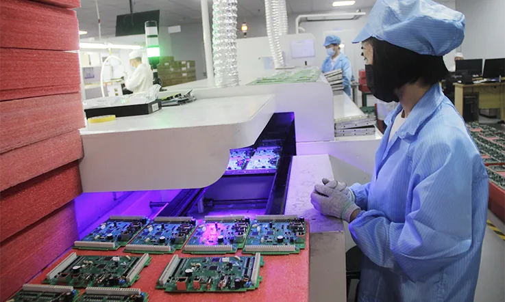
Essential PCB and PCBA File Formats for Assembly Success
When it comes to taking your PCB design to the assembly line, the process is more than just connecting a few components. The right file formats ensure that your design is accurately brought to life, avoiding any costly mistakes along the way. Whether you’re working on single-sided, multilayer, or flexible PCBs, ensuring that the assembly team has the correct files is an absolute must.
In this section, we’re going to break down the most commonly used PCB and PCBA file formats and how they help make the assembly process as smooth as possible. Plus, we’ll explore the files you’ll need to make sure the design-to-assembly workflow doesn’t hit any snags.
BOM (Bill of Materials): Structure and Common Errors
The Bill of Materials (BOM) is the heart of the PCB assembly process. It’s essentially the recipe for your board, listing every single component you need to bring your design to life. Having a well-structured BOM ensures that assembly teams know exactly which parts to use, how many of each, and where they go.
What should a BOM include-
1.Component Details: This includes the part number, description, and value. The more detailed you are, the less likely the assembly team will make mistakes.
2.Quantity: Make sure the quantity of each component is accurate. Ordering too few parts can cause delays, while ordering too many adds unnecessary costs to the production.
3.Supplier Information: Often, manufacturers have specific component suppliers that they prefer working with. Including this information can help expedite sourcing and prevent any issues with parts availability.
4.Footprint and Orientation: For surface-mount components, having the correct footprint and orientation ensures they are positioned accurately on the PCB.
Common BOM errors to watch out for-
| Error | Potential Issue | Solution |
| Missing Components | Delay in assembly due to missing parts | Double-check your list and ensure you have all components specified. |
| Incorrect Part Numbers | Wrong components being ordered | Verify part numbers with the component supplier before finalizing the BOM. |
| Incorrect Quantities | Running out of parts during assembly | Check quantities carefully before submission. Consider adding buffer stock. |
| Incorrect Footprint Information | Misalignment of components during assembly | Verify footprint dimensions and orientations with your design files. |
Pick-and-Place Files: Enabling Automated PCBA Processes
Pick-and-Place files, as the name implies, are packed with all the details that automated assembly machines need to place surface-mount components accurately on a PCB. In the world of PCB assembly, these files are a must-have. They provide precise instructions to the pick-and-place machines, ensuring each component lands exactly where it’s supposed to, every time. Without these files, you risk misplacement or even board failure, which can throw a wrench into the production process. By getting these files right, you’re setting yourself up for a much smoother assembly experience, reducing headaches and saving time in the long run.
What goes into a Pick-and-Place file-
●Component Locations: The X and Y coordinates for where each component should be placed.
●Rotation: The rotation angle for each component. This ensures that passive components are placed in the correct orientation.
●Component Types: Identifying whether a component is a resistor, capacitor, or IC to ensure the machine uses the correct placement head.
How Pick-and-Place Files Improve Efficiency-
1.Reduced Human Error: These files allow machines to handle the placement of parts, which reduces the chance for mistakes compared to manual placement.
2.Faster Production Times: With accurate Pick-and-Place files, your automated assembly lines can work at high speeds, drastically reducing production times.
3.Optimized Component Placement: Automated machines can place components with much more precision than human operators, ensuring that critical components are not misplaced.
For a quick overview, here’s an example of what a Pick-and-Place file might look like:
| Component | X Coordinate | Y Coordinate | Rotation | Reference Designator |
| Resistor | 0.025 | 0.050 | 0 | R1 |
| Capacitor | 0.100 | 0.200 | 90 | C1 |
| IC | 0.300 | 0.400 | 180 | U1 |
Having accurate Pick-and-Place files ensures that assembly is performed quickly, with minimal human error, and that your PCB assembly goes off without a hitch.
Assembly Drawings: Supporting PCB Assembly Accuracy
While Pick-and-Place files guide the assembly machine, assembly drawings serve as a visual reference for the entire assembly process. These drawings provide a clear overview of component placements, soldering points, and instructions. They’re like the blueprints for PCB assembly, ensuring the whole team—whether human or machine—knows where to put every piece of the puzzle.
What should be included in assembly drawings-
●Component Placement: Show the exact placement of all components on the PCB, including passive and active components.
●Soldering Points: Indicate where soldering should occur, both for SMD and through-hole components.
●Assembly Instructions: If there are special assembly steps (e.g., double-sided assembly, thermal management, etc.), they should be included in the drawing to avoid confusion.
Assembly Drawing Example-
| Component | Placement Area | Soldering Method | Special Notes |
| Resistor | Top Layer | Hand-soldered | Ensure correct orientation |
| Capacitor | Bottom Layer | Wave-soldered | Check for polarity |
| LED | Top Layer | Reflow-soldered | Use high-temp solder paste |
These assembly drawings give the assembly team everything they need to ensure accuracy and minimize the risk of assembly defects. Without these detailed instructions, assembly errors can happen—leading to delays, rework, and additional costs.
Best Practices for Preparing PCB and PCBA File Formats
Preparing your PCB and PCBA files thoroughly before submission can greatly impact the efficiency of the manufacturing process. By following best practices, you can reduce the chances of delays, unexpected issues, or unnecessary cost increases. Now, let’s continue to dive deeper into some more specific tips and practices.
Double-Checking Your Files Before Submission
Before sending your files to the PCB manufacturer, take the time to give everything a thorough once-over. Many mistakes occur simply because files weren’t carefully reviewed. Even if you’ve used automated tools or design software, it’s always a smart move to manually check your files to make sure they’re free of errors. Here’s how to properly review and finalize your PCB and PCBA files:
1.Use File Validation Tools: Many PCB design tools like Altium Designer, KiCad, and Autodesk Eagle come with built-in file validation checks that help ensure that your files are ready for manufacturing. However, don’t rely solely on these automated checks.
2.Run Design Rule Checks (DRC): Design Rule Checks (DRC) are a must-do to make sure your PCB design follows the rules your manufacturer has in place. DRC can catch errors like trace widths that are too narrow, or components that are too close together. Running a DRC test ensures your design is DFM-compliant and avoids costly corrections during manufacturing.
3.Cross-Check Your Files Against the BOM and Pick-and-Place Files: One common mistake is submitting a BOM that doesn’t match the components shown in the Pick-and-Place files. This can cause confusion during assembly and lead to mismatches in parts. Always double-check that the part numbers in the BOM align with what’s listed in the Pick-and-Place files.
4.Preview with Gerber Viewers: Gerber viewers allow you to see how your Gerber files will be interpreted by the fabrication machines. This step can catch potential errors before they turn into big problems. You’ll be able to see all the layers clearly, and even verify if everything is aligned as intended.
| Step | Action | Tool/Method |
| File Validation | Run automated checks to detect errors in Gerber, drill, or BOM files | Use design tools’ built-in validators or third-party services |
| Design Rule Checks | Ensure compliance with manufacturing rules | Use DRC tools in your design software |
| BOM & Pick-and-Place Review | Ensure all components are accounted for and aligned | Cross-check BOM and Pick-and-Place files |
| Gerber Preview | Visualize how Gerber files will look during production | Use a Gerber viewer |
Using Cloud-Based Platforms for File Submission
In the modern age of PCB manufacturing, cloud-based platforms offer a convenient way for designers to share files with manufacturers. These platforms allow you to upload Gerber files, BOMs, and other essential files directly to the manufacturer’s system. Using cloud-based tools offers several advantages:
1.Instant File Access and Collaboration-
Once uploaded, both designers and manufacturers can instantly access the files, review them, and even collaborate on any necessary revisions in real time.
2.Automated File Validation-
Many cloud-based platforms offer automated validation tools that immediately flag common issues such as file format mismatches or missing data, helping our PCB designers spot errors early and reduce the need for file re-submissions.
3.Version Control-
Cloud-based platforms provide version control, meaning that designers and manufacturers can track changes in the files and maintain a clear history of all modifications, helping to avoid confusion and delays caused by incorrect files.
Regular Communication with the Manufacturer
In PCB manufacturing, clear communication goes a long way. If you have any doubts about file formats, specs, or best practices, don’t hesitate to reach out to your manufacturer. It’s always better to get the details sorted out early on rather than running into issues down the line. Asking questions upfront can save you a lot of headaches and avoid delays later in the process.
1.Clarify File Requirements-
Every manufacturer might have specific requirements for the file formats they accept. Make sure to verify the details, especially when dealing with advanced formats like ODB++ or IPC-2581. Some manufacturers might require these for complex designs, while others may still rely on traditional formats like Gerber.
2.Ask About File Size Limitations-
Some manufacturers have limits on the size of the files that can be uploaded. Always check if there are any restrictions before submitting large files.
3.Follow Up on File Approval-
Once the files are submitted, follow up with the PCB manufacturer to confirm that they have been properly reviewed and approved. If there are any issues, you want to be the first to know so you can fix them promptly.
Overcoming Common Errors in PCB and PCBA File Formats
When it comes to PCB and PCBA file preparation, even small errors can lead to significant delays or costly mistakes in the manufacturing and assembly process. While modern software tools and file formats are designed to make the process easier, common mistakes still occur. Let’s dive into the typical issues you might face with Gerber files, BOM, and Pick-and-Place files—and most importantly, how to fix them like a pro.
Typical Gerber File Mistakes and Solutions
Gerber files are the bread and butter of PCB manufacturing, but they can sometimes be the source of frustration when they don’t behave as expected. Whether you’re dealing with RS-274X or RS-274D formats, small mistakes can lead to big problems during fabrication. Here’s a breakdown of the most common Gerber file errors and how to troubleshoot them effectively.
1.Missing or Incorrect Aperture Data-
●Problem: If your Gerber file is missing aperture data, or if the aperture definitions are wrong, the manufacturing machine won’t know how to interpret your design. This can result in poor pad sizes or incorrect traces.
●Solution: Double-check the aperture file that accompanies your Gerber file. Ensure that all aperture definitions (for pads, traces, vias, etc.) are present and match the design specifications. Most design tools allow you to preview Gerber files before submitting them to catch such issues early.
2.Layer Misalignment-
●Problem: Layer misalignment is a common issue when Gerber files don’t match the expected physical layers. For example, the copper layer might not line up correctly with the solder mask.
●Solution: Always verify that the layers are properly aligned before submitting. Some Gerber viewers have built-in tools to detect layer misalignment, so take advantage of these to ensure your files are perfectly aligned.
3.Inconsistent Drill Hole Sizes-
●Problem: If your drill file has inconsistent hole sizes or missing holes, it can lead to incomplete drilling during PCB fabrication.
●Solution: Run a drill verification in your design software to ensure all holes are accounted for and that the sizes match your requirements. Then, use a Gerber viewer to verify the final drill file.
| Issue | Potential Cause | Solution |
| Missing Aperture Data | Aperture definitions not included or incorrect | Check and validate aperture file alongside Gerber files |
| Layer Misalignment | Incorrect layering of copper, solder mask, etc. | Use Gerber viewer to align and validate layers |
| Inconsistent Drill Hole Sizes | Drill file inconsistencies or missing holes | Verify and cross-check drill files using verification tools |
Misalignments in BOM and Pick-and-Place Files
A well-structured BOM (Bill of Materials) and Pick-and-Place file can make all the difference when moving from PCB design to PCBA assembly. However, misalignments between these files can lead to confusion during assembly. Here are some common mistakes and solutions to ensure that both files work seamlessly together.
1.Mismatched Component Part Numbers-
●Problem: When the part numbers in the BOM don’t match those in the Pick-and-Place file, the assembly process can get derailed. This often happens if a component is updated in the design but not reflected in the BOM or Pick-and-Place.
●Solution: Always cross-check that every part number in the BOM matches the one in the Pick-and-Place file. If you use automated design tools, they usually allow you to sync your BOM and Pick-and-Place data. If you’re working manually, make sure to run a comparison before finalizing the files.
2.Incorrect Component Placement Data-
●Problem: If the Pick-and-Place file has incorrect placement coordinates or the wrong component rotation angles, the assembly robots could place the components incorrectly, causing design errors.
●Solution: Verify placement coordinates and rotation angles in the Pick-and-Place file. Compare this with the layout on your Gerber files and schematic to confirm accuracy. Running a simulation in Pick-and-Place software will help catch any discrepancies before assembly begins.
3.Missing Components or Values in BOM-
●Problem: Sometimes, components are left out of the BOM or marked incorrectly, leading to shortages or assembly errors.
●Solution: Always ensure that the BOM includes every component listed in the Pick-and-Place file. Automated tools can help compare and match components, but a manual check is also recommended, especially for critical components like capacitors or resistors.
| Issue | Potential Cause | Solution |
| Mismatched Part Numbers | Part numbers in BOM and Pick-and-Place don’t match | Cross-check part numbers in BOM and Pick-and-Place files |
| Incorrect Component Placement | Incorrect coordinates or rotation in Pick-and-Place | Verify placement and rotation using software tools |
| Missing Components in BOM | Components not included or incorrectly marked | Validate BOM for missing components or incorrect values |
Troubleshooting File Issues with CAM Software
The CAM (Computer-Aided Manufacturing) software is designed to help us interpret PCB designs and ensure everything aligns with manufacturing processes. However, issues can still arise that require troubleshooting. Here’s how to address common file issues you may encounter when working with CAM software.
1.Incorrect Drill File Format-
●Problem: Drill files can be misinterpreted by CAM software if they’re not in the expected format, causing errors in the drilling process.
●Solution: Ensure your drill file is in the correct format (commonly Excellon format) and that all tool definitions and coordinates are accurate. You can use CAM software to simulate the drilling process and check for any errors before moving forward.
2.Incompatible File Types-
●Problem: Some CAM software might not support the specific file formats you’re working with (like ODB++ or IPC-2581).
●Solution: Always check the software’s file compatibility before preparing your files. If there’s an issue with file compatibility, most CAM tools will have a conversion tool or suggest a different file format that can be used.
3.Missing Layers or Unreadable Data-
●Problem: If your Gerber files are missing layers or have unreadable data, CAM software will flag these files, resulting in delays in production.
●Solution: Check that all layers are included and readable by the CAM software. Use a Gerber viewer to preview the files and make sure all layers, including copper, solder mask, and silkscreen, are intact.
| Issue | Potential Cause | Solution |
| Incorrect Drill File Format | Drill file not in correct format (e.g., Excellon) | Use compatible drill file format; verify with CAM software |
| Incompatible File Types | CAM software doesn’t support file format | Convert files to compatible formats or use file converters |
| Missing Layers/Data | Missing layers or unreadable data in Gerber files | Use Gerber viewers to verify and correct layer data |
Data Security and Confidentiality in PCB and PCBA File Sharing
Sharing PCB design files and PCBA manufacturing data with suppliers, manufacturers, or design collaborators is a necessary part of the process, but it comes with significant risks. Without proper security measures in place, these sensitive files can fall into the wrong hands, jeopardizing your intellectual property (IP), your client’s trust, and your competitive edge in the market. So, how can you ensure your PCB and PCBA files remain safe throughout the sharing process? Let’s explore best practices to keep your designs secure and confidential.
Protecting Sensitive PCB Design Files from Unauthorized Access
In the world of electronics manufacturing, sensitive data such as Gerber files, schematics, and BOMs hold immense value. These files not only represent your design work but often contain innovative concepts that differentiate your product in the market. Without the right protective measures, these files can be exposed to unauthorized access or data breaches.
1.Encrypt Your Files-
●Why it Matters: Encryption ensures that even if files are intercepted, they cannot be read without the decryption key. This is one of the most effective ways to protect PCB design files from unauthorized access.
●How to Do It: Use file encryption tools to encrypt files before sending them via email or sharing platforms. Popular tools like 7-Zip or WinRAR offer password protection and encryption options to safeguard your files. For cloud storage, use end-to-end encryption (E2EE) to ensure files remain secure throughout the transfer process.
2.Use Secure Communication Channels-
●Why it Matters: Sending files over unsecured channels (e.g., regular email or non-encrypted file-sharing platforms) can expose your data to hackers or other unauthorized parties.
●How to Do It: Always use secure methods such as SFTP (Secure File Transfer Protocol), VPNs (Virtual Private Networks), or secure collaboration tools that offer built-in encryption, like Google Drive with added encryption or Dropbox’s file protection options.
3.Limit Access with Permissions-
●Why it Matters: Limiting access to sensitive files ensures that only the relevant individuals can view or edit your designs, reducing the risk of accidental leaks or misuse.
●How to Do It: Implement role-based access controls (RBAC) and ensure that only those with necessary permissions can access sensitive files. If you’re collaborating with a large team, ensure that everyone’s access is controlled according to their role and involvement in the project.
| Security Measure | Explanation | Best Practice |
| File Encryption | Protects files by converting them into unreadable text | Use 7-Zip or WinRAR for local encryption |
| Secure Communication Channels | Ensures data is transmitted safely over encrypted connections | Use SFTP or VPN for secure file transfer |
| Limit Access | Restricts file access to authorized users only | Use RBAC to assign permissions based on roles |
Secure File-Sharing Tools for Collaboration
Collaboration is necessary in PCB design and PCBA manufacturing, but the tools you choose to share files can make or break your project’s security. When it comes to secure file-sharing tools, you need to strike a balance between usability and data protection. Let’s look at some tools that can help you keep your files safe while working with external manufacturers, partners, or clients.
1.Cloud Storage Services with Built-in Encryption-
●Why it Matters: Cloud storage services like Google Drive and OneDrive can provide convenient access to your files from anywhere, but without proper security, they are vulnerable to unauthorized access.
●How to Do It: Choose a cloud service that offers encrypted file storage and allows for granular permission control. For example, Google Drive allows you to share files with specific users and set expiration dates for file access.
2.File-Sharing Platforms with Audit Trails-
●Why it Matters: An audit trail records all interactions with your files, such as who accessed them, what changes were made, and when they were shared. This becomes super helpful when you’re collaborating with multiple people or working with different manufacturers. It helps you stay on top of things, ensuring you have a clear picture of file activity at all times.
●How to Do It: Platforms like Dropbox Business and Box provide detailed audit logs that allow you to track every file interaction. This gives you a clear picture of who is working on your files and ensures traceability in case any data discrepancies arise.
3.Digital Rights Management (DRM)-
●Why it Matters:Digital Rights Management (DRM) keeps unauthorized individuals from copying, distributing, or altering your files. It’s a must-have security measure when dealing with sensitive intellectual property or confidential designs, ensuring that your work stays locked down and protected while you’re collaborating with external partners or manufacturers. This added layer of defense helps you control who gets access and what they can do with your files, keeping everything under wraps where it belongs.
●How to Do It: Use services like Adobe Document Cloud or Vitrium that allow you to apply DRM policies to your PCB and PCBA files. With DRM, you can restrict downloading, viewing, and printing to ensure your files aren’t misused.
| Tool | Key Feature | Best Practice |
| Cloud Storage Services | Provides encrypted file storage with permission controls | Choose services like Google Drive or OneDrive |
| File-Sharing Platforms | Allows file access tracking via audit trails | Use Dropbox Business or Box for detailed logs |
| Digital Rights Management | Prevents unauthorized file copying or modification | Apply DRM policies using Adobe Document Cloud |
Safeguarding Intellectual Property (IP) in PCB Design and Assembly
Your PCB designs represent not just your engineering effort but also your intellectual property (IP). IP theft or mismanagement of these files can have dire consequences, especially in a competitive market. Whether you’re working with external manufacturers or internal teams, here’s how to ensure your IP stays safe.
1.Non-Disclosure Agreements (NDAs)-
●Why it Matters: NDAs are legal contracts that protect the confidentiality of sensitive information. If you’re sharing PCB design files with third-party manufacturers or collaborators, an NDA is a must to legally bind them to confidentiality.
●How to Do It: Before sharing any design files, ensure that all parties involved sign a Non-Disclosure Agreement. This agreement should specify how the files can be used, who owns the rights to the designs, and how the data will be protected.
2.Track Changes and Versions-
●Why it Matters: Keeping track of design changes through version control safeguards your work while providing a clear roadmap of who made each tweak along the way. Therefore, tracking design changes ensures you know exactly who contributed to each revision of the file.
●How to Do It: Use version control software such as GitHub for PCB design files or Project Management Tools like Jira to keep track of who made changes and when. This helps prevent confusion or disputes over IP ownership.
3.Watermarking Files-
●Why it Matters: Watermarking files adds an extra layer of identification to your designs. This is particularly useful when sharing designs with multiple collaborators or external manufacturers to ensure your IP remains identifiable.
●How to Do It: Use watermarking software to add invisible watermarks to your PCB design files. Some ECAD software also provides built-in watermarking features, allowing you to mark designs without altering the file structure.
| IP Protection Strategy | Explanation | Best Practice |
| Non-Disclosure Agreements | Legally binds parties to confidentiality regarding sensitive data | Have NDAs signed before sharing any files |
| Track Changes and Versions | Ensures all modifications are attributed to the correct person | Use GitHub or Jira for version control |
| Watermarking Files | Adds invisible markers to identify files as proprietary | Use watermarking software or built-in features in ECAD tools |
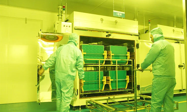
Why Choose Us Become your PCB Manufacturer and PCBA Supplier

JarnisTech Offer PCB and PCB Assembly One-stop Services
At JarnisTech, We are focused on quality and provide the full spectrum of PCB services, such as fabrication, procurement and assembly. It is easy to have your PCB project done by offering a one-stop solution as well as a wide range of tools. Explore our online resources for free, or get in touch with our experienced support team to get help at any point in the project.
What Makes JarnisTech Stand Out?
1.One-Stop PCB and PCBA Services-
From prototyping to full-scale production, JarnisTech has you covered. We specialize in PCB fabrication, component sourcing, and assembly services—all designed to meet the exacting standards of modern manufacturing. This one-stop approach saves you time and minimizes errors caused by working with multiple suppliers.
2.Tailored Solutions for Every Industry-
Whether you’re building PCBs for medical devices, aerospace systems, or consumer electronics, we understand the unique challenges of your industry. Our experienced team collaborates with you to deliver products that meet your specifications and exceed your expectations.
3.User-Friendly Tools and Resources-
We know your time is valuable. That’s why we’ve developed online tools and resources that make submitting your PCB design, BOM, and assembly requirements as easy as pie. If you ever hit a snag, our support team is just a message away, ready to lend a hand.
How to Get Started with JarnisTech?
Getting started is a breeze. If your design files and BOM are ready, head to our Contact Us page to submit your project details. Not sure where to begin? No sweat—our team will guide you through the process and help refine your specifications to achieve the best results.
We’re committed to making your journey with JarnisTech smooth and hassle-free. Take the leap today, and let us help you bring your project to life!


