
As electronic devices continue to demand higher performance and smaller footprints, High-Density Interconnect (HDI) PCBs have become indispensable in pushing the boundaries of modern technology. By offering increased wiring density, reduced size, and enhanced electrical performance, HDI PCBs are powering innovations across industries like automotive, aerospace, and medical electronics. This article dives deep into HDI advancements, practical design considerations, and tailored applications across various industries. Whether you’re optimizing multilayer designs or evaluating cost-effective manufacturing strategies, this resource equips you with the insights needed to harness the full potential of HDI PCBs. Stay ahead in the competitive electronics arena with cutting-edge HDI solutions tailored for your industry!
Comprehensive Overview of HDI PCB Technology
HDI PCBs are at the cutting edge of modern electronics, pushing the limits of size, speed, and performance. These advanced circuit boards are designed to meet the increasing demands of today’s high-tech applications, such as 5G, artificial intelligence, and automotive systems. This section will delve into the key features and manufacturing differences between HDI and traditional PCBs, shedding light on their impact in the world of electronics.
Key Features of HDI PCBs
HDI PCBs are designed for high-performance applications where space constraints demand a compact yet powerful solution. Their distinct features, including high-density connections and miniaturized layouts, allow for efficient and reliable performance in cutting-edge electronics. These boards are commonly found in mobile devices, medical tech, and other electronics where reducing size without sacrificing speed and functionality is necessary.
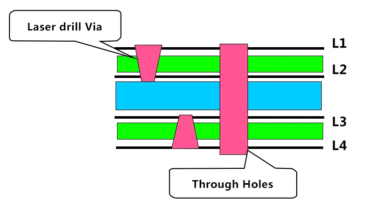
Microvias, Blind Vias, and Buried Vias-
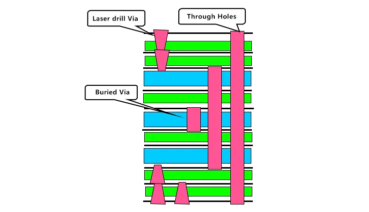
HDI PCBs are distinguished by their use of microvias, blind vias, and buried vias. These vias help achieve high-density connections and compact circuit layouts. Microvias support tight routing, facilitating the miniaturization of circuits in space-limited applications. Blind vias connect outer layers to internal layers without going through the board entirely, conserving space while maintaining connectivity. Buried vias, located within the internal layers, further optimize space usage. Together, these features enable HDI PCBs to meet the growing demand for smaller, faster, and more reliable electronic devices.
●Microvias are tiny holes drilled using laser technology, enabling the connection of multiple layers of a PCB in a very small area. These microvias can reduce the overall size of the board while maintaining effective signal paths.
●Blind vias connect external layers to one or more inner layers but do not extend through the entire PCB. This reduces the need for large, complex vias, further compacting the design.
●Buried vias connect internal layers and are not visible from the outer layers. These vias help in reducing the complexity of the surface layout and contribute to the board’s compact nature.
High Signal Routing Density and Miniaturization-
HDI PCBs excel at transmitting high-speed signals with minimal disruption. Through the use of microvias and advanced stack-up methods, these boards can increase signal density without losing signal integrity. This feature is especially beneficial in industries like 5G communications and automotive systems, where compact designs demand high data transfer capabilities.
Furthermore, HDI PCBs support miniaturization, They allow more components to fit into smaller spaces, which is extremely beneficial in industries where space is limited but functionality must remain high.. These boards can integrate more components into a smaller footprint, enabling the development of smaller, more efficient electronic devices.
Table: Key Features of HDI PCBs-
| Feature | Description | Benefits |
| Microvias | Tiny vias for high-density interconnections. | Enables compact designs and efficient use of space. |
| Blind Vias | Vias that connect outer layers to internal layers, without passing through the entire PCB. | Saves space and enhances signal integrity. |
| Buried Vias | Vias connecting internal layers only, not visible from the surface. | Reduces surface complexity and maximizes real estate. |
| High Signal Density | Ability to route numerous high-speed signals with minimal interference. | Critical for fast, high-performance applications. |
| Miniaturization | Compact design that allows integration of more components in smaller areas. | Supports smaller, more efficient products. |
Difference Between HDI and Traditional PCBs
While HDI PCBs offer numerous advantages, it’s important to understand how they compare to traditional PCBs in terms of manufacturing processes, capabilities, and applications. Below, we break down the key differences and their implications for electronics design.
Manufacturing Process Comparisons-
●Traditional PCBs are typically produced using simpler techniques, such as drilling larger vias and using more conventional layer stacking. These boards are suitable for less complex applications but cannot handle the high-density requirements of modern, performance-driven electronics.
●HDI PCBs, on the other hand, employ advanced manufacturing techniques like laser drilling for microvias, sequential lamination, and stacked vias. These methods allow for higher density interconnections and enable the creation of more complex circuits in less space.
The key difference here is the level of complexity in the manufacturing process. HDI PCBs require advanced equipment and more precise processes, which increases production costs but results in far superior performance and miniaturization.
Advantages in Compact and High-Performance Electronics-
Traditional PCBs are designed to handle fewer layers and lower-density routing, which limits their ability to meet the demands of cutting-edge applications such as 5G, AI, and automotive systems. In contrast, HDI PCBs can support:
●Higher layer counts: Allowing for more circuits to be packed into a smaller space.
●Improved signal integrity: Microvias and buried vias help minimize signal degradation and interference, ensuring the integrity of signals in high-speed, high-frequency applications. By incorporating these advanced via technologies, circuit boards can handle faster data transfer with less disruption, making them ideal for demanding applications like telecommunications and high-performance computing.
●Reduced size and weight: By integrating more components in a compact form, HDI PCBs enable smaller, lighter devices without sacrificing performance.
Table: HDI vs Traditional PCBs-
| Feature | HDI PCBs | Traditional PCBs |
| Layer Stack-Up | Complex multi-layer designs, sequential lamination. | Simpler designs with fewer layers. |
| Via Types | Microvias, blind vias & buried vias for higher density. | Through-holes and larger vias. |
| Signal Routing Density | High-density, efficient routing for high-speed signals. | Limited by larger vias and fewer routing paths. |
| Miniaturization | Compact designs, integrating more components in less space. | Larger, bulkier designs with fewer components integrated. |
| Manufacturing Complexity | Advanced processes, including laser drilling and stacking vias. | Simpler processes, using standard drilling and lamination techniques. |
The Different Types of HDI PCB Stack-ups
1+N+1 – Printed circuit boards contain 1 build-up of high-density interconnect layers.
HDI PCB (1+N+1)
Features:
● Copper-filled via.
● This is suitable for BGAs with lower I/O counts.
● Outstanding mounting stability and reliability.
● Surface treatment and material that is qualified for Lead-free processes.
● Microvia, fine line and registration technologies capable of 0.4 mm ball pitch.
● Application: Mobile phone, UMPC. MP3 Player. PMP. GPS. Memory Card.
1+N+1 HDI PCB Structure
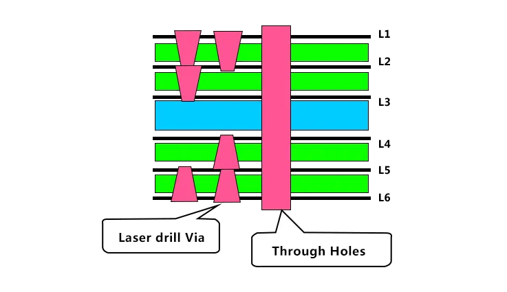
I+N+I (I≥2)–There are two or more layers of high-density interconnections on a printed circuit board. Different layers of microvias can be staggered or stacked.
HDI PCB (2+N+2)
Features:
● Copper-filled via.
● Capabilities for thin boards.
● Complex design increase more routing density.
● It is suitable for BGAs with a smaller ball pitch and higher I/O count.
● Signal transmission performance is improved by using lower Dk/Df materials.
● Application: Mobile phones, PDAs, UMPCs, Portable game consoles, DSCs, Camcorders.
I+BN+i (I≥2)-Includes Buried Vias
Any layer HDI – The layers of a PCB all feature high-density interconnections, which allow conductors on any layer to be freely interconnected using copper-filled stacks of microvias.
ELIC (Every Layer Interconnection)
Features:
● Excellent electrical characteristics.
● Copper-filled vias provide greater reliability.
● Every layer via structure maximizes design freedom.
● Cu bump and metal paste technologies are available for extremely thin boards.
● Application: Mobile phone, UMPC and MP3, PMP. GPS, Memory card.
Advanced HDI PCB Design Techniques
HDI PCB design isn’t just about making things smaller or faster—it’s about doing so without compromising performance or reliability. Achieving this balance requires meticulous attention to detail, cutting-edge technology, and effective collaboration between design and manufacturing teams. These advanced techniques pave the way for creating robust, high-performance boards.
Optimizing Layer Stack-Up in HDI PCBs
Layer stack-up is one of the foundational elements of HDI PCB design. It’s not just about stacking layers for the sake of it—each layer has a specific job to do, and how you stack them impacts signal integrity, power delivery, and overall manufacturability.
Balancing Signal Layers, Power Planes, and Ground Planes-
In a multi-layer HDI PCB, it’s essential to strike the right balance between signal layers and power/ground planes. Signal layers need to be carefully positioned to minimize cross-talk, while power and ground planes should be strategically placed to maintain stable voltage levels throughout the board. The proximity of ground planes to signal layers can greatly affect impedance control and reduce the likelihood of signal interference.
●Optimal Power Delivery: Power planes are often separated from the signal layers by at least one or two ground planes to ensure stable delivery of power. This helps reduce the noise from high-frequency signals affecting the power distribution network (PDN).
●Minimizing Layer Count: Minimizing the number of layers used in a design can reduce cost and complexity. However, balancing fewer layers with adequate signal integrity and power delivery remains a challenge.
Sequential Lamination in HDI PCBs-
Sequential lamination is a method of creating HDI PCBs where layers are built up step-by-step. This technique is often used when designing complex boards that cannot be fabricated in a single lamination cycle due to space limitations or the need for microvias.
●Multiple Lamination Cycles: Sequential lamination enables the creation of stacked vias and microvias in HDI designs. However, this process introduces challenges in alignment and requires precise control over the lamination parameters to ensure that the vias and layers bond correctly.
●Cost vs. Performance: While sequential lamination increases the cost of manufacturing, it allows designers to pack more functionality into a smaller space, making it indispensable for applications like mobile devices, wearables, and automotive electronics.
Table: Layer Stack-Up Considerations in HDI Design-
| Factor | Best Practice | Impact on Performance |
| Signal Layer Position | Should be close to ground planes | Reduces noise and crosstalk |
| Ground Plane Proximity | Should be as close to signal layers as possible | Enhances signal integrity |
| Power Plane Placement | Should be stable and well-aligned with PDN | Ensures consistent voltage delivery |
| Sequential Lamination | Use when more layers are needed for microvia stacking | Enables miniaturization but increases cost |
Stack it right! Maximize your design’s performance by thinking through every layer—your signal integrity depends on it!
The Role of Via-in-Pad Technology in HDI PCBs
In HDI PCBs, space is at a premium, and designers often turn to via-in-pad technology to maximize every square inch. By placing vias directly within the component pads, this approach helps create denser designs, optimizing the board’s real estate. However, while this method offers great advantages in terms of space efficiency, it also comes with challenges, such as potential issues with soldering and via filling that need careful consideration to ensure reliable performance.
Space-Saving and Miniaturization-
The main benefit of via-in-pad technology is its ability to maximize space efficiency. By positioning vias directly within component pads, we can fit more components into a smaller area, which is especially useful for compact electronics like smartphones, wearables, and IoT devices. This innovation helps meet the growing demand for smaller, lighter devices without compromising on performance.
●Microvias for Compact Designs: Microvias are often used in via-in-pad applications because they require less space and can support finer-pitch components. These microvias can be drilled with laser technology for high precision, minimizing board size while maintaining high-density interconnections.
Challenges: Solderability and Void Prevention-
One of the most significant issues with via-in-pad technology is the challenge of solderability. When vias are placed in pads, the solder can flow into the via, causing voids and compromising the electrical and mechanical connection.
●Solutions for Solderability: we can mitigate this issue by using via fill or via plug processes, where the vias are filled with conductive or non-conductive material to prevent solder from flowing into the via. Using filled vias in the design also enhances the mechanical integrity of the board, ensuring that the pads stay intact and do not separate over time.
Table: Via-in-Pad Technology in HDI Design-
| Factor | Considerations | Impact |
| Miniaturization | Allows more components in less space | Enables high-density designs |
| Soldering Challenges | Requires filling vias to avoid solder voids | Ensures reliability and reduces defects |
| Manufacturing Complexity | Increases complexity due to via filling or plugging | May add cost but improves design capability |
DFM (Design for Manufacturing) Guidelines for HDI PCBs
DFM is all about making the design process smoother by ensuring that the design can be manufactured easily, accurately, and cost-effectively. It’s not just a nice-to-have—it’s a must in the world of HDI PCB production, where the margin for error is razor-thin.
Design Collaboration Early in the Process-
One of the best practices for HDI PCB design is involving the manufacturer early in the design phase. This allows the manufacturer to provide feedback on how the design will be fabricated, identifying potential issues with trace width, via sizes, and material choices before they become problems.
●Optimizing for Fabrication Capabilities: Designers need to be aware of the manufacturing constraints related to trace width, via size, and layer count. HDI boards often require microvias that must adhere to specific manufacturing tolerances. By working directly with fabricators during the design phase, you can ensure that the design is within the acceptable limits for fabrication and assembly.
Design for Assembly (DFA) Practices-
DFM and DFA go hand-in-hand, and both need to be considered during the design phase. In DFA, the focus is on simplifying the design to reduce manufacturing time and cost. For HDI PCBs, this includes reducing the number of vias, simplifying trace routing, and ensuring that components are placed in a way that is easy to solder and assemble.
●Minimizing Layer Count: Reducing the number of layers in an HDI design may seem counterintuitive, but when feasible, it can significantly reduce manufacturing time and costs. More layers mean more steps in the fabrication process and higher chances for errors, so aim to design with simplicity in mind whenever possible.
Table: DFM Guidelines for HDI Design-
| Factor | Guideline | Impact on Manufacturing |
| Early Collaboration | Work with the manufacturer from the design stage | Minimizes design flaws and revisions |
| Simplified Design | Reduce vias and optimize trace widths | Lowers cost and simplifies production |
| Layer Optimization | Minimize the number of layers if possible | Reduces fabrication time and cost |
Key Challenges in HDI PCB Design and Manufacturing
HDI PCB design and production involve a detailed and meticulous process that combines high precision with a deep knowledge of balancing performance, cost, and manufacturability. As technology evolves, so does the challenge of crafting these high-density boards that are fundamental to today’s electronic devices. Achieving the right mix of functionality and manufacturability requires careful consideration of factors like layer count, signal integrity, and the ability to fit more components into compact spaces. In short, while it can be a tough nut to crack, it’s the backbone of modern electronics.
Managing Signal Integrity in HDI PCB Designs
Maintaining signal integrity in HDI PCBs is a fine line to walk. As signal frequencies ramp up, the risk of interference, reflection, and crosstalk increases, threatening to degrade the quality of the transmission. When signals travel at high speeds, they become more susceptible to disruption, and without proper design considerations, the signals can lose their clarity and performance. Balancing these factors while keeping everything running smoothly requires careful planning and expert design techniques. This means paying attention to things like trace routing, spacing, and grounding to keep interference at bay.
Signal Loss and Crosstalk-
At high frequencies, even small variations in trace width or spacing can cause signal loss. Crosstalk between traces is another common problem, especially in tightly packed designs. In a high-speed environment, parasitic inductance and capacitance of the traces can distort the signal, leading to errors and inefficiencies.
Design Practices to Minimize Signal Loss-
●Controlled Impedance Routing: In HDI PCBs, ensuring consistent impedance is a fundamental factor in preserving the performance of high-speed signals. Common configurations like microstrip and stripline are used, and the important task is to properly adjust the trace width, layer arrangement, and dielectric constant. These elements must be tuned to match the desired impedance, which helps avoid issues like signal reflections or interference that can disrupt the functionality of the board.
●Minimizing Noise: The use of ground planes in strategic locations reduces the likelihood of EMI (electromagnetic interference) affecting sensitive signal paths. The closer the ground plane is to the signal trace, the more effective the shielding and noise reduction.
●Differential Pair Routing: When routing high-speed signals, differential pairs are used to ensure the signals arrive at the receiver with a high degree of accuracy. These pairs should be kept at equal lengths and spaced consistently to minimize skew.
Advanced Techniques for High-Speed Design-
●Back-Drilling: This technique involves drilling out unused portions of vias, called “via stubs,” to eliminate reflections that can degrade signal quality.
●High-Frequency Material Selection: Substrates with lower dissipation factors, such as low-loss PTFE (Polytetrafluoroethylene) or Rogers materials, are essential for high-speed signals where signal degradation due to resistance and heat can be a significant problem.
Table: Signal Routing Techniques for HDI PCB-
| Technique | Goal | Impact |
| Differential Pair Routing | Minimize skew and preserve signal integrity | Ensures signals arrive in sync |
| Ground Plane Implementation | Reduce EMI and noise | Improves signal-to-noise ratio |
| Back-Drilling | Minimize via-induced reflections | Reduces signal loss and distortion |
Signal integrity is the lifeblood of high-performance electronics—don’t let your design suffer from weak links!
Overcoming Thermal Management Issues in HDI PCBs
In HDI PCBs, managing heat effectively is a must for ensuring the longevity and smooth operation of the board, particularly in high-power or compact applications. As electronic components continue to shrink, efficiently dissipating heat from tightly packed circuits becomes a bigger hurdle. This challenge requires thoughtful design choices, like using heat sinks or optimizing the board’s layout, to prevent overheating, which can cause performance issues or damage the components.
Thermal Management Challenges-
The density of components on HDI PCBs often leads to localized heat build-up, which can cause components to fail prematurely. The risk of thermal damage increases with the number of power-hungry components placed close together, such as power regulators, microprocessors, and memory chips.
●Efficient Heat Dissipation: One approach is to integrate thermal vias into the PCB design. These vias conduct heat away from the components to the back of the PCB, or even to a dedicated heat sink, thereby preventing excessive temperature rise.
●Embedded Heat Spreaders: For PCBs that require even more advanced cooling, manufacturers use embedded heat spreaders—typically made of copper or aluminum—that are integrated into the PCB stack-up. These spreaders help conduct heat away from the source and evenly distribute it across the board to prevent localized overheating.
Selecting Thermal Materials-
The choice of materials in HDI PCBs directly impacts heat management. Ceramic-filled FR4 substrates are becoming increasingly popular due to their improved thermal conductivity over traditional FR4. For flexible or thinner boards, polyimide-based materials help with better heat dissipation. Metal core PCBs (MCPCBs), used especially in high-power applications like LED lighting, excel at effectively managing heat transfer. These material choices help push the boundaries of device performance, especially in compact, high-power electronics, while preventing overheating and ensuring the longevity of the components.
Thermal Simulation and Analysis-
Advanced thermal simulation tools, such as those offered by ANSYS Icepak and COMSOL, allow engineers to perform simulations of heat distribution across the PCB. These tools provide insights into which areas of the board are prone to overheating and enable designers to optimize component placement and routing to mitigate risks.
Thermal Management Table-
| Technique | Application | Benefit |
| Thermal Vias | Power components, high-performance ICs | Moves heat from components to outer layers |
| Embedded Heat Spreaders | High-power applications | Even distribution of heat, preventing hotspots |
| Material Selection | Power modules, automotive electronics | Enhanced thermal conductivity and heat dissipation |
Minimizing Cost Overruns in HDI PCB Prototyping
In the prototyping phase of HDI PCBs, keeping costs under control is a significant challenge. The intricate nature of HDI designs tends to drive up initial expenses, but with careful planning and smart techniques, these costs can be managed. Employing efficient design practices, optimizing material choices, and working closely with manufacturers can help reduce unexpected expenses. Additionally, simplifying certain aspects of the design without compromising the core functionality can lead to more affordable prototyping. With these methods in place, the prototyping phase can be navigated successfully, allowing developers to balance quality and cost effectively.
Streamlining Design and Prototyping-
Efficient design practices, such as Design for Manufacturability (DFM) and Design for Assembly (DFA), help reduce manufacturing errors and unnecessary rework. Working closely with PCB manufacturers early in the design phase can ensure that the design is optimized for the selected fabrication processes, reducing delays and costs.
●Shared Manufacturing Panels: By combining several different designs on the same PCB panel, we can reduce material waste and optimize panel utilization, significantly lowering per-board costs.
●Iterative Prototyping: Instead of finalizing a design and immediately sending it to full-scale production, many engineers now employ iterative prototyping, where smaller batches are produced and tested to identify any issues before larger, costlier runs are made. Rapid prototyping methods, such as laser direct imaging (LDI) and automated optical inspection (AOI), make this process faster and more efficient.
Prototyping Strategies Table-
| Technique | Goal | Impact |
| Shared Manufacturing Panels | Maximize material usage and minimize cost | Reduces per-board material cost |
| Iterative Prototyping | Early detection of design flaws | Lowers overall prototyping costs |
| DFM and DFA Guidelines | Ensure manufacturability and reduce errors | Shortens prototyping time and cost |
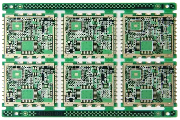
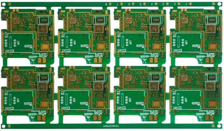
Types of HDI PCBs and Their Applications
HDI PCBs come in various types, each designed to meet specific functional and environmental demands. The choice of HDI PCB type often depends on the application’s complexity, physical constraints, and performance requirements. Here’s a detailed overview of the primary types:
1. Flex HDI PCBs
Flex HDI PCBs are constructed from flexible substrates like polyimide. These materials allow the board to bend and conform to non-planar designs, making them an excellent choice for compact and irregularly shaped devices.
Advantages-
●Highly adaptable to space-constrained designs, enabling dynamic movement.
●Lightweight and durable, ideal for minimizing the footprint of electronic systems.
Challenges-
●Higher manufacturing costs due to complex fabrication processes.
●Requires specialized engineering for precision interconnects.
Applications-
●Satellites: Reducing weight and maximizing performance in space equipment.
●Wearable Devices: Supporting fitness trackers and foldable electronics.
●Medical Tools: Ensuring reliability in flexible diagnostic and monitoring systems.
| Flex HDI PCB | Specification | Details |
| Base Material | Polyimide | Provides flexibility and high heat resistance |
| Thickness Range | 0.05 mm – 0.2 mm | Ultra-thin for compact designs |
| Applications | Satellites, wearables, medical tools | Designed for demanding, space-constrained scenarios |
| Manufacturing Complexity | High | Requires precise wiring and specialized lamination |
2. Rigid HDI PCBs
Rigid HDI PCBs are made with non-flexible materials like FR4. They are designed for mechanical stability, providing reliable performance in applications requiring robust construction.
Advantages-
●High mechanical strength ensures structural reliability.
●Supports high-density routing for complex circuit requirements.
Applications-
●Desktop Systems: Integral to motherboard and GPU designs.
●Industrial Equipment: Ensuring durability under harsh conditions.
●Networking Hardware: Found in servers, routers, and switches.
| Rigid HDI PCB | Specification | Details |
| Base Material | FR4 | Rigid fiberglass for durability |
| Typical Layer Count | 4 – 12 layers | Supports high-density interconnections |
| Heat Conductivity | 0.3 W/m·K | Limited; may require additional cooling solutions |
| Common Applications | Industrial control, servers, networking | Robust design for static, long-term use |
3. Rigid-Flex HDI PCBs
Rigid-Flex HDI PCBs combine rigid and flexible regions, leveraging the benefits of both designs. The rigid section hosts core components, while the flexible part handles interconnections and allows for movement.
Advantages-
●Reduces connectors and cabling, simplifying assembly.
●Performs exceptionally well in dynamic environments.
Applications-
●Aerospace and Defense: Withstands vibration and extreme temperatures.
●Medical Implants: Compact, durable designs for devices like pacemakers.
●Robotics: Modular designs in motion-driven systems.
| Rigid-Flex HDI PCB | Specification | Details |
| Base Materials | Polyimide + FR4 | Combines rigidity and flexibility for hybrid designs |
| Dynamic Bending Life | >100,000 cycles | Suitable for continuous motion applications |
| Thickness Range | 0.2 mm – 2 mm | Offers design versatility across applications |
| Applications | Robotics, medical devices, aerospace | Performs reliably in high-stress environments |
4. Multilayer HDI PCBs
Multilayer HDI PCBs incorporate several layers of substrate and insulation, connected by microvias, blind vias, or buried vias. These designs maximize functionality within a compact footprint.
Advantages-
Excellent signal integrity and reduced cross-talk due to optimized layering.
Enhanced heat dissipation, ensuring stability in high-performance systems.
Applications-
●Medical Imaging Equipment: Used in MRI machines and advanced diagnostics.
●Smartphones: Essential for integrating cameras, sensors, and CPUs.
●Data Servers: Supports intensive processing and data management tasks.
| Multilayer HDI PCB | Specification | Details |
| Layer Count | 6 – 20 layers | Accommodates complex signal routing |
| Thermal Conductivity | 0.5 W/m·K | Enhanced through layered design |
| Microvia Diameter | < 0.1 mm | Enables ultra-high-density designs |
| Applications | Smartphones, servers, medical imaging | Compact and multi-functional integration |
Cost Factors Influencing HDI PCB Production
In HDI PCB manufacturing, cost is always a driving factor. Understanding the elements that contribute to the cost structure will help businesses make informed decisions about procurement, manufacturing, and design. By optimizing these factors, companies can improve their profitability without compromising the quality of the finished product.
Material Costs in HDI PCBs
Material selection plays a big part in determining both the price and performance of HDI PCBs. Not all materials are the same, and choosing the right one is a balancing act between cost and functionality. Let’s dive into the breakdown of how different materials impact your overall costs and how these choices affect your product’s performance. Some materials, while offering higher conductivity or greater heat resistance, can increase the price significantly. Others, while more affordable, might not meet the required specifications for demanding applications. Understanding this trade-off is key to keeping your project within budget while ensuring it meets the performance standards you need.
It’s like shopping for a new car—some options might cost a pretty penny but deliver all the bells and whistles, while others might save you a few bucks but leave you wishing for more performance.
Price Differences Between Standard FR4 and Advanced Substrates-
FR4 is the most commonly used substrate material for PCBs due to its affordability and sufficient electrical properties for many applications. However, when it comes to HDI PCBs, especially in high-frequency or high-performance applications, the choice of material goes beyond FR4.
●FR4: While FR4 is cost-effective, it may not offer the electrical characteristics required for advanced applications like 5G, IoT devices, and automotive electronics. It is often selected for simpler, lower-frequency PCBs, where cost reduction is a priority.
●Advanced Substrates: For HDI PCBs that require superior electrical performance, materials like Polyimide, PTFE (Teflon), and Ceramic are preferred. These substrates can support high-frequency signals with minimal loss, but they come at a higher price point. For instance, PTFE is commonly used in microwave and RF designs due to its low dielectric constant, but it’s significantly more expensive than FR4.
●Impact of Material on Cost: As the material quality improves (e.g., moving from FR4 to PTFE or Polyimide), the production cost rises due to the more specialized fabrication processes, which require different equipment, more time, and more precision. Therefore, selecting a material depends on the project’s specific needs, including its operating frequency and signal integrity requirements.
Table: Material Cost Comparison for HDI PCBs-
| Material Type | Price Range | Applications | Impact on Performance |
| FR4 | Low | Basic consumer electronics | Standard electrical performance |
| Polyimide | High | High-performance electronics | Superior high-temperature resistance and signal integrity |
| PTFE (Teflon) | High | RF and high-frequency devices | Low dielectric loss, ideal for high-speed signals |
| Ceramic | Very High | Aerospace, military, automotive | Excellent signal integrity and thermal performance |
Manufacturing Complexity and Its Cost Implications
Manufacturing complexity is a major factor in the overall cost of HDI PCBs. The more complex the design, the more time, precision, and labor are required to fabricate the board. Understanding these factors can help you navigate cost optimization without cutting corners on quality.
Cost Drivers Like Microvia Density and Layer Count-
One of the primary factors driving up costs in HDI PCB manufacturing is microvia density and the layer count. The more layers a PCB has, the more complex the process becomes, as each layer needs to be laminated and interconnected with vias.
●Microvia Density: HDI designs often require a higher density of microvias to accommodate smaller traces and more compact layouts. The cost of drilling and plating these microvias can quickly add up, especially if the vias are blind or buried. Laser drilling technologies are commonly used to create microvias, but these technologies add to the cost due to the precision and equipment required.
●Layer Count: HDI PCBs often require more layers than standard PCBs due to the need to stack vias and microvias. The more layers your design has, the more time it takes to manufacture, which means higher production costs. However, while a higher layer count increases costs, it can also provide better functionality and miniaturization, which might justify the investment in certain high-performance applications.
Strategies to Optimize Designs for Lower Production Costs-
To reduce the cost of manufacturing HDI PCBs, it’s important to optimizing the design for manufacturability (DFM). Several strategies can help achieve cost savings without sacrificing performance:
●Simplifying Via Structure: Reducing the number of vias, especially blind and buried vias, can significantly reduce manufacturing costs. Opting for through-hole vias instead of blind vias, when possible, can simplify the fabrication process.
●Reducing Layer Count: Minimizing the number of layers can also lower production costs. Using more advanced routing techniques, such as via-in-pad technology and via-fill processes, can help reduce layer count while maintaining the integrity of the design.
Table: Manufacturing Complexity and Its Impact on Cost-
| Factor | Cost Impact | Cost Mitigation Strategies |
| Microvia Density | High due to precision drilling and plating | Simplify via structure, reduce via count |
| Layer Count | Higher costs for multi-layer fabrication | Optimize routing to reduce layers |
| Via-in-Pad Technology | Increases complexity and cost | Use only when necessary for miniaturization |
Cost vs. Quality Trade-offs in HDI PCBs
When it comes to HDI PCBs, there’s often a fine line between cost and quality. The trick is to find that sweet spot where you can achieve the necessary performance without blowing your budget.
Balancing Affordable Pricing with Stringent Quality Standards-
Manufacturers often face a dilemma: how to balance cost and quality. The pursuit of lower costs can sometimes lead to sacrificing performance or reliability. However, cheaping out on the materials, manufacturing process, or testing can lead to long-term issues, such as signal degradation or thermal management failures, which can cost more to fix later on.
●Affordable Pricing: Companies that are just starting or those with tight budgets may lean toward lower-cost materials or opt for offshore manufacturing to reduce expenses. While this can be a short-term solution, it’s important to remember that cheaper materials or manufacturing processes may not stand up to high-performance requirements, leading to higher failure rates down the line.
●Stringent Quality Standards: For mission-critical applications, like medical devices or aerospace technology, cutting corners on quality isn’t an option. These industries demand top-tier materials, cutting-edge fabrication techniques, and thorough testing — all of which drive up the cost. The trick is to establish clear performance goals from the start, so you can identify where to allocate resources and avoid overspending on areas that don’t directly impact the device’s functionality. Being strategic with your choices ensures you’re spending where it matters most.
Tips for Sourcing Reliable Manufacturers-
To get the balance right, selecting a trustworthy manufacturer is key. You want to team up with a company that offers clear and upfront pricing, backed by a solid reputation for delivering high-quality HDI PCBs. Additionally, engaging with them early in the design stage to make sure everyone’s on the same page regarding quality expectations can prevent unexpected cost bumps during production. By working together from the get-go, you can keep the process running smoothly and avoid unpleasant surprises down the road.
Table: Cost vs. Quality in HDI PCB Production-
| Consideration | Lower-Cost Option | High-Quality Option | Impact |
| Material Selection | FR4 or lower-grade materials | High-frequency substrates (PTFE, Ceramic) | Affects signal integrity and reliability |
| Manufacturing Process | Standard vias, less precision | Microvias, via-in-pad, sequential lamination | Increases design complexity and cost |
| Testing and Inspection | Basic quality checks | Extensive testing (ICT, flying probe) | Higher upfront cost, lower failure rates |
Don’t let short-term savings cost you long-term reliability. Know when to spend a little extra to ensure your HDI PCB performs when it matters most!
Innovations Driving HDI PCB Technology Forward
The rapid advancements in HDI PCB technology stem from innovations in precision manufacturing, novel material development, and process automation. These technologies are designed to meet the growing complexity of applications in sectors like AI, telecommunications, and autonomous systems, where performance, reliability, and compactness are non-negotiable.
Laser Microvia Drilling in HDI PCBs
Laser microvia drilling is a cornerstone in HDI PCB manufacturing, enabling intricate designs while maintaining exceptional performance.
Technical Aspects of Microvias-
Microvias are defined by their small size, typically ≤150 μm in diameter, and their function of connecting adjacent layers within the PCB. These vias allow for higher circuit density, reduced inductance, and better signal integrity compared to traditional through-hole vias.
●Depth-to-Diameter Ratio: Maintaining a ratio of ≤1:1 is a must when aiming for solid, long-term reliability. This ensures the design stays balanced and reduces the likelihood of issues popping up later.
●Stacked vs. Staggered Vias: Stacked vias, common in 5G and AI systems, require more precision but offer greater density, whereas staggered vias provide robust connectivity for automotive applications.
Laser Technology in Action-
Advanced laser systems such as UV and CO2 lasers are widely employed for microvia drilling. UV lasers, with their short wavelengths, provide superior control over heat-affected zones, ensuring no thermal damage to adjacent layers. CO2 lasers, on the other hand, are preferred for thicker dielectric materials due to their higher energy output.
| Laser Types | Applications | Advantages |
| UV Lasers | Fine-pitch HDI PCBs | Minimal heat-affected zones |
| CO2 Lasers | Thicker laminates | Higher drilling speeds |
Reliability Testing-
Post-drilling, microvias undergo reliability tests such as thermal cycling (up to 1000 cycles) and CAF (conductive anodic filament) testing to ensure durability in high-temperature and high-humidity environments.
Advancements in HDI PCB Material Technologies
Material science innovations are directly tied to the performance, durability, and application scope of HDI PCBs. Modern materials offer unique properties that cater to the demands of advanced electronic systems.
Material Selection for High-Frequency Applications-
In HDI PCBs used for 5G and radar, materials must exhibit low dielectric constants (Dk) and dissipation factors (Df) to minimize signal loss and phase delay. The following table highlights key materials and their properties:
| Material | Dk | Df | Applications |
| Rogers RO3003 | 3.0 | 0.0010 | High-speed telecom |
| Taconic TLY-5 | 2.2 | 0.0009 | Antenna and RF modules |
| Panasonic MEGTRON6 | 3.4 | 0.0020 | Data centers, AI servers |
Thermal Management Innovations-
HDI designs produce heat due to their compact structures. Ceramic-filled laminates and thermal vias are two major solutions to dissipate heat efficiently.
●Ceramic-Filled Laminates: These materials enhance thermal conductivity while maintaining electrical properties.
●Thermal Vias: By connecting heat-generating layers to thermal pads, they act as heat sinks for improved cooling.
Eco-Conscious Choices-
Halogen-free materials not only comply with environmental standards like RoHS and REACH but also perform reliably in high-frequency applications.
Automation in HDI PCB Manufacturing
Automation in HDI PCB production has shifted the industry towards higher yields, reduced costs, and enhanced precision.
Advanced Robotic Alignment-
Modern robotic systems are engineered to align layers with sub-micron precision, which is especially useful for HDI boards featuring stacked vias and ultra-thin traces. For example, on a 12-layer HDI board, robotics ensure each layer lines up correctly, preventing any mismatch between layers. This precision helps reduce layer-to-layer misalignment, contributing to more reliable and consistent performance in the final product. This type of automated alignment technology is a real advantage in producing complex, high-performance PCBs.
Process Control Systems-
Automated systems monitor and control parameters such as temperature, pressure, and drilling precision. For example:
| Parameter | Automation Benefits |
| Drilling Accuracy | Ensures consistent microvia depths |
| Plating Uniformity | Minimizes voids in copper plating |
| Etching Control | Produces uniform fine-pitch traces |
Inspection and Testing-
Automated optical inspection (AOI) systems and flying probe testers detect micro-level defects like misaligned vias or thin traces, significantly improving product reliability.
Why Choose JarnisTech for Your HDI PCB Fabrication?
JarnisTech is a seasoned provider of high-density interconnect (HDI) printed circuit boards, boasting over two decades of expertise. We’ve cultivated a reputation for delivering top-tier quality alongside competitive pricing and rapid turnaround times. With a focus on global market outreach and adaptability, our approach ensures we can handle even the most demanding HDI PCB requirements.
1. Key Advantages of Partnering with JarnisTech
●Quality Beyond Compare: Our stringent testing protocols ensure every HDI PCB meets precise tolerances and performance standards. From signal integrity to heat resistance, we leave no stone unturned in ensuring you receive reliable boards for even the most challenging applications.
●Competitive and Transparent Pricing: Through optimized processes and a commitment to efficiency, we provide high-value solutions at costs that won’t break the bank.
●Fast Turnaround Without Compromise: Our lean manufacturing systems enable us to handle tight deadlines while maintaining high standards.
●Global Expertise with Local Touch: With customers spanning multiple continents, we’ve mastered the art of balancing local support with global-scale manufacturing resources.
2. Materials for HDI PCB Fabrication
At JarnisTech, we understand that material selection directly impacts the performance and durability of your boards. That’s why we partner with top-tier suppliers like Isola, Nelco, Arlon, Taconic, and Rogers. Our extensive inventory includes laminates with specialized properties for diverse applications.
| Material Properties | Details |
| High Thermal Reliability | Suitable for high-temperature environments, such as automotive and aerospace systems. |
| Ultra-Low Loss | Optimized for high-frequency applications like 5G and advanced communication systems. |
| High-Speed Digital Performance | Ideal for data servers and consumer electronics requiring fast signal processing. |
| Halogen-Free Options | Environmentally friendly, aligning with modern sustainability standards. |
| RoHS Compliant | Meets EU requirements for hazardous substances, ensuring safe and sustainable use. |
| High Tg Lead-Free | Enhanced durability under thermal cycling, suitable for lead-free soldering applications. |
3. Our Manufacturing HDI PCB Circuit Boards Capabilities
| Specification | Details |
| PCB Layers | 4 to 60 layers |
| High-Density Layers | Up to 32 layers |
| Delivery Time | 1 day to 4 weeks |
| Stackup Configurations | 1+N+1, 2+N+2, 3+N+3, 4+N+4…..7N7 |
| HDI Via Options | Blind via, Buried via, Staggered via, Stacked via, Skip via |
| Minimum Laser Drill Diameter | 0.075 mm |
| Final PCB Thickness | 0.15 mm |
| Minimum Trace Width/Space | Flex/rigid-flex PCBs: 1.6 mil / 1.6 mil Rigid PCBs: 2.5 mil / 2.5 mil |
| Minimum Mechanical Drill Diameter | Varies by stackup, includes advanced options such as 7+N+N with copper filling |
| HDI PCB Production Capability | 9000 m² per day |
| Copper Thickness | 100 μm to 125 μm |
| Solderability | >95% (per IPC-TM-650 2.4.14 standards) |
| Surface Finish Options | Selective surface finishes: OSP HASL (SMD: 40 µ to 2000 µ, GND: 30 µ to 800 µ) ENIG (Au: 1 µ to 5 µ, Ni: 80 µ to 200 µ) Immersion Tin (0.8 µm to 1.2 µm) Immersion Silver (0.15 µm to 0.45 µm) Hard Gold Plating (Au: 1 µ to 50 µ, Ni: 80 µ to 200 µ) Peelable Mask (5 mil) Carbon Ink (0.3 mil) |
JarnisTech can manufacture 9000m2 HDI PCBs per day. We provide end-to-end HDI PCB solutions from the initial idea through high-volume production. And we has multiple facilities in China that offer low-volume/high mix PCB manufacturing. At the same time, we also have high-tech capabilities and advanced equipment. Therefore, we can with demanding requirements for medical, defense, aerospace and commercial applications.
FAQ & HDI PCBs
What design software is commonly used for HDI PCB layouts?
Tools like Altium Designer, Cadence Allegro, and Mentor Graphics are widely used for creating precise HDI PCB designs.
How does the choice of laminate affect HDI PCB performance?
Laminate properties like dielectric constant and thermal conductivity directly influence signal integrity and heat management.
Can HDI PCBs support mixed-signal designs?
Yes, HDI PCBs are ideal for mixed-signal designs by offering tight layer control to separate analog and digital signals.
How do stacked and staggered vias differ in HDI PCBs?
Stacked vias are vertically aligned across layers, while staggered vias are offset, affecting manufacturing complexity and cost.
What is the smallest feature size achievable in HDI PCBs?
HDI PCBs can achieve trace widths and spaces as small as 2.5 mils, depending on the manufacturing capabilities.
What is the typical lead time for HDI PCB fabrication?
Production times range from a few days to weeks, depending on complexity and volume.
How do HDI PCBs improve thermal performance?
By integrating thermally conductive substrates and efficient heat dissipation pathways, HDI PCBs manage heat effectively in dense circuits.


