
As circuit boards become more complex and functionality increases, multilayer PCB designs with 16 or more layers are becoming more common. A 16-layer stackup provides additional routing channels and allows for complex power distribution networks to support advanced components with high pin counts. Careful planning is required to maximize the benefits of a 16-layer board while mitigating risks such as crosstalk.
Are you seeking information about the advantages of utilizing a 16-layer PCB stackup or perhaps interested in discovering reputable manufacturers capable of handling your specific project requirements? Look no further, for here we provide comprehensive insights into the benefits offered by 16-layer PCBs.
These intricately designed circuit boards hold immense significance across a wide range of applications, including satellite systems, GPS technology, computer systems, industrial controls, atomic accelerators, and more. Kindly accompany us as we delve into the details of what the 16-layer PCB stackup can offer.
What is a 16 Layer PCB Stackup?
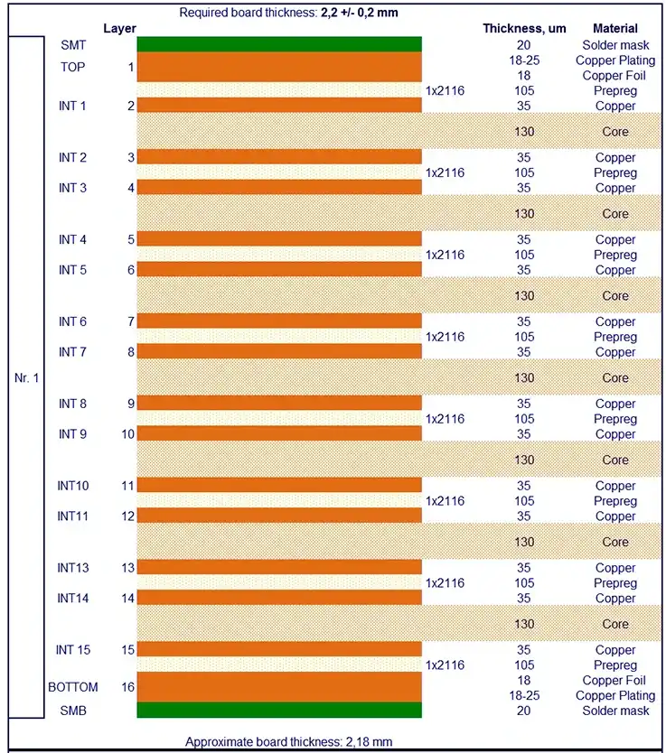
A 16-layer PCB stackup refers to the arrangement of layers in a printed circuit board (PCB) that consists of 16 individual copper layers separated by insulating material. Each layer serves a specific purpose, such as signal routing, power distribution, or ground planes. The stackup configuration determines the electrical and mechanical properties of the PCB.
Typically, a 16-layer PCB stackup consists of alternating signal and ground planes, with internal power planes for distributing power to various components on the board. The stackup may also include additional layers for impedance control, controlled impedance transmission lines, or specific design requirements.
The specific arrangement and order of the layers in a 16-layer PCB stackup can vary depending on the design requirements and the desired electrical performance of the PCB. Designers consider factors such as signal integrity, impedance matching, thermal management, and electromagnetic interference (EMI) mitigation when determining the stackup configuration.
It’s important to note that the selection of the PCB stackup depends on the specific design goals and requirements of the circuit being implemented. The number of layers and their arrangement in the stackup can vary significantly for different applications and designs.
Via Types in 16-Layer PCB Stackups
The number of different types of vias that exist in a 16-layer PCB stackup can vary depending on the specific design requirements and the capabilities of the manufacturer.
Plated Through-Hole (PTH) Vias:
These are the most basic type of vias and are used to establish electrical connections between different layers of the PCB. PTH vias are drilled through the entire thickness of the PCB and are plated to ensure conductivity.
Blind Vias:
These vias connect an outer layer of the PCB to one or more inner layers without passing through the entire board. They are called “blind” because the vias are visible from one side of the board but not the other.
Buried Vias:
Buried vias are similar to blind vias, but they do not extend to the outer layers of the PCB. Instead, they connect one or more inner layers without being visible from either side of the board.
Microvias:
Microvias are very small vias that are typically used in high-density circuit boards. They are much smaller in diameter compared to PTH vias and are often created using laser drilling or mechanical drilling techniques.
Stacked Vias:
Stacked vias are used when multiple conductive layers need to be interconnected. They consist of multiple vias stacked on top of each other, allowing for vertical connections between different layers.
Filled Vias:
Filled vias are typically PTH vias that have been filled with a conductive or non-conductive material to improve the reliability and planarity of the PCB surface. Filled vias are often used in high-frequency applications to minimize signal loss.
What Are Materials Used 16 Layer PCB Stackup?
The selection of materials for a 16-layer PCB stackup depends on various factors such as the desired electrical performance, thermal management, cost considerations, and specific application requirements. Here are some commonly used materials in a 16-layer PCB stackup:
Core Materials:
FR-4 (Flame Retardant-4): A widely used fiberglass-reinforced epoxy laminate with good electrical insulation properties and mechanical strength.
High-Tg (Glass Transition Temperature) FR-4: Similar to FR-4, but with a higher Tg, providing improved thermal stability for applications with higher operating temperatures.
Polyimide: Offers excellent thermal stability and is suitable for high-temperature applications.
Rogers/Isola Materials: Specialized high-frequency laminate materials with low dielectric loss and high electrical performance for RF/microwave applications.
Prepreg Materials:
FR-4 Prepreg: Used for bonding layers together in the PCB stackup, ensuring electrical insulation and mechanical stability.
Polyimide Prepreg: Offers high-temperature resistance and flexibility for applications with demanding thermal conditions.
Copper Foil:
Standard Copper Foil: Typically used for inner layers of the PCB stackup, offering good electrical conductivity.
Rolled Annealed (RA) Copper Foil: Provides better surface roughness and is commonly used for fine-pitch applications and high-frequency circuits.
How to Design a Standard 16-Layer PCB Stack-up?
Designing a 16-layer PCB stackup requires meticulous attention to detail and adherence to specific guidelines. To enhance the design process, the following tips should be followed:
Standard 16 Layer PCB Stack-up:
1.Optimize the board size:
●Determine the required board size based on component mounting needs, considering the number and dimensions of components to be incorporated.
2. Layer design optimization:
●Base the layer design on the signal requirements of the 16-layer PCB stackup, considering factors such as impedance requirements, especially when utilizing fixed or controlled impedance.
3. Via selection optimization:
●Carefully select the appropriate via types for the 16-layer PCB stackup, as this choice significantly impacts manufacturing quality and complexity.
4. Material selection optimization:
●Select materials for each layer of the stackup carefully, considering their individual properties and compatibility with the design requirements.
5. Optimize the board manufacturing process:
●Plan the manufacturing process during the design phase to ensure a successful outcome. Consider factors such as fabrication techniques, assembly processes, and testing requirements.
By following these tips, you can enhance the design process of your 16-layer PCB stackup, resulting in a well-optimized and manufacturable board. Remember to consider the specific requirements of your project and consult with experts or manufacturers to ensure the best results.
Testing Methods for 16-Layer PCB Stackups
It is crucial to recognize the costly repercussions associated with the failure of a 16-layer PCB stackup. Hence, to mitigate such risks, thorough testing of the stackup is essential before its implementation. Several testing techniques can be utilized to ensure the reliability and functionality of the PCB stackup:
1. Functional Testing: This involves verifying the stackup’s overall functionality and performance against the desired specifications. It includes examining the behavior of the circuit under normal operating conditions.
2. X-Ray Inspection: X-ray inspection is used to examine the internal structure of the stackup, ensuring proper alignment of layers, detecting any defects or inconsistencies, and verifying the quality of solder joints.
3. Burn-In Testing: Burn-in testing involves subjecting the PCB stackup to extended operation under elevated temperatures and voltages. This helps identify any potential issues that may arise during prolonged use and ensures the stackup’s reliability over time.
4. Flying Probe Testing: Flying probe testing utilizes automated equipment with movable probes to perform electrical tests on the stackup. It verifies the connectivity of individual circuit paths, checks for open or short circuits, and validates component functionality.
5. In-Circuit Testing: In-circuit testing examines the electrical characteristics of components and circuitry while the PCB is in operation. It helps identify faults, such as incorrect component values or faulty connections, by measuring signals at various test points.
6. Optical Inspection (Automated): Automated optical inspection (AOI) employs high-resolution cameras to inspect the stackup for defects, such as solder bridging, missing components, or misalignment. It enables efficient and accurate inspection of the board’s surface.
By employing these testing techniques, PCB design engineers can ensure the reliability, functionality, and quality of the 16-layer PCB stackup. It is recommended to conduct multiple rounds of testing, including both functional and quality inspections, to minimize the risk of failures and costly consequences.
How Increasing 16 Layer PCB Stackup’s Service Life?
Increasing the service life of a 16-layer PCB stackup involves implementing design and manufacturing practices that enhance its reliability, durability, and performance. Here are some factors to consider for extending the service life of a 16-layer PCB stackup:
Proper Component Selection:
●Choose high-quality components that are suitable for the intended application and have a proven track record of reliability. Consider factors such as temperature range, operating voltage, and environmental conditions.
Thermal Management:
●Incorporate effective thermal management techniques to prevent excessive heat buildup, which can negatively impact component performance and reliability. Use heat sinks, thermal vias, and proper placement of components to optimize heat dissipation.
Signal Integrity Considerations:
●Ensure proper signal integrity by following design guidelines for impedance control, signal routing, and minimizing signal reflections. This helps prevent issues such as signal degradation, cross-talk, and electromagnetic interference (EMI).
Robust Power Distribution:
●Design a well-balanced power distribution network to ensure stable and clean power delivery to all components. Proper decoupling capacitors and power plane designs can help minimize voltage fluctuations and noise.
Environmental Protection:
●Implement proper conformal coating or encapsulation techniques to protect the PCB from moisture, dust, and other contaminants that can lead to corrosion and component failure.
Robust Manufacturing Processes:
●Work with reputable PCB manufacturers who follow stringent quality control measures, use reliable manufacturing techniques, and perform thorough testing and inspection to ensure the highest quality standards.
Design for Manufacturability (DFM):
●Design the stackup with manufacturability in mind, considering factors such as panelization, ease of assembly, and appropriate tolerances. This reduces the risk of manufacturing defects and improves overall reliability.
Proper Handling and Maintenance:
●Handle the PCB stackup with care during assembly, testing, and maintenance processes. Follow proper electrostatic discharge (ESD) precautions and adhere to recommended cleaning and maintenance procedures.
By incorporating these practices, you can enhance the reliability and service life of a 16-layer PCB stackup, ensuring optimal performance throughout its operational lifespan.
16 layer PCB Stackup: Applications
A 16-layer PCB stackup offers increased design flexibility and improved signal integrity, making it suitable for various applications that require complex circuitry and high-performance requirements. Here are some common applications where 16-layer PCB stackups find utility:
●Telecommunications
●Data Storage Systems
●High-Frequency RF/Microwave Systems
●Industrial Automation
●Medical Devices
●Aerospace and Defense
●High-Performance Computing
These are just a few examples of the wide range of applications where 16-layer PCB stackups are utilized. The stackup’s advanced capabilities make it a preferred choice for complex electronic systems that require reliable performance, high-speed data transfer, and precise signal control.
How to Find a Reliable PCB Manufacturer to Make your 16L PCB Stackup?
Collaborating with a reputable 16-layer PCB manufacturer is crucial to ensure the flawless execution of your stackup. It is advisable to select a manufacturer with extensive experience and a team of highly skilled engineers who can meet your specific requirements.
These distinguished manufacturers prioritize the design of the 16-layer stackup to minimize radiation and prevent external noise interference. By employing advanced techniques and expertise, they address issues related to impedance mismatch and signal cross talk, thereby optimizing the performance and reliability of the PCB.
Moreover, it is essential to choose a 16-layer PCB manufacturer that adheres to RoHS (Restriction of Hazardous Substances) compliance standards. This entails utilizing laminate materials that can withstand high temperatures encountered during the assembly process. By ensuring RoHS compliance, these manufacturers contribute to environmental sustainability and the use of safer materials in electronic manufacturing.
When selecting a manufacturer, consider their track record, certifications, and the quality of their manufacturing processes. Look for companies that have a proven reputation for delivering high-quality 16-layer PCB stackups and have a strong commitment to customer satisfaction.
By collaborating with a reliable and experienced manufacturer, you can have confidence in the design and manufacturing of your 16-layer PCB stackup, ensuring optimal performance, reliability, and compliance with industry standards.
Conclusion
With thoughtful stackup design and layout practices, 16-layer PCBs stackup can meet the needs of today’s complex digital systems. By separating critical signals across layers, intelligently using ground and power planes, and managing via transitions, a 16-layer board can provide clean signal transmission at high speeds. Continued innovation in PCB materials and fabrication will further advance 16-layer capabilities for next-generation electronics.


