Designing high-speed PCBs is a journey where one small misstep can throw your entire signal integrity into chaos. Among the gremlins hiding in these designs, crosstalk stands out as one of the most challenging, capable of turning crisp, clear signals into garbled noise. Crosstalk happens when electrical signals in one trace or wire inadvertently interfere with another, leading to unpredictable performance, especially in high-frequency designs.
But crosstalk isn’t an unsolvable mystery—it’s just another challenge to tackle head-on. And when you’re armed with the right knowledge, you can keep those signals behaving themselves like well-trained soldiers marching in line. Let’s dive into how you can reduce crosstalk in your high-speed PCB layout, whether you’re working on your first design or looking to perfect your craft as a seasoned pro.
Understanding Crosstalk in High-Speed PCB Design
What is Crosstalk and Why is it a Problem?
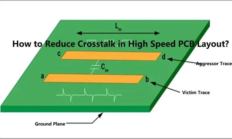
Crosstalk occurs when a signal transmitted on one PCB trace (aggressor) interferes with the signal on an adjacent trace (victim). This interference leads to signal distortion, data loss, and can even crash entire systems in worst-case scenarios. In high-speed PCB designs, where signals are more sensitive to interference, crosstalk can turn into a massive headache if not properly controlled.
So, Crosstalk is an undesirable effect that arises due to the electromagnetic coupling between the traces on a printed circuit board (PCB). Even without physical contact between two traces, a high voltage or current in one trace could induce unwanted effects on another trace. This effect is more pronounced when traces are not adequately spaced apart, as it increases the likelihood of signal interference. The phenomenon can be explained by the generation of an electromagnetic field of a specific intensity whenever a conductor is passed through by an electrical charge. Higher signal speeds (frequencies) further increase the chances of inducing coupling between adjacent signals. There are two different types of coupling: inductive (or magnetic) coupling and capacitive (or electrical) coupling.
Inductive coupling: When designing printed circuit boards (PCBs), it is critical for engineers to consider the impact of inductive coupling. This occurs when current passes through a conductor, such as a PCB trace, generating a magnetic field that can subsequently trigger an electromotive force or voltage in an adjacent trace, following Faraday’s second law of induction. This magnetic or inductive coupling poses a challenge when the induced voltage adversely affects the signal integrity of the same trace. Thus, PCB designers must be cognizant of this effect during the design process.
Parasitic capacity: PCB design engineers must also consider the effects of parasitic capacitance. Alongside the magnetic field generated by current flow, a PCB trace can also generate an electric field that can lead to capacitive coupling upon reaching an adjacent trace. This coupling can impair signal integrity, giving rise to the so-called parasitic capacitance. Thus, during the PCB design process, professionals must be mindful of this phenomenon and proactively take measures to minimize its detrimental impact.
The key challenge lies in the fact that as data speeds increase, the spacing between traces naturally decreases, leading to higher levels of coupling between signals. Now imagine you’re at a crowded party where everyone is shouting to be heard—crosstalk is like the background noise that makes it hard for you to understand the person right next to you. As speeds get faster, that noise becomes harder to ignore.
Types of Crosstalk in PCB Layout
There are two primary types of crosstalk that designers need to watch out for:
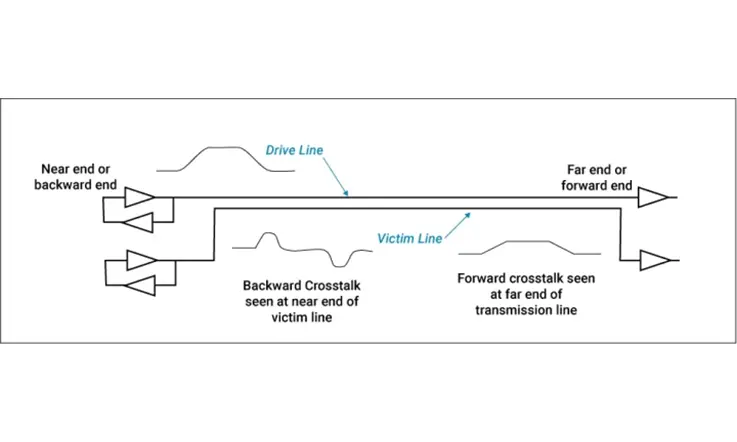
Near-End Crosstalk (NEXT): This occurs when interference is picked up at the end of the trace closest to the aggressor signal source. It’s like your neighbor shouting into your phone conversation.
Far-End Crosstalk (FEXT): This is when the interference is detected at the far end of the victim trace. Picture someone shouting from across the room, and you still catch bits and pieces of their conversation.
Far-End vs. Near-End Crosstalk: Key Differences
Understanding the differences between NEXT and FEXT is critical for designing effective high-speed circuits. NEXT is usually more problematic, as the interference is directly in the receiver’s path, leading to more significant noise and signal distortion. However, FEXT can also create havoc, particularly in longer traces where the noise has more room to accumulate. Knowing when and where each type of crosstalk might occur will help you strategically place mitigation techniques throughout your design.
Differential Crosstalk in High-Speed PCB Designs
Differential signaling is often touted as a robust method for reducing the effects of crosstalk. Unlike single-ended signals that can easily pick up interference, differential pairs work together to cancel out noise, as any interference affects both lines equally. Think of it like two friends having the same conversation amidst chaos—the noise doesn’t throw them off because they’re on the same wavelength.
Common Causes of Crosstalk in High-Speed PCB Layouts
Track-to-Track and Via-to-Track Coupling
The tight spacing between signal traces is a major cause of crosstalk. When traces are placed too close together, the electromagnetic fields from one trace can induce signals on its neighboring traces, resulting in unwanted noise. Via-to-track coupling also contributes to this issue, especially in multi-layer boards where vias may pass through sensitive signal layers.
Now, I know what you’re thinking: “So, why not just space out the traces?” Well, in many cases, you’re working with limited real estate. While increasing trace separation is effective, it’s not always practical, especially in high-density designs where space is at a premium.
Ground Bounce and Power Supply Induced Crosstalk
Ground bounce occurs when the return paths of high-speed signals are shared across multiple traces, causing fluctuations in ground potential. This can lead to significant noise and instability in the circuit. Additionally, the power supply can introduce its own set of problems, particularly when large switching currents are involved. The fluctuation in power supply voltage can couple into nearby traces, further degrading signal integrity.
Effective Crosstalk Reduction Techniques for High-Speed PCB Layout
Proper PCB Trace Spacing and Routing
One thing PCB designers hear over and over again is the importance of trace spacing. It’s not just for neatness—it’s a fundamental strategy to reduce crosstalk. The closer two traces are, the more likely their electromagnetic fields will interact. Increasing the spacing between high-speed traces can lower the amount of coupling and mitigate interference.
Recommended Trace Spacing
A good rule of thumb is to space your traces by at least 3x the trace width to minimize crosstalk. For instance, if your trace is 8 mils wide, spacing it 24 mils away from its nearest neighbor should help keep crosstalk under control. Of course, you’ll need to balance this with the constraints of your board size and routing complexity.
But it’s not just about horizontal spacing. Vertical separation between layers (in multi-layer PCBs) also plays a big role. Increased separation between signal layers can further reduce crosstalk.
We discussed how trace spacing affects crosstalk in high-speed PCB designs. Here’s the refined table that can be used:
| Trace Spacing (mil) | Crosstalk Level | Capacitive Coupling | Inductive Coupling |
| 3 mil | High | Severe | Moderate |
| 5 mil | Moderate | High | Low |
| 10 mil | Low | Moderate | Minimal |
| 20 mil | Minimal | Low | Minimal |
The Role of Differential Signaling in Crosstalk Reduction
Another powerful strategy for controlling crosstalk is differential signaling. Instead of sending a single signal down a trace, you send two complementary signals—one positive and one negative. The idea is that any noise picked up by the two signals will affect both equally, and they’ll cancel each other out at the receiving end. Neat, right?
Differential pairs work wonders, especially in high-speed designs where signal integrity is a top concern. Not only do they minimize crosstalk, but they also provide better immunity to electromagnetic interference (EMI) from other sources.
Routing Differential Pairs
When routing differential pairs, it’s essential to keep the traces running parallel and at the same length. Any mismatch in trace length could result in signal skew, negating the benefits of differential signaling. A common method is to use serpentine routing to ensure both signals arrive at the destination simultaneously.
You can think of differential pairs like a good old-fashioned two-person kayak: they work best when paddling in sync. If one side gets out of rhythm, the whole boat tips, and so does your signal integrity!
Shielding and Guarding Techniques for Crosstalk Prevention
Grounded shields, often referred to as guard traces, can significantly reduce the effects of crosstalk. By placing grounded traces between signal traces, you can effectively block the electromagnetic field from interfering with nearby signals. Think of it like putting up walls between two noisy neighbors—it keeps the noise where it belongs.
For even better results, you can combine guard traces with differential signaling, creating an almost impenetrable defense against crosstalk.
Implementing Via Shielding in High-Speed PCB Designs
Vias can act as unintended antennas, picking up and radiating noise across the board. Shielding vias by placing grounded vias nearby can mitigate this issue. In addition to reducing crosstalk, via shielding can also improve signal reflections and ensure smoother signal transitions across layers.
Advanced Techniques to Improve Signal Integrity in High-Speed PCBs
Using Ground Planes and Return Path Optimization
Ground planes are an essential part of any high-speed PCB design. They not only provide a low-impedance return path for signals but also act as shields against noise. To reduce crosstalk, it’s important to ensure that return paths are kept as short and direct as possible. When return paths are too long, they can create loops that pick up noise from nearby signals.
The Role of Ground Planes in Reducing Crosstalk
Let’s talk ground planes. A properly designed ground plane acts like an invisible shield, blocking interference and giving signals a solid reference point. In high-speed PCB designs, you’ll want to make sure that your ground plane is continuous and provides a short return path for your signals.
Via Stitching and Shielding: Adding vias—small holes in the board that connect one layer to another—can also help reduce crosstalk. By via stitching around critical traces or sensitive signal paths, you can create a barrier that reduces coupling from nearby traces. This technique is especially helpful in boards where you can’t increase trace spacing due to size constraints.
You want those return currents to flow like water down a hill—taking the shortest, most direct path possible to minimize interference.
Impedance Control and Matching for High-Speed Signal Designs
Impedance mismatches can lead to signal reflections, which amplify crosstalk and degrade signal quality. By carefully controlling the impedance of your traces, you can ensure that signals flow smoothly from one point to another without unnecessary reflections. Techniques like impedance matching and controlled impedance routing can go a long way in reducing crosstalk.
High-Density Interconnect (HDI) Technology for Crosstalk Reduction
HDI designs allow for tighter routing without increasing crosstalk. By using microvias, blind and buried vias, and multiple layers, you can pack more signals into a smaller area while still maintaining good signal integrity. However, HDI comes with its own set of challenges, including increased cost and complexity. You’ll need to weigh the trade-offs carefully to see if HDI is the right fit for your design.
Best Practices for Mitigating Crosstalk in High-Frequency PCB Designs
Optimizing Layer Stack-up for Crosstalk Suppression
Layer stack-up plays a crucial role in controlling crosstalk. By carefully designing the order and arrangement of your layers, you can minimize coupling between signal traces. Placing ground planes adjacent to signal layers is one effective strategy for reducing crosstalk in high-frequency designs. Another trick is to use signal routing on alternating layers, which prevents long parallel traces from coupling with each other.
One of the most effective ways to reduce crosstalk in a high-speed PCB design is by optimizing your PCB stack-up. A proper stack-up reduces the risk of coupling by strategically placing signal layers between ground planes or by using shielded configurations.
Layer Stack-up Techniques
In most multi-layer designs, you’ll be dealing with alternating signal and ground planes. Here’s where you can get a leg up on crosstalk:
Use a Ground Plane Between Signal Layers: If you place a ground plane between two signal layers, it acts like a buffer, preventing signals from jumping between traces on different layers.
Route Critical Signals on Internal Layers: Placing high-speed or critical signals on inner layers, sandwiched between ground planes, provides additional shielding, reducing the chances of electromagnetic interference.
For example, let’s consider a 6-layer PCB stack-up. In this configuration, placing ground layers (GND) between signal layers (SIG) can help:
Layer 1: Signal
Layer 2: Ground
Layer 3: Signal
Layer 4: Ground
Layer 5: Power
Layer 6: Signal
With this setup, you’ll reduce field coupling and signal leakage. Keep in mind, though, the dielectric constant of the material between layers matters too. A lower dielectric constant results in better signal isolation, reducing crosstalk further.
Guard Traces: Adding an Extra Layer of Protection
If you’ve got the space, adding guard traces is another effective way to combat crosstalk. A guard trace is essentially an unused trace (often tied to ground) that runs parallel to your signal trace, acting like a physical barrier to block electromagnetic fields.
Best Practices for Guard Traces
When using guard traces, it’s best to place them between critical signal lines. These guard traces should be grounded at multiple points to provide effective isolation. A well-placed guard trace can make all the difference in high-speed designs where trace spacing alone isn’t enough to prevent crosstalk.
EMI Shielding Materials and Techniques
Using specialized materials like conductive coatings and EMI shields can further enhance crosstalk suppression. While these materials come at an additional cost, they can be well worth it for high-speed designs where signal integrity is paramount. Shielding components such as enclosures and ferrite beads can also be used to block EMI at the source.
Using PCB Simulation Tools to Analyze Crosstalk
Simulation tools like Altium Designer or Cadence Allegro can help you visualize and analyze crosstalk before you even create a physical prototype. These tools allow you to simulate signal propagation, identify potential problem areas, and experiment with different mitigation strategies. It’s like taking your PCB on a virtual test drive before hitting the road.
Here’s a pro tip: before you even send your design to the fabricator, use simulation tools to predict and mitigate crosstalk issues. Tools like Altium Designer, Cadence Allegro, and HyperLynx allow you to simulate how signals will behave on your PCB, letting you catch potential crosstalk before it becomes a problem.
How to Use Simulation Tools Effectively?
When running crosstalk simulations, focus on critical nets first—those carrying high-speed or sensitive signals. Use the software to analyze impedance and signal reflection, and tweak your layout until the simulation shows minimal interference.
Simulations give you a sneak peek into how your board will perform in the real world, so it’s worth taking the time to test different configurations and spacing options before committing to a final design.
Examples of Crosstalk Solutions
Nothing drives a point home like real-world examples. Let’s take a look at how one project tackled severe crosstalk issues with creative solutions.
Case Study: Reducing Crosstalk in a High-Density Board
In a recent project involving a high-density server motherboard, the design team faced massive crosstalk issues due to tight routing constraints. Initially, the board experienced significant signal degradation due to near-end crosstalk between adjacent signal layers.
The solution? A combination of increased trace spacing, differential signaling, and shielding with ground vias. Additionally, the team introduced microstrip routing to keep high-speed signals on the outer layers, minimizing interference from internal traces.
By applying these techniques, the team managed to reduce crosstalk to below acceptable thresholds, ensuring reliable signal integrity at operating frequencies exceeding 2 GHz.
Additional Considerations for Reducing Crosstalk in Advanced PCB Designs
When you’re dealing with high-density, high-speed PCB designs, the battle against crosstalk can get intense. And while we’ve covered the most common techniques, there are always other strategies and new technologies you can use to further tighten your designs.
Advanced Materials for Crosstalk Reduction
With the advent of next-generation PCB materials, some designers are choosing to utilize specialized substrates to enhance signal integrity. Materials such as Rogers and Isola have lower dielectric constants and loss tangents than traditional FR4, which can lead to less signal degradation and coupling between traces.
These advanced materials can be particularly beneficial in designs that operate at microwave or millimeter-wave frequencies, where standard materials might not cut it. While these materials come at a higher cost, the trade-off for signal integrity often makes it a no-brainer for high-speed, high-frequency applications.
Future Trends in Crosstalk Mitigation
Innovations in PCB manufacturing and design tools will likely continue to evolve to make crosstalk a more manageable issue. We are already seeing trends toward automated crosstalk management within EDA tools, where layout suggestions are made based on a system’s high-speed requirements. Machine learning algorithms in PCB design could soon predict crosstalk issues before layout is even completed, providing designers with recommendations based on massive datasets from prior designs.
We might also see advances in optical interconnects that could entirely sidestep many traditional signal integrity issues, crosstalk included. By using light instead of electricity to transmit data, optical PCBs could greatly reduce the electromagnetic interference that’s the root cause of crosstalk.
Wrapping Up
Ensuring Signal Integrity in High-Speed PCB Designs
Crosstalk can be a thorn in the side for PCB designers working with high-speed circuits, but with a clear plan and the right techniques, it’s definitely manageable. Keep in mind that the goal is to keep noise at bay, allowing signals to flow smoothly without interference. A combination of good design practices—like proper trace spacing, differential signaling, and smart stack-up choices—can work wonders in reducing crosstalk.
One last tip: always work closely with your manufacturer, especially when tackling complex high-speed designs. They can provide valuable insight into how your design will perform in the real world and offer advice on fabrication techniques to further reduce noise.
Crosstalk doesn’t have to derail your projects. With these strategies in your toolkit, you’ll be well-prepared to handle the challenges of high-speed PCB design and ensure your signals stay squeaky clean, no matter how fast your circuits are running. Just remember: it’s not about perfection, but about knowing how to adapt and fine-tune your design to meet the needs of your specific application.
Key Takeaways
1)Crosstalk in high-speed PCB designs is a significant issue but can be mitigated with proper design strategies.
2)Differential signaling and careful trace routing are crucial techniques for reducing noise.
3)Via shielding, guard traces, and ground planes can act as strong defenses against electromagnetic interference.
4)Simulation tools are your best friend when it comes to predicting and resolving crosstalk before fabrication.
5)Stay on top of your game, and don’t let crosstalk mess with your high-speed designs. You’ve got the know-how, now it’s time to put it into action.
FAQ
Q: How can I reduce crosstalk without adding too much complexity to my PCB design?
A: Start by increasing trace spacing where possible and using differential pairs for high-speed signals. If you’re still seeing interference, introduce ground planes or shielding.
Q: What is the best way to handle crosstalk in multi-layer PCB designs?
A: Use careful layer stack-ups with ground planes between signal layers. You can also route critical signals on internal layers to provide natural shielding from external noise.
Q: How does differential signaling help with crosstalk?
A: Differential pairs help cancel out noise because any interference will affect both signals equally. This helps maintain signal integrity, especially in noisy environments.
Q: Are there any PCB simulation tools specifically for analyzing crosstalk?
A: Yes, tools like Altium Designer, Cadence Allegro, and others allow you to simulate crosstalk and optimize your design before fabrication.