
In today’s digital landscape, where speed, precision, and reliability are demanded at every turn, Impedance Control PCBs (Printed Circuit Boards) are not just a luxury—they are a necessity. Whether you’re a seasoned PCB designer, a manufacturer in the thick of high-speed electronics, or an OEM looking to stay ahead of the competition, understanding impedance control is key. Impedance mismatches can spell disaster for signal quality, introducing noise and reflections that disrupt even the most sophisticated circuit designs.
This guide dives deep into the principles, material selection, stackup design, and manufacturing techniques that define impedance control PCBs. Whether you’re an experienced engineer or exploring this topic for the first time, this comprehensive resource provides actionable insights, practical examples, and industry-proven strategies to optimize your designs and processes. Let’s navigate the complexities of impedance control and unlock the full potential of your PCB designs.
But before diving into the nitty-gritty, let’s first take a step back and explore the origins of impedance control and how it has evolved to meet the demands of modern electronic applications.
The Evolution of Impedance Control in PCB Technology
The need for impedance-controlled PCBs grew out of the requirements of increasingly sophisticated high-speed circuits. As electronic devices began to process more data at higher speeds, many engineers realized that simple traces weren’t sufficient for these complex systems. When the signal paths became too long, narrow, or improperly spaced, signal integrity was compromised, leading to delays, reflections, and noise.
Historical Perspectives on Signal Integrity
When circuit boards were first developed, signal integrity was a secondary consideration at best. Early designs didn’t have the high-frequency demands we face today. However, with the rise of high-speed data transfer technologies—think 5G, the Internet of Things (IoT), and cloud computing—the need for precise control over signal paths became crystal clear. Engineers began to realize that a poor PCB design could cause reflections, signal degradation, and in some cases, complete failure of high-speed transmissions.
It wasn’t until the 1980s and 1990s that impedance control became a recognized standard in PCB design, particularly with the advent of microprocessors and their increasing clock speeds. At that time, designers started using controlled impedance to reduce crosstalk, minimize signal loss, and ensure the integrity of data traveling at ever-increasing speeds.
Key Milestones in Impedance Control PCB Development
The rise of surface-mount technology (SMT) and the demand for smaller, faster devices accelerated the need for impedance-controlled PCBs. Early on, engineers focused on maintaining the correct impedance by carefully designing the width of traces and spacing between them. But that’s only the beginning of the story.
By the 1990s, new manufacturing methods and materials began to surface. Advances in substrates, such as high-frequency laminates, allowed for tighter control over impedance, enabling PCB manufacturers to meet the rigorous standards demanded by high-speed applications. As multi-layer PCBs became more prevalent, PCB engineers had to adapt their impedance strategies to ensure signal integrity across multiple layers, especially for differential pair routing.
Fast forward to the present day, and we now have state-of-the-art tools and simulation software to model and test impedance in real time. No longer do we rely solely on intuition and basic design rules. With modern design tools, we can predict how signals will behave, allowing for much more precise and efficient impedance control.
Why the Future Depends on Controlled Impedance?
The importance of impedance control will only grow. With the advent of 5G networks, autonomous vehicles, and artificial intelligence (AI), the demand for faster, more reliable signal transmission is at an all-time high. The next-generation electronics are pushing the boundaries of what’s possible, and impedance control is at the heart of it.
What Is Impedance Control PCB and Why Does It Matter?
When designing modern printed circuit boards, especially those handling high-speed signals, impedance control is a concept that can’t be ignored. Without it, high-frequency signals could easily experience distortion, signal degradation, or loss, which can lead to errors, data corruption, and inefficient device performance. But what does Impedance Control PCB actually mean, and why is it so crucial in today’s electronic systems?
Definition and Core Concepts of Impedance Control
Impedance control in PCB design is all about understanding how electrical signals behave as they zip through traces on the board. Impedance is a way of measuring how much a signal gets slowed down or resisted due to the resistance, capacitance, and inductance found in the PCB traces. This characteristic has a huge impact on how well signals hold their integrity, especially as they travel at high speeds. If these factors aren’t well-managed, your signals might end up running into some serious speed bumps, causing problems like signal distortion and data loss. Proper impedance control ensures your signals stay on track, keeping everything clear and smooth.
In Impedance Control PCBs, we ensure that these signals face minimal resistance or distortion by designing traces that maintain a specific impedance value. This is especially true for high-speed circuits, where even the smallest impedance mismatch can create serious issues like signal reflections, interference, and data loss. The goal is to keep everything flowing without hiccups—ensuring that signals reach their destination with clarity and precision. Without proper impedance control, your circuit could quickly run into problems, like a bumpy road slowing everything down.
Understanding controlled impedance is more than just preventing issues—it’s about enhancing the efficiency of signal transmission, ensuring your PCB is tuned to perform at its peak, especially in sectors where signal clarity and performance are absolutely non-negotiable. When you fine-tune impedance control, you’re ensuring that signals move like a breeze through the circuit without hiccups, keeping everything in sync.
The Role of Impedance Control in High-Speed PCB Design
Now that we’ve covered the basics, let’s get into the nitty-gritty of how impedance control impacts high-speed PCB design. The key challenge in high-speed electronics is making sure that the electrical signals maintain their integrity as they traverse the PCB. Without impedance matching, signals can bounce off circuit components and traces, leading to unwanted signal reflections that disrupt the normal operation of the device.
To ensure a smooth, uninterrupted signal flow, our PCB designers rely on precise impedance control. This means matching the impedance of the PCB traces with that of the source and the receiver. When done correctly, controlled impedance minimizes the possibility of signal reflection, keeps the signal paths clean, and ensures that your PCB operates at peak performance, even under heavy load and high-speed conditions.
Let’s take a look at the potential effects of impedance mismatch in high-speed PCB designs, and how properly managing impedance can enhance system performance.
| Application | Signal Integrity with Impedance Control | Consequences of Impedance Mismatch | Outcome of Proper Impedance Control |
| 5G Communication Devices | Excellent signal stability, minimal reflection | Significant signal loss and delays in transmission | Faster data speeds, reliable connections |
| Automotive Electronics | Consistent signal transmission without noise | Electrical noise, disruption in sensor data | More reliable vehicle control and safety systems |
| Medical Devices | Clear, uninterrupted signal flow for diagnostics | Potential for false readings and sensor failure | Accurate measurements, improved patient outcomes |
| Consumer Electronics | Stable audio/video signals, high-definition quality | Image distortion, dropped connections | High-quality, uninterrupted media streaming |
The table above shows how different high-speed applications can benefit from proper impedance control. It also highlights the risks involved when impedance mismatching occurs, from communication delays in 5G devices to inaccurate readings in medical equipment. By ensuring impedance is properly matched across the PCB, we can achieve improved performance and reliability, regardless of the application.
Core Principles of Designing an Impedance Control PCB
Designing a printed circuit board with controlled impedance requires a deep understanding of the fundamental principles that ensure signal integrity in high-speed applications. Without precise impedance control, the performance of electronic systems can quickly degrade, leading to signal reflections, loss of data, and unwanted interference. The journey to creating a reliable Impedance Control PCB starts with grasping the core concepts that govern signal transmission across the PCB, such as impedance matching, transmission line theory, and designing for different types of impedance.
In the following sections, we’ll dive into these core principles and explain how they lay the foundation for designing PCBs that function optimally in high-speed environments. Buckle up—because understanding these principles could be a game-changer for your design process!
Understanding Signal Integrity in PCB Design
Signal integrity is a major concern in any PCB design, especially when working with high-frequency or high-speed circuits. Essentially, signal integrity refers to the quality of the electrical signals as they travel through the PCB. When impedance mismatches occur, signals can become distorted, leading to unwanted phenomena like crosstalk, electromagnetic interference (EMI), or even complete data loss.
To maintain strong signal integrity, it’s crucial to manage impedance effectively. A mismatch in impedance along the PCB traces can cause the signal to reflect back toward the source, creating noise that interferes with the desired signal. This can reduce the clarity of the signal and affect the performance of devices—whether that’s a mobile phone, a medical device, or a 5G communication system.
Here’s where impedance matching comes into play. By ensuring that the impedance of the signal trace matches the impedance of both the signal source and receiver, you minimize reflection and reduce crosstalk and EMI. Think of impedance as the “speed bump” on your signal’s journey—if the impedance is well-controlled, the signal travels efficiently without being interrupted.
The Role of Transmission Line Theory in Controlled Impedance
At the heart of controlled impedance design lies the concept of transmission line theory, which helps explain how signals behave as they move along traces. Transmission lines are structures that guide electrical signals, and the traces on your PCB are, in essence, transmission lines. The impedance of these lines depends on their geometry, the material properties of the PCB, and the spacing between conductors.
When designing for controlled impedance, two of the most common transmission line configurations are microstrip and stripline. These configurations define the signal path and influence the impedance profile of the trace.
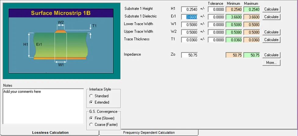
●Microstrip: This is a single trace on the PCB surface, typically surrounded by air. It’s a common choice for surface-mounted PCBs and provides an easy route for signal transmission. The impedance of a microstrip is influenced by its width, the height above the ground plane, and the dielectric properties of the PCB.
●Stripline: A stripline, on the other hand, is embedded within the PCB and sandwiched between two ground planes. This type of design helps shield the signal from external noise and interference. The impedance is largely determined by the trace width, the spacing between the trace and the ground planes, and the dielectric constant of the PCB material.
Both of these transmission lines require careful design to ensure that the impedance remains consistent throughout the PCB. If the trace width or spacing is inconsistent, the impedance can change, leading to signal reflections and degraded performance.
Here’s a simplified comparison of microstrip and stripline designs:
| Transmission Line Type | Configuration | Typical Applications | Impedance Control Considerations |
| Microstrip | Single trace above ground plane | Surface-mounted PCBs, RF circuits | Trace width, height above ground, dielectric constant |
| Stripline | Trace between two ground planes | High-speed digital circuits, multi-layer PCBs | Trace width, spacing, and dielectric constant |
As you can see, both microstrip and stripline designs come with unique benefits and considerations. Depending on your application, choosing the right transmission line structure can make a significant difference in how well the PCB maintains signal integrity.
Designing for Differential and Single-Ended Impedance
When designing Impedance Control PCBs, it’s not just about matching the impedance of individual traces; it’s also about understanding the difference between differential and single-ended impedance. Both types of impedance are used in various high-speed applications, each offering different benefits and challenges.
●Single-Ended Impedance: This type of impedance refers to a single signal trace relative to a reference plane (often ground). It’s commonly used in simpler signal transmission circuits but can be more susceptible to noise and signal degradation over longer distances.
●Differential Impedance: In contrast, differential impedance involves two signal traces that carry complementary signals (positive and negative) in opposite directions. This setup significantly reduces the effect of noise and external interference because the noise tends to affect both signals equally, allowing the receiver to cancel it out. Differential pairs are used in high-speed systems like USB, HDMI, and PCIe.
For proper impedance matching in both single-ended and differential designs, we need to account for factors like trace width, spacing, and the proximity of the reference plane or ground. The goal is to ensure that the impedance of the signal traces aligns with the expected impedance at the source and receiver.
Here’s a quick comparison between differential and single-ended impedance:
| Impedance Type | Signal Configuration | Common Applications | Design Considerations |
| Single-Ended Impedance | Single signal trace vs. ground plane | Low-speed circuits, analog signals | Trace width, distance to ground plane |
| Differential Impedance | Two signal traces (differential pair) | High-speed digital circuits, RF signals | Trace width, trace spacing, reference plane proximity |
For optimal performance, the impedance of both single-ended and differential traces must match the system’s requirements. Failure to do so can lead to signal integrity issues, especially in high-speed or sensitive circuits.
Choosing the Right Materials for Impedance Control PCB
Selecting the appropriate materials for Impedance Control PCBs isn’t just about picking something off the shelf—it’s about choosing the right tools for the job. Whether you’re working on high-speed digital circuits or RF (radio frequency) applications, the material you choose has a significant impact on your design’s overall performance, especially when it comes to maintaining the integrity of the signal and reducing noise interference.
When designing a PCB with impedance control, material selection becomes the cornerstone of signal reliability. So, how do we choose? Let’s break down the top considerations in selecting the best PCB materials for your next high-performance design.
The Importance of Dielectric Constant (Dk) in PCB Design
How Dk influences impedance and signal performance.
The dielectric constant (Dk) of a material plays a fundamental role in determining the impedance characteristics of your PCB. Simply put, Dk describes how much the material can slow down the signal as it passes through it. Materials with a higher Dk tend to have lower impedance, while lower Dk materials result in higher impedance.
In PCB design, impedance matching helps keep signals on track while reducing loss and reflection. When Dk is consistent and well-managed, the impedance across the circuit remains stable, ensuring that your signals travel seamlessly from point A to point B.
Example: If you’re designing for a high-frequency application like RF circuits, a material with a lower Dk (around 2.0-3.0) might be needed to maintain the impedance integrity at the required frequency. On the other hand, for high-speed digital applications like data transmission between microprocessors, a material with a higher Dk is often preferred to balance the electromagnetic interference (EMI) and maintain signal fidelity.
Here’s a breakdown of some popular materials and their Dk values:
| Material | Dk Value | Ideal Use Case |
| FR4 | 4.0-4.5 | General-purpose, low-cost applications |
| Rogers 4003C | 3.38 | High-frequency, RF, and microwave circuits |
| Rogers 4350B | 3.48 | High-speed, low-loss, signal integrity critical applications |
| Isola I-Tera | 3.4 | High-speed digital, telecom, networking systems |
Understanding and calculating Dk is one of the first steps in getting your impedance control design right.
Material Selection for High-Speed and High-Frequency Circuits
Comparing FR4, Rogers, and other advanced PCB materials-
When you’re diving into high-speed or high-frequency circuit designs, picking the right material becomes a big deal. FR4, for example, is the most commonly used PCB material because it’s cost-effective and provides decent performance for a wide variety of applications. However, when you push the boundaries of signal integrity in high-speed designs, FR4 starts to show its limitations—particularly in high-frequency or microwave applications.
Let’s compare some of the top materials you’ll encounter when designing high-speed and high-frequency PCBs:
1.FR4: This material is affordable and widely available, making it ideal for general-purpose applications. However, its high dielectric constant (Dk) and loss tangent may not support ultra-fast digital circuits or high-frequency signals without introducing signal degradation.
2.Rogers PCB Materials (e.g., Rogers 4003C, Rogers 4350B): These materials have low loss tangents and stable dielectric properties at microwave frequencies, making them ideal for RF, telecommunication, and 5G circuits. Rogers materials are great for applications requiring low signal loss and stable impedance.
3.Isola Materials (e.g., Isola I-Tera): Known for high-frequency and high-speed digital applications, Isola materials offer low loss and low Dk values for signal integrity.
4.Panasonic’s Megtron: Offering lower Dk values and improved thermal stability, Megtron is a go-to for high-frequency applications requiring low signal loss and reduced signal reflections.
Here’s a simple table comparing these materials in terms of key characteristics:
| Material | Dk Range | Loss Tangent | Max Frequency | Common Applications |
| FR4 | 4.0-4.5 | Moderate | 100 MHz | Consumer electronics, low-frequency designs |
| Rogers 4003C | 3.38 | Low | 10 GHz | RF, telecommunications, aerospace |
| Rogers 4350B | 3.48 | Low | 20 GHz | High-speed data, telecom, networking |
| Isola I-Tera | 3.4 | Low | 5 GHz | High-speed digital, telecom systems |
| Panasonic Megtron | 3.2 | Low | 25 GHz | Microwave, RF, high-frequency digital |
Choosing the right material here depends heavily on your application requirements. For high-frequency circuits, you’ll typically lean toward Rogers or Isola for their superior signal integrity. But if you’re sticking with low-frequency designs and need to keep the budget in check, FR4 is a reliable pick that won’t drain your wallet.
Balancing Cost and Performance in Material Selection
Strategies for selecting cost-effective yet high-performing materials-
No matter how advanced the technology gets, cost is always a factor. When designing Impedance Control PCBs, you’re often tasked with balancing cost-effectiveness with high performance. For instance, FR4 offers a low-cost solution for general-purpose designs, but for applications like RF or high-speed digital circuits, you’ll need to dig deeper into more expensive, high-performance materials.
Here are a few strategies to strike the right balance:
1.Cost Optimization for Mass Production: If you’re working on consumer electronics where large quantities are required, you may be able to opt for FR4 or Shengyi PCB. These materials offer the cost savings you need without sacrificing too much on performance.
2.Hybrid Material Choices: In complex systems (e.g., automotive electronics, networking equipment), it’s often useful to combine materials for different parts of the circuit. For example, use Rogers or Isola for critical components (like signal traces), and FR4 for less demanding sections (e.g., ground planes).
3.Long-term Reliability Considerations: While high-performance materials like Rogers 4003C or Arlon may have a higher upfront cost, their long-term reliability can prevent failures, saving you money on maintenance, rework, or device returns.
4.Low-Loss Alternatives: If you’re dealing with circuits that don’t demand extreme frequency but still need low-loss properties (such as high-speed digital or mixed signal applications), consider materials like Taconic or Nelco—they can provide great performance at a fraction of the cost of high-end materials.
| Material | Cost | Performance Level | Use Case |
| FR4 | Low | Moderate | Consumer electronics, low-speed |
| Rogers 4003C | High | High | High-frequency, RF circuits |
| Taconic RF-35 | Moderate | Moderate to High | RF applications, telecom, 5G |
| Shengyi PCB | Low to Moderate | Moderate | Mass production, general electronics |
| Arlon 25N | High | High | Microwave, aerospace, high-speed |
By balancing the material cost and performance expectations, you can make well-informed decisions that support your project’s success without overspending on unnecessary high-end options.
PCB Stackup Design for Effective Impedance Control
When you’re designing Impedance Control PCBs, getting the stackup design right can make all the difference. PCB stackup refers to how layers are arranged within a printed circuit board to optimize the signal integrity and electromagnetic compatibility (EMC) of the final product. Getting the stackup design right is like setting the foundation for a building—it supports everything that follows.
In high-speed PCB design, where signals move at lightning-fast speeds, controlling impedance across all layers helps avoid signal reflection, crosstalk, and data loss. . So, let’s dive into how we can design a stackup that ensures your Impedance Control PCB performs as expected in demanding environments.
The Importance of Proper PCB Layer Arrangement
Optimizing stackup for controlled impedance and signal integrity.
The arrangement of layers in a PCB impacts impedance control. When you’re designing a PCB, you’re essentially crafting a path for electrical signals to travel from one point to another. If that path isn’t properly designed, signals can become corrupted, leading to issues like crosstalk, signal reflection, or even complete failure to transmit data accurately.
The most common layers in a PCB stackup are the signal layers, power/ground planes, and dielectric materials. Each of these layers affects the impedance of the circuit and its overall performance. Here’s how to think about each:
1.Signal Layers: These layers carry the high-speed signals and should be carefully routed to maintain controlled impedance. They typically require precise trace widths and optimal spacing from adjacent layers.
2.Ground and Power Planes: Ground planes serve as a reference for the signal and provide a path for current to return, while power planes supply power to the circuit. The distance between these planes and signal layers affects the impedance and signal integrity.
3.Dielectric Material: The material between signal layers must be chosen carefully to ensure consistent dielectric constant (Dk). A lower Dk material allows for better signal integrity and faster signal transmission.
Example: In high-frequency PCB designs, particularly for 5G or RF circuits, positioning signal layers closer to the ground plane helps reduce signal reflection and electromagnetic interference (EMI). The thickness of the dielectric material between these layers also has a substantial impact on impedance control, ensuring that signals remain clear and accurate as they travel through the board. These considerations are integral to optimizing performance in high-speed, high-frequency applications.
Here’s a simple breakdown of the basic PCB layers and their purposes:
| Layer Type | Purpose | Impact on Impedance |
| Signal Layers | Carry the high-speed signals | Directly impacts impedance control |
| Ground Plane | Reference for signal return path | Stabilizes signal integrity, prevents reflection |
| Power Plane | Supplies power to the circuit | Helps in balancing impedance for high-speed signals |
| Dielectric Material | Separates signal and power/ground layers | Affects signal speed, impedance consistency |
Multilayer Stackup Design for High-Speed Impedance Control
Managing impedance across multiple layers in complex PCB designs.
When you move from a single-layer to a multilayer PCB, the complexity of impedance control increases significantly. For high-speed designs, where signals are transmitted at speeds close to the speed of light, even small deviations in impedance can result in large signal integrity issues. To maintain high signal quality and minimal reflection, multilayer PCB stackups need to be designed with meticulous care.
Multilayer designs allow for the inclusion of multiple signal layers interspersed with ground and power planes. These planes provide shielding that helps in minimizing electromagnetic interference (EMI) and also improve thermal management. Signal traces running between these layers must be routed carefully to avoid cross-talk or signal degradation.
Here’s what you need to consider when designing a multilayer PCB with controlled impedance:
1.Layer Pairing: The closer you place signal layers to the ground plane, the better the signal integrity and lower the impedance.
2.Controlled Impedance Routing: To ensure proper signal transmission across different layers, PCB designers often use routing methods like microstrip or stripline. . In microstrip design, the signal trace is placed on the surface, with a ground plane underneath it. In stripline design, the trace is sandwiched between two ground planes.
3.Via Design: The use of vias in multilayer PCBs also requires careful consideration. A poorly designed via can create impedance mismatches or cause signal reflection.
Here’s an example of a multilayer stackup with proper impedance control for a high-speed digital PCB:
| Layer Number | Layer Type | Purpose | Impedance Control Consideration |
| Layer 1 | Signal Layer (Top) | Carries the main high-speed signals | Microstrip design, close to ground plane |
| Layer 2 | Ground Plane | Provides a return path for signals | Low Dk material, reduces EMI, stable impedance |
| Layer 3 | Signal Layer | Carries high-speed signals, possibly differential | Stripline design, minimizes signal loss |
| Layer 4 | Power Plane | Provides power to the components | Helps maintain impedance consistency |
| Layer 5 | Signal Layer (Bottom) | Carries remaining signals | Microstrip design, placed near ground plane |
With multilayer designs, the goal is to create a balanced stackup that maximizes signal integrity while minimizing impedance variations.
Impact of Copper Thickness and Dielectric Thickness
How these factors influence impedance in different stackup configurations.
The thickness of the copper and dielectric materials used in your PCB stackup has a direct impact on the controlled impedance and signal integrity of the board. Copper thickness refers to the amount of copper used in the signal traces and planes, while dielectric thickness refers to the material between the layers that separates the signal traces.
1.Copper Thickness: The thickness of copper impacts the width of signal traces needed to maintain controlled impedance. Thicker copper results in lower trace resistance, but it also requires wider traces to achieve the same impedance.
2.Dielectric Thickness: The thickness of the dielectric material between the signal layers and the ground plane is equally important. Thicker dielectric material reduces the capacitance between the signal and ground, which in turn affects the impedance. The right balance needs to be found to maintain signal integrity without introducing too much attenuation.
Here’s a quick look at how different copper thickness and dielectric thickness affect impedance control:
| Factor | Impact | Best Practice |
| Copper Thickness | Thicker copper reduces signal loss but increases trace width for impedance control | Use for high-power designs or low-speed circuits |
| Dielectric Thickness | Affects capacitance between signal and ground, impacting impedance | Use thinner dielectric for high-speed, low-loss designs |
In high-speed digital circuits or RF applications, precise control of these factors ensures that the PCB meets the required impedance standards and supports reliable signal transmission.
Types of Controlled Impedance in PCBs
In PCB design, controlled impedance ensures that signals flow through the traces without distortion or data loss. The type of impedance selected depends on the kind of signals being transmitted and the complexity of the circuit. Choosing the right impedance helps ensure the circuit operates effectively, especially in high-speed or high-frequency applications.
Let’s take a closer look at the types of controlled impedance you’ll encounter in PCB design.
Single-Ended vs. Differential Impedance
Key differences and use cases in high-speed PCB designs.
When it comes to controlled impedance, one of the first things to consider is whether you’re dealing with single-ended or differential signals. These two signal types require different impedance considerations, and the choice between them will depend on the application.
1.Single-Ended Impedance-
This type of impedance refers to the impedance between a single signal trace and a reference plane (usually a ground plane). For single-ended signals, the impedance is generally determined by the width of the trace, the distance between the trace and the reference plane, and the dielectric material used.
●Use Case: Single-ended impedance is typically used for low-frequency signals or simpler digital circuits where the signal integrity requirements aren’t as strict. You’ll see this in applications like microcontrollers, low-speed logic circuits, and basic digital designs.
●Example: In a typical low-frequency digital PCB, the single-ended impedance might be designed to match a 50-ohm impedance, ensuring the signal can travel from point A to point B without reflection.
2.Differential Impedance-
Differential impedance occurs when a pair of traces carry opposite signals. The impedance between the two traces is measured, and it’s primarily used for high-speed differential signals where the signal integrity is crucial. This is commonly found in differential pair routing, where two traces are routed close together, and the signals are opposite in polarity but equal in amplitude.
●Use Case: Differential impedance is often used in high-speed signal transmission like USB, HDMI, Ethernet, and PCIe. This method helps reduce electromagnetic interference (EMI) and enhances signal quality by using two signals that work together to cancel out noise during transmission.
●Example: In Ethernet PCB design, the differential impedance of the traces typically needs to be controlled to 100 ohms, ensuring that signals are transmitted with minimal interference and signal degradation.
To sum up, single-ended signals are simpler and often used for lower speeds, while differential pairs are more complex and designed for higher-speed, more robust communication, reducing signal degradation over long distances.
Method of Calculation of Impedance Control
Determining the impedance of a PCB is a fundamental task that requires precise methods. Without accurate measurements, achieving reliable performance becomes a challenge. Let’s examine the impedance control methods that are reliable, precise and solid.
1.Smith Chart-
The Smith chart was in use prior to the time computers and EDA PCB design software became commonplace. The chart helps define the relationship between load impedance and source using graphic images. As well as relies on an array of mathematical calculations, it provides you with a trace’s impedance value.
2.Computing Simulation-
Modern software uses sophisticated technology to calculate the impedance of a control. The advantage of this software is that they are able to integrate your design and design concerns into a model to show an almost finished product. But, this kind of software can be expensive to purchase and is used to design a final PCB design.
3.Online Impedance Calculator-
Online calculators are more effective and widely used than design software using impedance control on PCBs. You can determine how to control the impedance of the trace you make using these calculators. These calculators aren’t exactly as accurate as simulators, but they do have a rough estimate to start the process. A few minor tweaks later can keep you in a secure zone as the majority of these calculators are based on standard numbers from the design guidelines of high-speed impedance boards.
The three methods above are a great base for your calculations. Whatever method you decide to use, Compared to not calculating impedance, you’ll start with a set of rules that are safe.
Impedance Control for RF and Microwave Applications
Why precise control is important for wireless and high-frequency systems.
When you’re designing for RF (radio frequency) or microwave applications, impedance control isn’t just a good practice—it’s a requirement. RF and microwave circuits operate at much higher frequencies than typical digital circuits, meaning the challenges related to impedance control are far more pronounced. In these applications, even slight variations in impedance can result in signal loss, reflection, or interference, severely degrading the performance of the system.
1.Impedance Matching-
●Impedance matching is necessary in RF circuits to reduce signal reflections to ensure that signal reflections are minimized. Signal reflections occur when there is a mismatch between the impedance of the signal source, the PCB trace, and the load. This can lead to energy loss, poor signal quality, or even system failure.
2.Use Cases in RF Applications-
●Antenna design: When designing antennas, maintaining consistent impedance across the feedline and the antenna ensures that the signal is transmitted efficiently without unnecessary loss.
●Microwave components: In microwave PCB design, such as for 5G communications or radar systems, it’s essential to ensure that the traces and components are designed to maintain controlled impedance, ensuring efficient transmission of high-frequency signals.
●Example: In 5G PCB designs, the traces must be designed with an impedance of 50 ohms to ensure that signals are transmitted without loss, thus enhancing overall communication performance.
For RF and microwave applications, precise impedance control is non-negotiable. Any deviation in trace width, layer arrangement, or dielectric material can result in significant signal loss, interference, and ultimately, system failure.
Common Impedance Tolerances and Their Applications
Achieving tight tolerances in impedance control PCB manufacturing.
In high-speed PCB manufacturing, achieving the required impedance tolerances is a major aspect of design. Impedance tolerance refers to the acceptable variation from the target impedance. In most cases, a tolerance of ±10% is commonly used, but for some advanced designs, the tolerance needs to be much tighter—sometimes as low as ±2% or even ±1%.
1.Tighter Tolerances for Critical Applications-
For critical high-speed or high-frequency designs, even slight impedance mismatches can cause signal degradation, data loss, or increased EMI. To minimize these issues, tight impedance tolerances are required to ensure signal integrity.
●Use Case: In high-frequency signal processing or RF applications, it’s not uncommon for designers to request an impedance tolerance of ±2% to maintain the quality and reliability of the system. This is often seen in 5G designs, satellite communications, and medical devices that require precise signal fidelity.
2.Achieving Tight Tolerances in Manufacturing-
To achieve the required impedance tolerance, PCB manufacturers use various methods such as advanced routing techniques, controlled copper plating, and consistent material quality. The dielectric constant (Dk) and copper thickness are also factors in keeping the desired impedance steady across the PCB.
●Example: A high-speed digital PCB used for Ethernet or PCIe may require an impedance tolerance of ±5% or better. This is achieved by carefully controlling the trace width, the spacing between traces, and the material properties used in the PCB.
Here’s a simple chart showing common impedance tolerances and their applications:
| Impedance Tolerance | Application | Typical Range |
| ±1% to ±2% | High-frequency RF applications, critical systems | Satellite, 5G, Medical |
| ±5% to ±10% | Standard digital and analog systems | Ethernet, PCIe, USB |
| ±10% | Low-speed circuits, non-critical designs | Basic digital PCBs |
Maintaining tight impedance tolerances ensures that the design operates as expected, without unexpected signal distortion or loss.
Manufacturing Challenges in Impedance Control PCB Production
Creating PCBs with precise impedance control isn’t exactly a piece of cake. It takes a mix of state-of-the-art tech, spot-on calculations, and manufacturing finesse to get it right. Let’s dig into the typical hiccups that can trip up the process and see how modern techniques are flipping the script in PCB production.
Achieving Tight Tolerances in Controlled Impedance PCBs
The fine art of precision in high-speed PCB manufacturing.
In high-speed and high-frequency PCB production, precision isn’t just a recommendation—it’s the cornerstone of successful designs. Tolerances in controlled impedance directly affect the PCB’s performance, and achieving the tight tolerances required for advanced applications involves several factors:
1.Material Consistency: Variations in the dielectric constant (Dk) across the board material can lead to unexpected impedance fluctuations. Using premium, consistent materials like Rogers, Taconic, or Isola laminates helps minimize these risks.
2.Manufacturing Techniques: Achieving precise trace widths, layer spacing, and uniform copper thickness requires highly calibrated manufacturing equipment. Errors in any of these parameters can result in impedance mismatches that affect signal quality.
3.Inspection and Testing: To ensure compliance with design requirements, many manufacturers use advanced impedance testing equipment, such as Time Domain Reflectometers (TDR), to measure impedance values with pinpoint accuracy.
●Example: A high-speed PCIe design might require a differential impedance of 85 ohms ±2%. Achieving such tight tolerances means controlling variables like trace etching depth, copper weight, and material uniformity during production.
Here’s a quick table summarizing tolerance levels and their challenges:
| Tolerance Level | Application | Challenges |
| ±1% to ±2% | High-frequency and RF circuits | Requires precise material and process control |
| ±5% | Standard high-speed interfaces | Balancing cost and precision |
| ±10% | Basic digital designs | Relatively easier to achieve |
Achieving tighter tolerances often requires significant investment in equipment and expertise. However, the results pay off in designs that perform as intended, even under demanding conditions.
Common Issues in Impedance Control PCB Manufacturing
Tackling impedance mismatch, signal loss, and via-related challenges.
Impedance mismatch, signal degradation, and via impedance issues are the trifecta of challenges that engineers and manufacturers face during impedance-controlled PCB production. Here’s a breakdown of these issues and how to address them:
1.Impedance Mismatch-
Mismatched impedance occurs when there’s a discrepancy between the trace impedance and the load or source impedance. This mismatch causes signal reflections, leading to data corruption or degraded signal quality.
●Solution: Impedance mismatch can be minimized by ensuring precise control over design parameters like trace width, spacing, and dielectric thickness. Using advanced simulation tools during the design phase helps predict and mitigate potential mismatches before production.
2.Signal Loss-
Signal loss is another common headache, especially in high-frequency applications where resistance, dielectric loss, and conductor surface roughness can all contribute to attenuation.
●Solution: Reducing copper surface roughness and selecting low-loss materials such as Teflon or PTFE laminates can significantly mitigate signal loss. Additionally, shorter trace lengths and proper layer stackup designs help maintain signal strength.
3.Via Impedance-
Vias introduce discontinuities in the impedance path, which can lead to signal reflections and loss. This becomes especially problematic in high-speed designs, where even minor inconsistencies can throw things off balance.
●Solution: Optimizing via geometry, using back-drilled vias, or employing impedance-matched via designs can reduce the impact on signal quality.
Advanced Techniques for Reliable Impedance Control
Leveraging state-of-the-art tools and processes to ensure top-notch quality.
Meeting the demands of impedance-controlled PCBs requires a mix of advanced technology and meticulous attention to detail. Here are some of the cutting-edge techniques we employ to deliver reliable results:
1.Simulation Software for Pre-Manufacturing Validation-
Tools like HyperLynx, Ansys HFSS, and ADS allow our pcb engineers to simulate and fine-tune impedance parameters before production begins. These tools help identify potential bottlenecks and ensure designs align with manufacturing capabilities.
2.Automated Etching and Lamination Processes-
Automation ensures consistency and precision in processes like trace etching and layer lamination. Automated systems reduce the margin of error, ensuring that the final PCB matches the design specifications.
3.High-Precision Impedance Testers-
Impedance testers, such as Time Domain Reflectometers (TDR), are used to verify that the manufactured boards meet the specified impedance requirements. These tools provide a detailed analysis of the board’s electrical characteristics, ensuring no surprises during deployment.
4.Selective Material Usage-
For high-frequency and RF designs, we often turn to materials with low dielectric loss and minimal variation in Dk. Laminates like Rogers RT/duroid, Isola Astra, and Taconic RF materials are commonly used for these applications.
5.Controlled Impedance Coupons-
During manufacturing, impedance coupons (small test sections) are fabricated alongside the main PCB. These coupons are tested to ensure the impedance matches the desired specifications, providing an added layer of quality assurance.
How to Specify PCB Impedance with JarnisTech?

Defining PCB impedance requirements for manufacturing can seem like a complex task, but with the right approach, you can streamline the process and ensure accurate results. Let’s break down the essential parameters, step-by-step, and offer practical examples to clarify how to communicate these requirements effectively.
1.Target Impedance: The Foundation of Your Design
The first step in specifying impedance is identifying the desired characteristic impedance. This typically depends on the application:
●50 ohms: Common in single-ended signal lines such as USB or Ethernet.
●90–100 ohms: Standard for differential pair applications like HDMI, PCIe, or SATA.
●75 ohms: Often used in RF systems or video transmission lines.
2.Trace Width and Height: The Geometry of Impedance
Impedance is heavily influenced by the dimensions of your PCB traces:
●Trace Width: Narrower traces increase impedance, while wider traces lower it.
●Trace Height (or copper thickness): Thicker copper layers reduce impedance due to lower resistance.
When designing for controlled impedance, tools like online calculators or PCB simulation software can help visualize how changes in geometry affect impedance.
Example Table for Single-Ended Impedance (50-ohm target):
| Trace Width (mm) | Dielectric Thickness (mm) | Copper Thickness (oz) | Impedance (ohms) |
| 0.20 | 0.15 | 1 | ~50 |
| 0.15 | 0.12 | 0.5 | ~52 |
| 0.25 | 0.20 | 1.5 | ~48 |
3.Layer Placement: Context Matters
The arrangement of stackup layers and the positioning of traces significantly influence the impedance values achieved in a PCB design. Controlled impedance traces should be routed near a ground or power plane to maintain consistency. The specific placement affects:
●Microstrip: Traces on external layers above a ground plane.
●Stripline: Traces between two ground planes, offering better shielding but requiring careful layer spacing.
Practical Example: A 4-layer PCB for USB 3.0 could use microstrip routing on the top layer for high-speed signal lines and reserve stripline routing for internal high-speed differential pairs to reduce EMI.
4.Spacing: More Than Just a Gap
Spacing applies to differential pairs and coplanar waveguides, where the gap between traces and adjacent planes impacts impedance:
●Differential Pair Spacing: Tight coupling reduces differential impedance, while wider gaps increase it.
●Coplanar Waveguide Spacing: The distance to nearby ground fills also affects performance.
Differential Pair Design Table (100-ohm target):
| Trace Width (mm) | Spacing (mm) | Impedance (ohms) |
| 0.18 | 0.15 | ~100 |
| 0.20 | 0.10 | ~95 |
| 0.15 | 0.20 | ~105 |
5.Using Tables to Communicate Design Intentions
When specifying impedance requirements to a PCB manufacturer like JarnisTech, clarity is king. Presenting a comprehensive chart that includes impedance targets, trace dimensions, copper thickness, and dielectric properties eliminates ambiguity. Here’s an example of how you can structure this data:
| Parameter | Value/Range | Notes |
| Target Impedance | 50 ohms (single-ended) | USB and Ethernet signal lines |
| Copper Thickness | 1 oz | Ensure uniformity across all signal layers |
| Dielectric Thickness | 0.15 mm | Between signal layer and adjacent ground plane |
| Trace Width | 0.20 mm | Single-ended traces |
| Differential Pair Spacing | 0.15 mm | 100-ohm differential pair (e.g., HDMI) |
So Why Choose Us Manufacturing Your Impedance Control PCB?
Please find the following our manufacturing impedance control PCB capabilities:
| Parameter | Specification |
| Impedance Tolerances | ±5%~±7% |
| Layer Count | 1-46L |
| Maximum Copper Thickness | 20OZ |
| Minimum Trace Width and Spacing | 2.5mil |
| Minimum Via Size for Laser | 0.1mm |
| Minimum Via Size for Machine | 0.15mm / 6mil |
| Base Material | FR-4, High Tg FR-4, Aluminum, Rogers, etc |
| Board Thickness | 0.2-8mm |
| Thickness Tolerance | ≤1.0mm: ±0.10mm, >1.0mm: ±10% |
| PCBA Services | SMD, SMT, DIP Component Assembly |
| Surface Finish | LF HASL, plating hard gold, ENIG, ENEPIG, Immersion Tin, Immersion silver, OSP |
| Certifications | ISO9001, ISO14001, CE, RoHS, UL, IATF16949, ISO13485 |
Controlling PCB impedance is one of the most important concerns and difficult issues encountered when it comes to high-speed PCB development. If you are an impedance-control engineer, you need to know what influences PCB impedance as well as how to calculate the impedance? So, Please feel free to contact us by email and telephone ([email protected], 0086-0755-23034656), let’s talk detail about your impedance control PCB Project!
FAQs on Impedance Control PCBs
How does PCB trace geometry affect impedance?
Impedance is influenced by trace width, spacing, copper thickness, and the dielectric properties of materials. Adjusting these parameters helps achieve the desired impedance.
Can impedance control be applied to multilayer PCBs?
Yes, multilayer PCBs allow more precise control of impedance by layering signal traces between ground and power planes to minimize noise and interference.
What tools are used for calculating controlled impedance?
Specialized software like HyperLynx, Si9000, or Altium Designer includes impedance modeling tools to simulate and calculate PCB trace impedance accurately.
What are common tolerances for controlled impedance?
Typical tolerances range from ±5% to ±10%, depending on the application and the manufacturer’s capability.
Are there specific materials recommended for controlled impedance PCBs?
High-frequency applications often use materials like Rogers, Taconic, or Isola due to their low dielectric constant and stable properties.
What are the main challenges in manufacturing controlled impedance PCBs?
Challenges include maintaining tight tolerances, consistent material properties, and precise trace geometries throughout the production process.


