In the world of technology, electronic devices and advances go hand in hand. As a result, the significance of circuit boards has gained substantial importance, making it an essential aspect that every professional in the electronic industry- including students, engineers, designers, and hobbyists- must grasp. A comprehensive understanding of printed circuit boards is crucial for professionals in the electronic industry, and this article aims to provide a detailed explanation of a vital component of PCB technology- Surface Mount Technology (SMT). By explaining the various useful aspects of SMT in the context of printed circuit boards, electronic industry professionals can upgrade their skills, and keep pace with the rapidly evolving developments in this field.
SMT: Surface Mount Technology
As PCB designers, it is essential to be aware of the technology utilized by printed circuit boards employing surface mount technology. A circuit board employing SMT may or may not have holes on their interior surface. Rather, electronic components are situated on top of copper pads and traces already present on the PCB’s surface.
Thanks to this semi-automated process, manufacturers can generate all the necessary circuit boards for their products within their own facilities. This innovative technology facilitates a straightforward attachment of electronic components to the surface of printed circuit boards in a manner distinctly different from the traditional insertion method employed by manufacturers.
SMT technology provides an alternative to the conventional approach of creating circuit boards that use through holes. Compared to the through-hole technology, SMT addresses several deficiencies and limitations due to its more contemporary iteration. In summary, it is essential for PCB designers to be familiar with SMT to effectively design cutting-edge PCBs that feature surface mount technology.
The Process of Surface Mount PCB Assembly
In the PCB industry, the assembly process for Surface Mount Technology (SMT) involves several crucial steps, with design being the most critical. Prior to beginning the design using Cadstar or Orcad, it is imperative to select the appropriate components. When necessary, alternative software design tools can be utilized. PCB designers should aim to incorporate as many design features as necessary into the PCB to enhance its functionality.
● Once the design and component selection is complete, the PCB data must be sent to the production firm, along with adherence to automation guidelines when procuring components. Crucial specifications to consider for the PCB design include surface treatment, which should be encoded into the appropriate Gerber file format before submission.
● Payment processing will trigger the delivery of package components, usually in reels. It is crucial to avoid loose components as they may require the purchase of particular feeding plates or manual placement, both of which are laborious and time-consuming.
● The next step is to print the solder paste using the appropriate supplies, including the solder paste, printing stencil, and solder paste printer. It is essential to ensure accuracy during this stage to avoid any potential errors that could lead to a disaster in subsequent phases.
● After printing the solder paste, an inspection should be carried out before proceeding to the automatic optical inspection (AOI), first article inspection (FAI), and component placement steps. Upon completion of these stages, the final assembly process is verified using x-rays to ensure that everything was assembled correctly. PCB Industry professionals should be aware of the importance of each step in the SMT assembly process to ensure high-quality end products.
Surface Mount Technology: Advantage
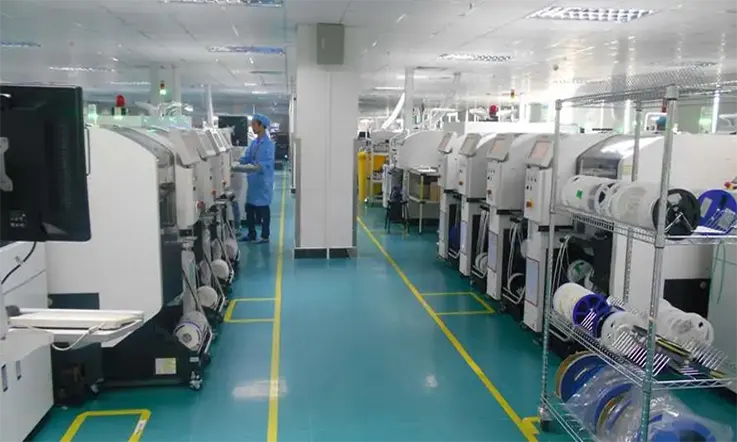
● Automated Assembly: For PCB manufacturers, utilizing automated pick and place equipment is a necessary aspect of the surface mount technology assembly process. This equipment facilitates the installation process of the vast number of surface-mounted components (SMT) on circuit boards, resulting in a highly efficient and precise process. High-volume components, such as passive components, are loaded automatically into the automated SMT machines from a reel. Meanwhile, other components are loaded via trays or tube feeders. This process is markedly different from the traditional plated-through-hole (PTH) components, which require manual assembly. The use of automated equipment in SMT technology enables the manufacturer to achieve high-speed, accurate and cost-efficient production, enhancing product quality and customer satisfaction, and overall profitability.
● PTH Component Commonality: In the electronic industry, surface mount technology parts have proven to be a cost-effective solution due to their smaller size and voluminous nature compared to their plated-through-hole (PTH) counterparts. As a result, SMT components frequently cost less than PTH equivalents, offering manufacturers and customers a more cost-effective solution for their electronic needs.
Moreover, there is a high demand for SMT components compared to through-hole parts, resulting in the availability of these components in the market. The supply chain for surface mount technology components is well-established, making it easier for electronic industry manufacturers to access and procure these crucial components. Overall, the electronic industry has embraced SMT technology due to its cost-effectiveness and supply-chain effectiveness, ensuring the production of high-quality electronics while achieving economic efficiency.
● Size: For designers, surface mount technology offers the benefit of producing components that are more compact than their plated-through-hole (PTH) counterparts, since long leads for insertion and soldering into holes are not necessary. This advantage allows designers to accommodate a greater number of components within a given board space, a crucial consideration when working within constrained board design environments. Such compactness afforded by SMT technology presents a significant opportunity for designers to maximize their board’s functionality while still achieving a high degree of precision and accuracy. Consequently, SMT technology enables designers to achieve greater flexibility when working with board space limitations, enabling them to produce high-quality electronic designs that fulfill their customers’ needs.
● Electrical Performance: The application of Surface Mount Technology (SMT) in printed circuit board (PCB) production has become increasingly prevalent in contemporary times. SMT PCB’s small size allows for the integration of more components while minimizing signal path length, resulting in superior signal integrity and reduced heat output compared to the Through-Hole PCB (PTH). As a result, commercial machinery manufacturers have taken to adopting SMT to fabricate a wide range of PCB devices in convenient packages. This trend fortifies the feasibility and cost-effectiveness of the technology.
Surface Mount Technology: Disadvantages
● Surface Mount Technology (SMT) is a widely used method of PCB assembly that offers improved component placement speed. However, it is not a zero-defect method and presents unique challenges during assembly.
● One of the drawbacks of SMT is that the machinery required for assembly is expensive, leading to a notable initial capital expenditure. While this cost may be offset by reducing the cost of board assembly, it may be challenging for electronic assembly manufacturers working with low-volume prototype boards.
● Additionally, SMT increases the likelihood of component misalignment compared to Through-Hole Technology (THT). This is because, with THT, the leads are inserted through the holes in the circuit board, ensuring perfect alignment of the components. However, with SMT, extra care must be taken during assembly to avoid misalignment.
SMT Manufacturing Process:7 Steps
1.Preparation and Test of the SMC and PCB
The assembly of Surface Mount Components (SMC) and Printed Circuit Boards (PCB) is a key activity that takes place in the PCB industry. During this process, great care must be taken to ensure that there are no defects. Solder pads are a vital aspect of the PCB that facilitate the proper placement of the SMC components. These pads are usually flat and made of materials such as tin-lead, silver, or gold-plated copper, and are free of perforations.
To guarantee the high quality and reliability of the final product, it is necessary to carry out rigorous testing to identify any flaws that may have arisen during SMC and PCB preparation. This testing process is essential to ensure that the components meet the required performance standards and adhere to industry best practices.
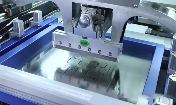
2.Stencil Preparation
During Printed Circuit Board (PCB) assembly, the process of printing solder paste onto the board is a common technique used to facilitate the placement of Surface Mount Components (SMC) accurately. To achieve accuracy, a stencil is typically used to create a fixed position for the components. The design of this stencil is based on the predetermined placement locations of the solder pads on the PCB, and is critical for ensuring that the SMC components are placed with the required precision.
The stencil’s manufacturing process typically involves creating openings at the predetermined solder pad locations to allow for the application of solder paste. This enables the accurate placement of the SMC components and ensures that the final product adheres to the required industry standards. Effectively, the quality and reliability of the PCB assembly process are directly linked to the accuracy of the stencil and its ability to create consistent component placement during the solder paste printing process.
3.Solder Paste Printing
In the field of electronic manufacturing, the process of connecting Surface Mount Components (SMC) with Printed Circuit Boards (PCB) typically involves the use of solder paste. This paste is composed of flux and tin, and is applied onto the solder pads located on the PCB using a stencil and a squeegee at an angle that typically ranges from 45 degrees to 60 degrees.
The purpose of the solder paste is to enable the formation of a strong and reliable connection between the SMC and the PCB. This connection is achieved through the process of reflow, which involves heating the solder paste to a specific temperature to enable the formation of a solid joint between the SMC and the PCB. By utilizing the stencil to apply the solder paste at a precise angle, the overall accuracy and consistency of the final product can be optimized, and any potential defects can be minimized.
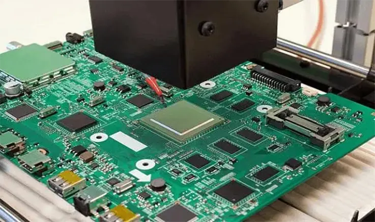
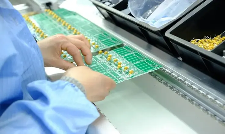
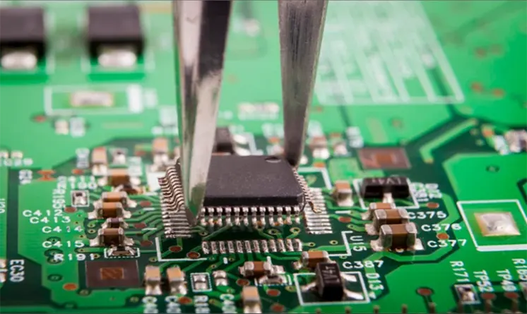
4.SMC Placement
In the electronic manufacturing industry, Printed Circuit Boards (PCBs) undergo a series of processes to achieve accurate and reliable assembly. One such process is achieved through the use of pick-and-place machines. These machines are responsible for placing the PCBs on a conveyor belt, where they are then transported to the component placement area, where electronic components are attached to the PCBs.
The pick-and-place machines play a crucial role in ensuring that the SMC components are positioned precisely on the PCB, in accordance with the predetermined solder pad placements created during the stencil printing process. The accurate placement of these components is essential to ensure a reliable and efficient operation of the final product.
5.Reflow Soldering
In electronic manufacturing, reflow soldering ovens are commonly used to bond electronic components to Printed Circuit Boards (PCBs). The process involves gradually raising the temperature of the PCB and components in a series of carefully controlled stages.
● The first stage of the process takes place in the pre-heat zone of the oven. The temperature of the PCB and components is gradually and concurrently raised, with a temperature increase rate of between 1.0 and 2.0 degrees Celsius per second. This stage continues until the temperature reaches between 140 and 160 degrees Celsius.
● The next stage is the soak zone, where the boards are held at a constant temperature between 140 and 160 degrees Celsius for a duration of between sixty to ninety seconds. This stage is crucial to ensure that the temperature of the PCB and components is stabilized and that the solder paste is evenly distributed.
● The reflow zone is the next stage, where the temperature rises at a rate of 1.0 to 2.0 degrees Celsius per second, reaching a peak temperature of between 210 and 230 degrees Celsius. This temperature is required to melt the tin contained in the solder paste, bonding the component leads to the pads on the PCB. The surface tension of the molten solder assists in holding the components in their proper positions.
● Finally, the boards move through the cooling zone of the oven, which is designed to allow the solder to freeze and solidify before they leave the heating zone to prevent joint fault. This controlled cooling process is necessary to ensure that the solder bonds are stable and reliable. Overall, the reflow soldering oven is a critical part of the electronic manufacturing process for creating reliable and high-quality electronic products.
When dealing with electronic circuit boards that require double-sided assembly, it is possible to carry out a repetitive process involving the printing, placement, and reflowing of the components. This can be accomplished via the use of either solder paste or adhesive material, both of which can effectively secure the components in their designated positions. It is an industry-standard practice to apply these techniques with precision and attention to detail, ensuring that the final product meets the necessary quality standards.
6. Clean & Inspection
Upon completion of the soldering process, it is crucial to perform a thorough cleaning of the circuit boards and conduct a meticulous examination to detect any possible defects. If defects are found, rework or repair procedures are necessary before the products can be stored. Various types of equipment are commonly employed in surface mount technology (SMT), including magnifying lenses, automated optical inspection (AOI) systems, flying probe testers, X-ray machines, and other similar devices, to facilitate the inspection and evaluation of the final products.
Benefits of Using a Third-party PCB manufacturer: JarnisTech
As a electronic and electrical manufacturer, it is evident that the development of a highly automated Surface Mount Technology (SMT) construction process can offer significant fabrication advantages. However, investing in the expensive production equipment required to accomplish this task can be challenging for many businesses specializing in SMT PCB design.
Fortunately, JarnisTech provides a viable and cost-effective solution for customized PCB fabrication, leveraging our specialized resources and streamlined processes to meet our clients’ unique specifications. Our company, as one of the foremost PCB manufacturers in China, places a strong emphasis on providing exceptional customer service and reliability. With a broad range of services available, we are well-equipped to assist businesses in incorporating high-quality SMT technology into their PCB fabrication process.
Factors to Consider When Selecting Right Technology for Your Design.
The selection of appropriate technology plays a pivotal role in achieving optimal design outcomes. For instance, during the schematic design process, the component selection stage presents an ideal opportunity to decide whether to utilize surface mount technology or through hole technology. By incorporating these components early on, there is a greater chance that the PCB layout will be constructed using the right component package tracks and footprints. Nonetheless, to make informed decisions about the technology that best suits your design requirements, you need to consider the following factors:
● Rework: When it comes to the prototyping stage, do you anticipate a significant amount of circuit rework?
● Use: How will the individual components be exposed to physical contact and other forms of stress? It is important to consider the frequency of contact and whether there will be additional stresses placed on the components.
● Price:Can a cost reduction be achieved by selecting a packaging style over another? An analysis should be conducted to determine the feasibility of cost savings through the selection of a specific packaging style.
● Power:You must consider how much heat and power the component will conduct while in use.
● Availability: In the process of developing your prototype, select the package that can most easily be accessible and use the appropriate gauge.
● Performance:What type of packaging approach provides the optimal opportunity to fully realize the potential of your circuit? It is essential to determine which packaging approach will offer the greatest potential for showcasing the capabilities of your circuit.
● Assembly: Determine which package style will provide you with high-quality assembly at the lowest possible cost.
Surface-mount technology (SMT) components may potentially provide the best solution for your design needs. However, it is important to address any concerns regarding through-hole components, especially if they are required. Your PCB manufacturer can be a valuable resource in assisting you in choosing the optimum path forward. With their extensive knowledge and experience working with various component package styles relevant to printed circuit boards, they can provide valuable insights and recommendations.
At JarnisTech, we have over 20 years of experience in assembling and fabricating PCBs, and our team of professional engineers has expert knowledge of components to guide you in the right direction. They can assist with identifying part availability and associated prices. At the same time, our engineers dedicated to the PCB manufacturing process will expertly develop your board with quality based on the design criteria.
Why Used Surface Mount Technology (SMT) For PCB Assembly
It is important to recognize the benefits of the Surface Mount Technology (SMT) assembly process in modern electronics manufacturing. With SMT, a wide range of components required for modern devices can be securely fastened to the surface of the printed circuit board in increasingly smaller footprints.
SMT assembly is highly adaptable to meet specific customer requirements while also providing a highly automated solution for large volume circuit board production. For designers in need of precise and efficient assembly to meet unique specifications, surface mount technology (SMT) is often the optimal choice.
For many years, JarnisTech has been a trusted provider of surface mount PCB assembly services to customers across diverse markets. With considerable expertise in contract manufacturing, we possess a wealth of knowledge in electronic component fabrication for a wide range of industries. Our company offers end-to-end solutions such as product prototyping, testing, contract manufacturing and more, thanks to our advanced equipment and skilled personnel. For any inquiries or to obtain a price estimate, please do not hesitate to contact our office
How Might SMT Assembly Lower Production Costs?
As an electronic manufacturer, it is important to recognize the cost-saving benefits associated with Surface Mount Technology (SMT). While initial machinery costs may be a consideration, the advantages of reduced manual labor are significant and two-fold.
Firstly, SMT offers long-term cost reduction benefits by decreasing the overall cost of labor while simultaneously improving production efficiency, ultimately resulting in cost savings. The use of software to simulate the assembly process prior to actual production significantly reduces the risk of errors during manufacturing, further contributing to cost savings. In addition, SMT assembly also has the potential to eliminate delays during production, which could otherwise result in additional expenses if not avoided.
In conclusion, SMT is a cost-efficient option for electronic manufacturers, and it offers precise and efficient assembly to reduce labor costs and improve productivity, resulting in long-term cost savings.
Through-hole Vs. Surface Mount Technology
As a PCB designer, it is important to understand both the through-hole installation and surface-mount technology (SMT) processes for soldering parts onto PCB boards. Through-hole installation involves inserting component leads into drilled holes on a bare PCB and soldering them on the other side of the board. While this is a standard method, SMT offers several benefits over through-hole installation, including easier automation, faster component placement, and improved high-frequency performance.
● However, it is worth noting that SMT is not appropriate for some components, such as power semiconductors with heat sinks and large transformers. The reason for this is that SMT components are only fastened by solder on the surface of the board and are not suitable for use in severe environments.
● In scenarios where component leads travel through the board, through-hole soldering may be a better option than other methods because it allows components to withstand greater environmental stress. Through-hole technology is still preferred in military and aerospace industries, which are frequently exposed to harsh environmental conditions. Additionally, through-hole technology is helpful for test and prototype applications that require manual adjustments and replacements, as it provides easy access to internal components.
In conclusion, while SMT is advantageous in several ways, through-hole technology still has its place in certain applications. As such, PCB designers must consider the specific needs of each project and carefully weigh the benefits and drawbacks of both installation options to determine the optimal solution.
Surface Mount Technology vs. Chip Scale Packaging
Surface Mount Technology (SMT) and Chip Scale Packaging (CSP) are two different methods of mounting electronic components on a printed circuit board. Despite some similarities, such as the use of solder paste and the absence of leads, there are a few differences between SMT and CSP.
● One key difference is the size of the components used. While SMT components typically range in size from 0201 to 1206, CSP components are much smaller, with a maximum size of about 2 mm. This makes CSP ideal for miniaturized devices.
● CSP also requires a higher degree of precision during assembly, with a smaller margin of error compared to SMT. CSP component placement and soldering need to be highly accurate and precise to avoid damaging the component and ensure proper connectivity.
● Another difference between SMT and CSP lies in their reliability. CSP components can be more prone to failure than SMT components due to their smaller size and greater sensitivity to environmental factors.
SMT and CSP have their respective advantages and challenges. SMT is suitable for larger, more complex devices, whereas CSP is excellent for miniaturized electronic devices that require high-density packaging in a small space.
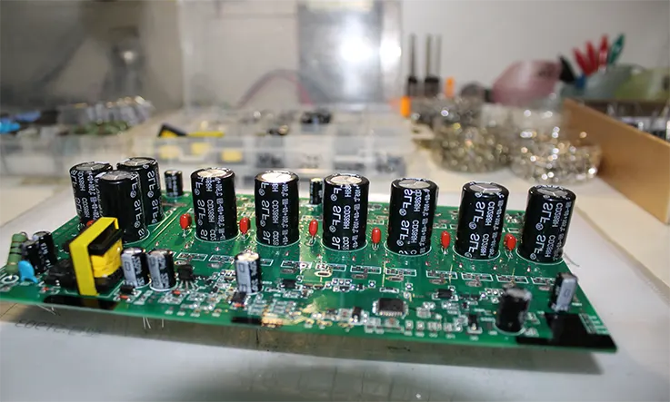
Components Types of Surface Mount Technology (SMT)
● Passive Components: Resistors and capacitors are regarded as staple components in the field of electronics. It is worth noting that some versions of these components are also equipped with coils that provide the necessary ability to handle high levels of electrical current. Such components are frequently utilized in electronic devices that exhibit a notable power consumption.
● Transistors and Diodes: The size of these components is very small, and they are designed to occupy a minimal amount of space. Additionally, transistors feature three legs which make them easier to handle and join through the process of soldering.
● Integrated Circuits: Integrated circuits come in a range of configurations, with varying numbers of pins. The number of pins can be as low as eight or as high as two hundred and fifty, particularly in circuits that contain microprocessors. The use of surface-mount technology (SMT) has facilitated smaller ICs without sacrificing functionality or performance, allowing for the retention of all the expected features and capabilities.
Future Trends in Surface Mount Technology
Surface Mount Technology (SMT) has undergone significant advancements over the years and is expected to continue evolving in the future. Some potential trends that may shape the future of SMT include:
● Miniaturization: With the growing demand for smaller and more powerful electronic devices, the trend towards miniaturization in SMT is likely to accelerate. SMT components are already incredibly small, but new innovations such as 3D printing and advanced materials may enable even smaller components in the future.
● Increased Integration: Another trend is towards the integration of multiple functions into a single component. This is already being seen with System-in-Package (SiP) technology, which integrates multiple components into a single module. In the future, we may see further developments that allow for even more integration of components.
● Advanced Materials: Advanced materials, such as flexible or stretchable substrates, may become more prevalent in SMT. These substrates could enable the development of devices that can bend, twist, or stretch, leading to new applications and use cases.
● Automated Inspection and Assembly: With the increasing complexity and miniaturization of SMT components, automated inspection and assembly technologies will become more critical. This may include advancements in quality control, such as AI-based inspection systems or more advanced machine learning algorithms.
● IoT and Smart Manufacturing: The future of SMT is also closely tied to the development of the Internet of Things (IoT) and smart manufacturing. These technologies will enable more efficient and automated production techniques and could lead to the creation of truly intelligent factories.
Therefore, the future of SMT is likely to be shaped by advances in miniaturization, integration, materials, automation, and smart manufacturing technologies.
To Conclude
The gradual shift from the conventional through-hole method to surface mount technology is apparent, and the latter holds a significant position in the current industry. The adoption of surface mount technology in the printed circuit board (PCB) manufacturing industry has led to a reduction in manufacturing durations for electronic goods and devices, resulting in noteworthy advancements. Consequently, the widespread incorporation of this technology is propelling the PCB manufacturing industry towards a promising future.
Related Posts:
1. What Is PCB Etching and How to Make a perfect PCB Etching?
2. The Best PCB Panelization Guide
3. The Importance of 3D Printed PCBs in Modern Electronics Production
4. Understanding PCB Delamination: A Comprehensive Guide
5. The Best Backplane Printed Circuit Boards Factory
6. An Overview of Through-hole Technology (THT)