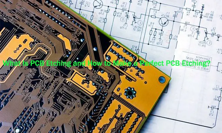
Printed Circuit Boards (PCBs) are the backbone of most electronic devices. They provide a physical base for mounting and interconnecting components, and they play a crucial role in the operation of electronics. The process to manufacture a PCB involves various steps, one of the most vital of which is the etching process.
Printed circuit boards (PCBs) play a pivotal role in the electronics industry, offering both widespread usage and cost-effectiveness. They enable the assembly of intricate circuits within confined spaces, effectively minimizing the risk of loose connections. In industrial settings involved in PCB manufacturing, various methods and specialized machinery are employed. However, it is also possible to carry out PCB etching at home with relative ease. This article provides valuable insights into the realm of DIY PCB etching and factory PCB etching, encompassing essential steps, required tools, and safety precautions, among other pertinent aspects.
What is PCB Etching?
PCB etching is the process of removing unwanted copper from the board to create a planned circuit layout. This process is integral to circuit board manufacturing as it shapes the pathways for electricity to travel throughout the board.
Furthermore, the etching process employed by industrial circuit board fabricators can be divided into two distinct methods: acidic etching and alkaline etching.
Acidic Etching
Acidic etching is specifically employed in the elimination of copper from internal layers in standard rigid FR-4 circuit boards. This choice is attributed to its capacity for precise and less aggressive action. The acidic process exhibits compatibility with the photoresist material and results in minimal undercutting during the metal etching process. Nonetheless, it is important to acknowledge that acidic etching entails a longer duration compared to alternative methods, thus necessitating a trade-off in terms of time efficiency.
Alkaline Etching
Alkaline etching is employed for the outer layers of circuit boards, as it offers a faster process that helps maintain the uniformity of the remaining copper. Alkaline etching, being more active than acidic etching, necessitates meticulous monitoring to ensure precise execution.
The utilization of both acidic and alkaline etching processes is advantageous due to their high etching rates, cost-effectiveness, and ability to effectively etch various metal materials. PCB fabricators must diligently uphold their etching procedures to mitigate exposure to hazardous liquids and fumes, as well as prevent any potential water contamination. Now, let us delve into the application of this etching technique in the fabrication of printed circuit boards.
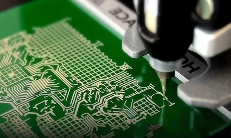
The Etching Process of PCB Factory
The etching process can be broken down into four main steps:
1. Laminating: The process begins with a substrate (usually fiberglass) covered with a thin layer of copper. This copper is laminated with a resist layer, which is a type of material that’s resistant to the etching solution. This layer is typically photoresist, which is sensitive to light.
2. Exposing: The board, covered in resist, is then exposed to ultraviolet light. A mask, also known as a stencil or photomask, is used to cover the areas of the board that should remain copper. The UV light hardens the exposed photoresist.
3. Developing: After exposure, the board is bathed in a developing solution. This solution removes the unhardened photoresist from the areas not exposed to the UV light, revealing the copper underneath.
4. Etching: The board is then submerged in an etchant solution, often ferric chloride or ammonium persulfate, which dissolves the exposed copper. The hardened photoresist protects the copper beneath from the etchant, and thus the desired circuit pattern is left on the board.
5. Stripping: Finally, the remaining photoresist is stripped away, leaving a clean, etched board ready for the next stages of PCB production.
Importance of PCB Etching
Etching is crucial as it shapes the pathways that allow electricity to flow between different components on the PCB. It ensures that the circuits are accurate and precise, which is vital for the reliable operation of the final electronic product.
Without the etching process, it would be impossible to create the complex, multi-layered circuit designs that are typical in modern electronics. It is a cost-effective method that enables mass production of high-quality, consistent PCBs.
DIY:Materials and Necessary Tools
The subsequent list encompasses key tools and materials that are essential for undertaking the process of DIY PCB etching.
♦ Laser Printer
♦ Cloth Iron
♦ Drill machine
♦ Soldering iron
♦ Steel wool or Sandpaper
♦ Gloves
♦ Photo paper / Glossy paper
♦ Permanent marker (preferably black)
♦ Ferric Chloride, also known as the Etching solution
Prior to delving into the step-by-step process of PCB etching at home, it is crucial to emphasize the indispensability of the aforementioned materials and equipment. Their availability is paramount to ensure the successful execution of the PCB etching procedure.
For instance, the absence of rubber gloves can lead to discomfort and potential harm to your hands. Similarly, the lack of steel wool or sandpaper will impede the effective removal of the top oxide layer from the copper material and hinder proper adhesion of the image from the paper onto the photoresist layer of the PCB. Smooth and sanded surfaces facilitate the precise transfer of the image onto the PCB.
Consequently, it becomes evident that the possession of the appropriate tools and materials is imperative to achieve satisfactory results during the PCB etching process. The absence of even a single item from the required list can detrimentally impact the overall experience and outcome of the PCB etching endeavor.
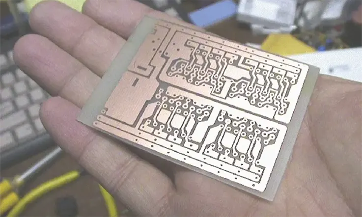
Steps to DIY PCB Etching
The process of DIY PCB etching involves the following steps:
1. Design and Prepare the PCB Layout: Use PCB design software to create the desired layout of your circuit. Ensure accurate placement of components and trace connections. Once the design is ready, print it on a suitable medium, such as a transparency film or specialized PCB transfer paper.
2. Prepare the Copper Clad Board: Cut a piece of copper clad board to the desired size for your PCB. Clean the board’s surface using steel wool or fine-grit sandpaper to remove any oxidation or impurities. Ensure that the board is free from dust and debris.
3. Transfer the PCB Layout: Place the printed layout onto the copper side of the board, aligning it correctly. Apply heat and pressure using a laminator or a heated iron to transfer the toner or ink from the printed layout onto the board’s surface. Allow the board to cool before proceeding.
4. Etch the PCB: Prepare an etching solution, typically a mixture of ferric chloride or ammonium persulfate and water, following the manufacturer’s instructions. Wear protective gloves and goggles. Immerse the board into the etching solution and agitate it gently. Monitor the etching progress until all unwanted copper is dissolved, leaving only the desired circuit traces.
5. Rinse and Clean the PCB: Remove the board from the etching solution and rinse it thoroughly with water to halt the etching process. Use a scrub brush or sponge to remove any remaining toner or ink. Dry the board completely.
6. Remove the Toner or Ink: To remove the toner or ink from the PCB surface, soak it in an appropriate solvent, such as acetone or lacquer thinner. Gently scrub the board with a brush to remove the remaining toner or ink, revealing the copper traces.
7. Inspect and Test the PCB: Carefully inspect the PCB for any defects or incomplete traces. Use a multimeter or continuity tester to verify the connectivity of the circuit. Make any necessary repairs or modifications if needed.
8. Apply Solder Mask and Silkscreen (optional): If desired, apply a solder mask to protect the copper traces and create a professional appearance. Additionally, you can add a silkscreen layer for labeling components or adding design elements.
It is important to note that DIY PCB etching requires proper safety precautions and adherence to guidelines. Follow all safety measures, such as working in a well-ventilated area, wearing protective gear, and disposing of chemicals appropriately.
Safety Measures While Undertaking PCB Etching
When undertaking PCB etching, it is crucial to prioritize safety and take appropriate measures to mitigate potential risks. The following guidelines should be adhered to:
1. Personal Protective Equipment (PPE): Always wear the necessary PPE, including safety goggles or glasses to protect your eyes from chemical splashes or flying debris. Gloves and an apron should be worn to shield your skin from corrosive chemicals.
2. Well-Equipped Workspace: Set up your workspace in a well-ventilated area to minimize exposure to hazardous fumes. Ensure that you have access to an eyewash station, a telephone for emergencies, and a fully stocked first aid kit nearby.
3. Proper Handling of Chemicals: Familiarize yourself with the properties and potential hazards of the chemicals used in the etching process. Follow the manufacturer’s instructions for storage, handling, and disposal of chemicals. Avoid contact with skin and eyes and work with chemicals in a controlled manner.
4. Power Tool Safety: If power tools are involved, such as drills or routers, exercise caution when operating them. Follow proper safety procedures, including wearing appropriate protective gear and ensuring the workspace is clear of any potential hazards.
5. Adequate Ventilation: Maintain good ventilation in the workspace to minimize the buildup of harmful chemical vapors. If necessary, use exhaust fans or work in a fume hood to remove fumes effectively.
6. Emergency Preparedness: Have a clear understanding of emergency procedures and escape routes in case of accidents or chemical spills. Keep emergency contact numbers readily available and ensure you know how to use the eyewash station and first aid supplies.
7. Seek Expert Guidance: If you are unsure about any aspect of the PCB etching process, consult with an experienced professional or seek guidance from knowledgeable resources. It is better to ask for assistance than to proceed with uncertainty.
By following these safety measures, you can reduce the risk of accidents, injuries, and chemical exposure during PCB etching, ensuring a safer working environment.
Why Choose JarnisTech for Your PCB Etching Solutions?
We understand your interest in engaging in the process of DIY PCB etching. It can be an enjoyable and educational experience, allowing you to acquire new skills. However, we also recognize that this endeavor can present challenges along the way.
At Jarnistech, we aim to provide comprehensive PCB etching solutions that set us apart from numerous other companies in the industry. Our commitment to delivering exceptional quality PCBs is matched by our dedication to providing outstanding customer care and efficient service.
By choosing us, you can benefit from several key advantages. Firstly, we prioritize saving our customers’ valuable time and hard-earned money. Through our streamlined processes and prompt delivery, we ensure a swift turnaround time without compromising on the quality of our products. Additionally, we strive to offer competitive quotes that are difficult to resist, providing our customers with cost-effective solutions.
Our overarching objective is to instill peace of mind in our valued clients. This commitment is evident throughout every aspect of our operations, from the quality of our PCBs to our customer-centric approach. We are dedicated to meeting and exceeding customer expectations, ensuring a positive experience throughout the entire engagement.
In summary, when choosing Jarnistech for your PCB etching needs, you can expect exceptional customer service, high-quality products, efficient delivery, and competitive pricing. We look forward to the opportunity to serve you and contribute to the success of your PCB projects.
Conclusion
PCB etching is a crucial step in the production of circuit boards. It is a process that requires precision and accuracy to ensure the final product functions as intended. As electronics continue to miniaturize and grow more complex, the etching process will continue to be a key part of circuit board manufacturing.
Related Posts:
2. The Best PCB Panelization Guide
3. The Importance of 3D Printed PCBs in Modern Electronics Production
4. Understanding PCB Delamination: A Comprehensive Guide
5. The Best Backplane Printed Circuit Boards Factory
6. An Overview of Through-hole Technology (THT)
7. Detail Talk Surface Mount Technology