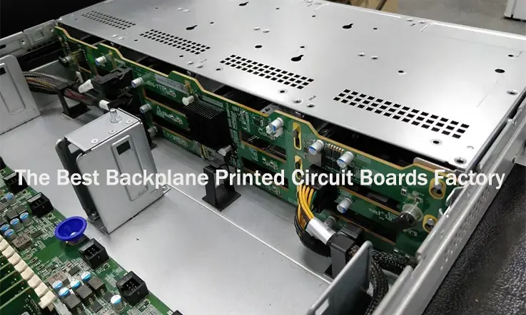
Backplane PCBs are crucial connector printed circuit boards used in various applications, projects, and products, making them increasingly valuable in modern times. They offer greater functionality and benefits for PCB fabrication.
JarnisTech is a leading manufacturer that specializes in backplane PCBs. Given the significant importance of these PCBs in fabrication, JarnisTech employs a meticulous manufacturing process and utilizes state-of-the-art technologies.
Whether you seek specific information about this particular type of printed circuit board or are interested in gaining insights into our backplane PCB facilities, this comprehensive guide will provide you with all the necessary details. It covers a wide range of topics related to backplane PCBs, ensuring you are well-informed about their capabilities and advancements.
What is a Backplane PCB ?
A backplane PCB serves as a vital component in electronic systems as it facilitates the interconnection of multiple devices. Acting as the central interface, it forms the backbone that enables seamless communication and data transfer among various subsystems and components.
Essentially, a backplane PCB comprises an array of connectors, slots, and sockets that facilitate the insertion of diverse modules or daughter cards. These modules encompass a wide range of devices, such as CPUs, memory modules, input/output cards, and more. Through the backplane, these modules establish power and data connections, fostering efficient communication and data exchange among them.
Design Considerations for Backplane PCBs
Designing a backplane PCB involves several considerations to ensure its optimal performance. Some of the key design considerations for backplane PCBs are:
Layer count: The number of layers required for a backplane PCB depends on the complexity of the system and the number of signals to be routed. A higher number of layers can provide better signal integrity, but also increase the cost and complexity of fabrication.
Trace width and spacing: The trace width and spacing must be carefully designed to ensure that the backplane can handle the required current and provide a low impedance path for signals. The trace width and spacing must be optimized for the specific signal frequency, skew, and crosstalk requirements.
Materials selection: Backplane PCBs are typically made using high-performance materials that provide good electrical properties, such as FR-4, polyimide, and Rogers materials. The selection of materials depends on the specific requirements of the system, such as thermal management, mechanical strength, and electrical performance.
Thermal management: Backplane PCBs can generate a significant amount of heat, especially in high-performance systems. Adequate thermal management must be incorporated into the design to ensure that the backplane can operate within the required temperature range. This can include the use of thermal vias, embedded heat sinks, and proper component placement.
Signal integrity: Backplane PCBs must maintain signal integrity to ensure reliable communication between components. This requires careful consideration of trace length, impedance matching, and termination techniques.
Electrical performance: Backplane PCBs must meet the electrical performance requirements of the system, such as voltage, current, and power requirements. This requires careful consideration of the design parameters and simulation of the electrical performance using software tools.
EMI/EMC: Backplane PCBs must also consider electromagnetic interference (EMI) and electromagnetic compatibility (EMC) requirements to avoid interference with other components and systems. This requires careful shielding and grounding techniques, as well as compliance with regulatory standards.
Overall, the design of a backplane PCB requires careful consideration of multiple factors to ensure optimal performance and reliability.
Types of Backplane PCB
Backplane PCBs incorporate printed circuit boards featuring expansion slots or sockets to facilitate interconnection with other printed circuit boards. There exist two primary types of backplane PCBs: active backplanes and passive backplanes. Both variants effectively cater to industrial requirements.
Active Backplane PCB
An active backplane PCB incorporates motherboard circuitry and bus control for facilitating communication among its slots. It features the necessary slots and circuitry to maintain efficient data exchange on the board. Notably, an active backplane does not include processor complex components such as the central processing unit (CPU), cache, or chipset.
Passive Backplane PCB
A passive backplane PCB is equipped with circuitry designed for bus connections. It may incorporate drivers and buses depending on specific requirements. Essentially, a passive backplane primarily consists of bus connectors with minimal or no additional circuitry. The communication between boards is managed by expansion boards connected to the passive backplane. A passive backplane PCB can accommodate one or more expansion boards. In industrial settings, passive backplanes often feature bridges that establish connections between two buses, which can be of the same or different types.
How Does A Backplane PCB Work ?
A Backplane PCB functions as a collection of electric connectors arranged in a parallel configuration. Each pin of every connector is connected to a common pin, effectively establishing connectivity across all pins.
Primarily, a Backplane PCB serves as a specialized form of PCB that provides structural support for connecting additional printed circuit boards. It enhances stability and mechanical strength in the PCB assembly.
Moreover, it serves as a platform for integrating daughterboards, which are additional components of the system.
Various daughterboards fulfill distinct functions within the PCB system. Backplane PCBs are highly versatile and widely employed, primarily due to their ability to facilitate the easy interchangeability of different cards.
Notably, backplane PCBs offer modularity, scalability, and other advantages that contribute to their suitability for diverse applications. When an external server signal enters the system, it passes through a daughter card and subsequently reaches the backplane PCB, which regulates the signal according to the required output.
Backplane Manufacturing Difficulties
Backplane manufacturing difficulties can arise due to various reasons. Backplanes are an essential component of electronic systems that provide a communication channel between different modules and components. These difficulties can arise during the design, fabrication, assembly, or testing stages. Some of the common backplane manufacturing difficulties are:
Signal Integrity Issues
One of the major difficulties in backplane manufacturing is ensuring signal integrity. Signal integrity issues can arise due to crosstalk, electromagnetic interference (EMI), and signal attenuation. These issues can result in signal distortion, data errors, and system failures.
Fabrication Issues
Backplane fabrication involves complex processes such as drilling, plating, and laminating. Any errors or defects during the fabrication process can result in signal loss, short-circuits, or open-circuits. Fabrication issues can also arise due to poor quality control, lack of precision, or improper tooling.
PCB Thickness: The increased thickness of Backplane PCBs is a result of incorporating numerous high-speed controlled impedance transmission lines, supply rail planes, and return paths. When transmitting high-frequency data over extended traces, wider signal traces are necessary to mitigate signal attenuations. To maintain impedance and minimize signal absorption, a thicker dielectric is required. However, augmenting trace width reduces signal density in a given layer’s unit area, while increasing the dielectric thickness contributes to an overall increase in PCB thickness.
As the number of signal layers, power planes, and return planes increases in pursuit of optimal performance, the layer count of the PCB can reach 20 or more. This presents a challenge for manufacturers in maintaining standard PCB thickness given the available materials and impedance matching parameters.
For backplanes up to a thickness of 5 to 6mm, high-speed fine PCB drilling for vias and connectors functions adequately. However, thicker PCBs necessitate larger drill diameters. Manufacturers are constrained by higher drill aspect ratios, such as 8:1, which can impede volumetric production. As a result, thicker PCBs require multiple drill passes for a single via.
PCB Pressing: In the manufacturing process of thicker backplanes, the complexity of drilling increases. Lengthy drill holes necessitate multiple drilling operations, resulting in reduced drilling accuracy and a decrease in PCB yield percentage. Moreover, the high frequency performance of the backplanes is compromised as a consequence.
High density etching: In a backplane PCB, the extensive number of connectors results in a substantial utilization of PCB real estate for mounting holes and pads. PCB designers face the challenge of increasing the density of signal routing while adhering to impedance and trace length requirements, instead of simply adding more layers to the PCB. This heightened signal density brings about increased complexity during etching, pushing the geometries of traces, via-holes, pad-holes, and annular rings towards the limits of fabrication tolerances.
Impedance matching: Achieving impedance matched PCB fabrication poses challenges when dealing with high-speed data transmissions on backplanes. It is generally not advisable to transmit data in the gigabits-per-second range over standard FR-4 materials. The selection of materials for backplane PCBs is influenced by factors such as dielectric constant and dissipation factor. This presents a challenge for PCB manufacturers, as they need to provide PCBs using the required materials. Additionally, ensuring transmission line impedance, via impedance, and connector pad-to-pin impedance further adds to the complexity. Introducing a new material type necessitates slight adjustments to the PCB manufacturing process at the manufacturer’s facility.
Via back-drilling: Unused copper sections in a PCB can introduce stub effects in high-frequency signals. Similarly, the presence of unused via barrel copper and annular rings can also cause stub effects. As a result, PCB manufacturers are compelled to employ back-drilling techniques. This involves removing the excessive via barrel copper from through-hole vias in a fabricated PCB. The manufacturer accomplishes this by re-drilling the designated holes with a different drill size, leaving a specific length of via copper after the final layer connection. However, this process slows down production and can lead to inaccuracies in PCBs.
Connectors Alignment: High-speed backplanes are equipped with well-matched impedance connectors. Typically, a backplane contains approximately 50 impedance controlled differential pairs per square inch, resulting in a substantial quantity of differential pairs, around 500 pairs within a plane. The utilization of high-density SMD and through-hole connectors allows for smaller PCB sizes; however, it necessitates frequent blind press-fit insertion and extraction of daughter cards. This process poses durability challenges for the PCB. Manufacturers face the constraint of preserving the hole locations and connector geometry, while also ensuring consistent signal integrity throughout the entire PCB.
Layer registration: In high-speed, high-density PCBs, layer registration can lead to reduced accuracy during processes such as copper etching, lamination, drilling, and overall dimensional stability. This poses challenges for manufacturers in terms of maintaining signal integrity and achieving a high PCB yield, particularly when dealing with smaller sizes.
Aspect Ratio: The aspect ratio refers to the ratio between the drill size and the thickness of a PCB. When dealing with backplanes that have dense signal routing, higher copper layer counts, and a large number of vias and connector through-holes, the aspect ratio tends to be high, which presents manufacturing challenges. PCB design engineers aim to establish an appropriate aspect ratio that ensures efficient PCB assembly in China and durability. Manufacturers are under pressure to produce PCBs with a 10:1 aspect ratio, although a more commonly used figure is 6:1.
Assembly Difficulties
Backplane assembly involves connecting different modules and components to the backplane. Assembly difficulties can arise due to component misalignment, poor soldering, or incorrect routing. These issues can result in signal loss, data errors, or system failure.
Testing Challenges
Backplane testing is essential to ensure proper functionality and signal integrity. Testing difficulties can arise due to the complexity of the backplane and the need for specialized equipment and testing procedures. Testing challenges can also arise due to the high-speed and high-frequency signals that are transmitted through the backplane.
To overcome these difficulties, backplane manufacturers need to have a robust quality control system, proper design guidelines, and specialized equipment for fabrication and testing. They also need to have skilled personnel with expertise in backplane manufacturing and testing. Additionally, implementing advanced technologies such as simulation and modeling can help in identifying and addressing backplane manufacturing difficulties.
Technologies of Backplane PCB in Manufacturing
The manufacturing of backplanes requires special attention and advanced technologies due to their heightened complexity and specific requirements.
Reflow Soldering
Due to the increased thickness and weight of backplane boards, heat dissipation becomes more challenging during reflow soldering. It takes longer for backplanes to cool down after the soldering process. Therefore, it is essential to reinforce the reflow soldering oven to allow for an extended cooling time for backplane boards. Additionally, the use of forced air cooling at the exit of the reflow soldering oven helps facilitate the cooling of backplane boards.
Cleaning
Backplanes, with their greater thickness and larger number of drilling holes or vias, are more prone to the flow of working fluid during the manufacturing process. Thorough cleaning of the drilling holes using high-pressure cleaning machines is crucial to prevent the retention of working fluid within these holes or vias.
Layer Alignment
With higher layer counts and drilling hole numbers, achieving precise layer alignment becomes exceedingly difficult. Therefore, meticulous attention and advanced technologies must be employed during the fabrication process of backplane boards to ensure accurate layer alignment.
Component Assembly
Traditionally, backplanes primarily featured passive components to ensure reliability. However, there has been an increasing trend of integrating active components, such as BGAs (Ball Grid Arrays), on backplanes to maintain cost-effectiveness in active board designs. Component assemblers need to possess the capability to handle smaller capacitors, resistors, and silicon-packaged components. Additionally, the larger size of backplanes necessitates the use of larger assembly platforms.
Advantage of Using a Backplane PCB
Utilizing a backplane PCB offers notable advantages by simplifying the assembly of intricate electronic systems through efficient interconnection of multiple components. The following are key benefits associated with the use of backplane PCBs:
Streamlined Interconnectivity: Backplane PCBs enable straightforward interconnectivity among various circuit boards or modules. Acting as a central backbone, they eliminate the need for multiple connectors and cables, thereby simplifying assembly processes, lowering the risk of signal loss, and enhancing overall system reliability.
Scalability: Backplane PCBs are designed to accommodate multiple slots or connectors, ensuring easy integration of new components or system expansion without substantial modifications. This scalability feature presents a cost-effective solution suitable for future system upgrades or expansions.
Enhanced Signal Integrity: Backplane PCBs offer a consistent and controlled signal transmission environment, minimizing signal distortion, crosstalk, and electromagnetic interference. This leads to improved system performance by preserving signal quality.
Space Efficiency: Implementing backplane PCBs conserves valuable space within electronic systems by reducing the requirement for cumbersome and intricate cabling. This proves particularly advantageous for systems with limited physical space or those requiring high portability.
Given these advantages, backplane PCBs find widespread application in computing systems such as servers, routers, and telecommunications equipment. They are also commonly used in industrial control systems, medical equipment, and other intricate electronic systems. The design and layout of a backplane PCB can vary, tailored to meet the specific requirements of the system.
Typically, they incorporate multiple layers of copper traces and vias to facilitate high-speed data transfer and efficient power distribution.
The Best Backplane PCB Manufacturer – JarnisTech
JarnisTech, a reputable Chinese manufacturer, specializes in the production of high-quality backplane PCBs. With two decade of experience in PCB manufacturing, we are committed to delivering authentic and reliable products. Our dedicated engineering team is readily available to meet your specific requirements. Our backplane PCBs are versatile, catering to a wide range of applications including electronic consumer goods, telecommunications, military, aerospace, and beyond. JarnisTech is your trusted and dependable business partner. We encourage you to submit your inquiries today for prompt assistance.
Related Posts:
1. What Is PCB Etching and How to Make a perfect PCB Etching?
2. The Best PCB Panelization Guide
3. The Importance of 3D Printed PCBs in Modern Electronics Production
4. Understanding PCB Delamination: A Comprehensive Guide
6. An Overview of Through-hole Technology (THT)
7. Detail Talk Surface Mount Technology