
Consumer electronics are increasingly becoming more compact and powerful. As the market demands smaller, smarter devices, Consumer PCB technology continues to evolve to meet these expectations. PCBs (Printed Circuit Boards) serve as the backbone of virtually all electronic devices today, from wearables and smartphones to IoT (Internet of Things) devices and automotive electronics.
The Consumer PCB industry plays a critical part in driving innovation, allowing for higher-density designs, improved functionality, and reduced device footprints. As the market for consumer electronics expands, manufacturers must understand the nuances of designing, sourcing, and producing these critical components to stay ahead of the competition.
Types of Consumer PCBs: The Backbone of Modern Electronics
When you’re getting into PCB design for consumer devices, it’s not just about slapping components on a board and calling it a day. Knowing your way around the types of Consumer PCBs helps you tailor each board for the job. Whether it’s a rigid, flexible, or high-frequency setup, choosing the right PCB type can make your device run smoother than a well-oiled machine. Let’s break down the basics and see which types fit different devices best.
Single-Sided PCBs:
These are your bread and butter when it comes to low-cost, simple consumer electronics. Single-sided PCBs feature all components mounted on one side of the board, making them easier to manufacture and cheaper. These are typically used in items where complex functions aren’t required—think of basic household electronics or older tech gadgets.
Example: Early remote controls, simple radios, and toys often used single-sided PCBs for their cost-effectiveness and simplicity.
Double-Sided PCBs:
Double-sided PCBs allow for components to be mounted on both sides of the board, effectively doubling the space for circuits. This is great for slightly more complex devices that still don’t need the added bulk of multilayer boards. These are commonly used in consumer products that need a bit more power or complexity.
Example: Home appliances like microwaves or low-end smart devices often use double-sided PCBs.
Multi-layer PCBs:
Now, when you’re talking about high-tech, multi-layer PCBs are your go-to. These boards have multiple layers of copper and insulating material, allowing for more circuits in a smaller space. These are used in high-performance devices like smartphones, tablets, and laptops where space and power are at a premium.
Example: Your high-end laptop or a smart TV remote will often contain a multi-layer PCB to keep everything compact and functional.
Rigid PCBs:
Rigid PCBs are the traditional type of PCB that uses a solid base material. These are commonly used in devices that don’t require bending or flexibility. They’re reliable, strong, and work well in a range of applications.
Example: Desktop computers, home entertainment systems, and kitchen appliances.
Flexible PCBs:
Flexible PCBs are designed to bend or fold without damaging the components. This allows them to fit into compact, flexible spaces—think of wearables, like fitness trackers or smartwatches, that need to be lightweight and flexible.
Example: Smartwatches, fitness trackers, and even some medical devices that need to fit snugly around the body.
Rigid-Flex PCBs:
Rigid-flex PCBs combine the best of both worlds: rigid boards that remain stationary and flexible parts that can bend and adjust. These are used in applications that require both durability and flexibility in the same device, perfect for wearables or cutting-edge mobile tech.
Example: Foldable smartphones or advanced camera systems often rely on rigid-flex PCBs for their compact, multifunctional design.
High-Frequency PCBs:
High-frequency PCBs are specifically engineered to handle signals at high frequencies—think wireless communication, like Wi-Fi or Bluetooth. These are built with materials that reduce signal loss and ensure faster, more reliable communication.
Example: Modern Wi-Fi routers or Bluetooth devices often rely on high-frequency PCBs to ensure stable signal transmission.
Aluminum-backed PCBs:
Aluminum-backed PCBs are primarily used in applications that require heat dissipation, such as power supply units or LED lighting. The aluminum base ensures that heat is efficiently drawn away from components, preventing overheating.
Example: For applications like LED lighting systems or automotive headlights, keeping the heat under control is a top priority to maintain steady performance over time. These setups need reliable heat dissipation solutions to avoid overheating, which could reduce the lifespan or efficiency of the lights. By incorporating materials and designs geared towards efficient thermal management, these systems stay cooler, keeping their performance on point for the long haul.
High-Speed PCBs:
High-speed PCBs are engineered for high data transmission speeds, often used in devices that require fast processing and real-time data exchange, like gaming consoles and high-performance computers.
Example: Graphics cards or advanced gaming peripherals use high-speed PCBs to keep up with the demand for rapid data transfer.
HDI PCBs:
HDI (High-Density Interconnect) PCBs are the heavy-hitters when you need ultra-compact designs with complex wiring. HDI PCBs pack a ton of circuits into a small space, which is why they’re used in high-end consumer tech like smartphones and tablets.
Example: Apple’s latest iPhones or top-of-the-line Android devices make use of HDI technology to keep everything compact, fast, and reliable.
LED PCBs:
LED PCBs are built to handle the unique needs of light-emitting diodes (LEDs), focusing on effective heat dissipation and stable power flow. This design is a perfect match for the expanding world of energy-saving lighting and high-resolution displays, where keeping LEDs cool directly impacts performance and lifespan. With reliable thermal management and consistent power, LED PCBs make sure those bright lights stay steady. This is especially useful for modern lighting setups where efficiency and durability matter most.
Example: LED bulbs, LED TVs, and digital billboards.
RF PCBs:
RF (Radio Frequency) PCBs are designed for handling high-frequency signals in the radio wave spectrum. These are commonly used in communications devices, such as cellular phones, radios, and wireless internet equipment.
Example: Radios, cell phones, and wireless communication devices all depend on RF PCBs to function.
Metal Core PCBs:
Metal core PCBs, often using materials like aluminum, are perfect for managing heat in high-power applications. These are commonly used in LED lighting, power supplies, and automotive electronics.
Example: High-powered LED arrays or power converters in electric vehicles use metal core PCBs to prevent overheating.
Gold Finger PCBs:
Gold finger PCBs are a specific type of PCB used to create a connection between different circuit boards. They are characterized by gold-plated connectors or fingers that enable high-quality electrical connections.
Example: Gold finger PCBs are typically found in memory cards or high-speed interconnects like PCIe cards.
Ceramic PCBs:
Ceramic PCBs are used in applications requiring high thermal stability and electrical insulation. These PCBs are often used in industrial and medical equipment where overheating is a concern.
Example: Medical devices and industrial sensors often use ceramic PCBs for their durability and heat resistance.
Table of Common PCB Types
| PCB Type | Features | Common Applications |
| Single-Sided PCBs | Simple, low-cost | Basic consumer electronics like radios, toys |
| Double-Sided PCBs | Components on both sides | Home appliances, simple smart devices |
| Multi-layer PCBs | Multiple conductive layers | Smartphones, tablets, high-performance computers |
| Rigid PCBs | Solid, durable, traditional design | Desktop computers, home entertainment systems |
| Flexible PCBs | Flexible, bendable | Wearables like fitness trackers and smartwatches |
| Rigid-Flex PCBs | Combines rigid and flexible sections | Foldable smartphones, advanced cameras |
| High-Frequency PCBs | Designed for high-speed signals | Wi-Fi routers, Bluetooth devices |
| Aluminum PCBs | Excellent heat dissipation | LED lighting, automotive headlights |
| High-Speed PCBs | Optimized for high data speeds | Gaming consoles, high-performance computers |
| HDI PCBs | Ultra-compact with complex wiring | Smartphones, tablets |
| LED PCBs | Designed for LED applications | LED lighting, digital billboards |
| RF PCBs | Handles radio frequency signals | Radios, cell phones, wireless communication devices |
| Metal Core PCBs | Metal-backed for heat dissipation | High-power LEDs, power supply units |
| Gold Finger PCBs | Gold-plated connectors | Memory cards, high-speed interconnects |
| Ceramic PCBs | High thermal and electrical stability | Medical devices, industrial sensors |
This table sums up the key features and applications of various types of Consumer PCBs. Depending on the product you are designing or manufacturing, you’ll need to select the most appropriate type to meet both technical requirements and cost considerations
Key Design Considerations for Consumer PCBs
Designing a Consumer PCB goes beyond just fitting components onto a board—it’s about crafting tailored solutions that address specific functionality while staying within tight design constraints. As consumer electronics become more advanced, the complexity of PCBs increases. Designing high-density boards that can fit multiple layers of circuits in small spaces is a must. This is especially important in consumer products like smartphones, wearables, and home appliances, where space is at a premium, but performance can’t be compromised.
High-Density Interconnects (HDI) for Advanced Consumer PCB Designs
High-Density Interconnects (HDI) in PCB design bring incredible versatility to consumer electronics, particularly compact gadgets like smartphones and wearables. HDI boards allow more complex circuitry to fit within limited spaces, enhancing functionality without added bulk. This technology supports slim profiles and efficient layouts, letting designers meet high performance demands for portable devices. So, whether it’s fitting more layers or refining interconnections, HDI is the go-to solution for maximizing device capability in minimal space.
HDI PCBs use smaller vias, high-density traces, and multiple layers to pack more functionality into a smaller area. Let’s break down some of the key attributes of HDI technology.
| Feature | Description |
| Via Types | Blind and Buried Vias allow for more connections between layers while saving space. Micro-vias help with dense routing in smaller areas. |
| Layer Count | HDI designs typically involve 4-12 layers, allowing for high functionality without increasing board size. |
| Trace Width | Traces in HDI PCBs are thinner, often as small as 50 microns, to maximize the amount of routing in the same space. |
| Signal Integrity | HDI technology enhances signal integrity, which is essential for modern high-frequency circuits such as 5G and Wi-Fi. |
| Applications | Used in smartphones, wearables, and automotive control systems, HDI provides compact designs with high performance and reliability. |
Rigid-Flex and Flexible PCB Design for Portable Consumer Devices
Rigid-flex and flexible PCBs are like the Swiss Army knives of the tech world. They pack a punch by offering the solid structure of rigid boards but with the flexibility to bend and twist. Perfect for the latest gadgets, from fitness trackers to foldable smartphones, these boards handle all the bending and flexing without breaking a sweat. If you need a PCB that’s tough but can adapt to different shapes, rigid-flex is the way to go.
For example, in smartwatches, the PCB has to be compact, flexible, and resilient enough to fit into small enclosures while still delivering high performance. Flexible circuits also open the door for creative product designs, like bendable phones or smart glasses.
| Feature | Description |
| Flexibility | Offers bendable features that accommodate unique form factors like curved or folded designs. |
| Durability | Flexible PCBs are more durable under stress, able to handle movement and vibrations without damage. |
| Integration | Ability to combine rigid and flexible elements, providing high performance in smaller enclosures. |
| Applications | Wearables, foldable phones, smart glasses, automotive sensors, and medical devices. |
| Assembly Complexity | Requires specialized assembly techniques to ensure reliable connections and robust performance. |
This table makes it clear how rigid-flex and flexible PCBs enhance the design of Consumer Electronics while offering practical solutions for specific needs.
Rapid Prototyping and Customization for Consumer PCB Development
In today’s competitive market, rapid prototyping is a major asset in Consumer PCB development. It lets designers test and refine new ideas in days, not weeks. By speeding up product testing, companies can hit tight deadlines, adapt quickly to consumer needs, and slash their time-to-market. This flexibility allows manufacturers to stay ahead of the game and get products into consumers’ hands faster, giving them a serious edge over the competition. It’s all about staying nimble and getting products to market at lightning speed.
Custom PCBs allow for tailored solutions, where designers can create specific layouts, incorporate unique components, and build specialized connectors that aren’t possible with off-the-shelf designs. Prototyping not only aids in refining designs but also ensures that the Consumer PCB meets performance and durability standards before full-scale production begins.
| Feature | Description |
| Speed | Rapid prototyping accelerates the design process, reducing time-to-market for new products. |
| Customization | Tailored designs that include unique components, connectors, and circuit layouts specific to the product. |
| Testing | Enables quick testing and iteration, ensuring that the final PCB design meets all performance standards. |
| Cost Efficiency | Reduces initial production costs by minimizing waste and allowing design refinements before scaling. |
| Applications | Wearables, custom sensors, medical devices, and consumer electronics requiring unique features. |
Advanced Manufacturing Techniques for Consumer PCBs
Once the design phase is done, it’s time for Consumer PCB manufacturing, a critical stage that requires a perfect blend of technology, materials, and process expertise. With modern electronics pushing the limits of miniaturization and complexity, manufacturers rely on sophisticated techniques to produce high-quality, durable, and efficient PCBs. Let’s take a closer look at some of the core manufacturing techniques that power Consumer PCBs.
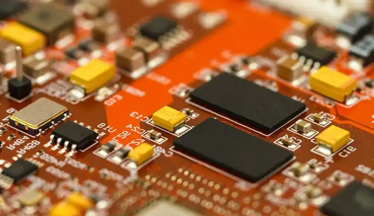
Material Selection for Consumer PCB Durability and Performance
When it comes to selecting materials for Consumer PCBs, it’s more than just choosing a board. The material needs to handle mechanical stress, temperature extremes, and electrical performance requirements. FR4, a common choice due to its balance of cost and functionality, is widely used. However, for high-performance applications such as wearables or automotive electronics, high-frequency laminates or ceramic substrates may be the better choice, as they provide better signal integrity and thermal management.
For flexible designs, flexible substrates like polyimide offer both the flexibility and durability needed for devices that need to bend, stretch, or fit into tight spaces.
| Material | Application | Advantages | Challenges |
| FR4 | General-purpose boards, consumer electronics | Cost-effective, reliable, widely available | Poor performance at high frequencies |
| Ceramic PCBs | High-performance, automotive, medical | Excellent thermal management, high signal integrity | More expensive, harder to process |
| High-Frequency Laminates | Communication devices, wearables | Superior signal performance at high speeds | Higher cost, limited availability |
| Flexible Substrates (Polyimide) | Wearables, flexible displays | Flexibility, heat resistance, lightweight | High manufacturing complexity |
By understanding the different PCB materials and their benefits, manufacturers can make better decisions about which materials best suit the specific needs of their Consumer PCB designs.
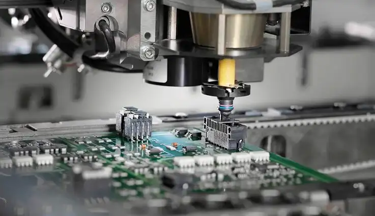
Surface Mount Technology (SMT) and Multilayer PCBs for Complex Designs
Surface Mount Technology (SMT) is like the secret sauce that makes Consumer PCB assembly a breeze. Instead of dealing with bulky components, SMT lets manufacturers mount parts right on the PCB’s surface. It’s perfect for gadgets like smartphones and wearables, where space is tighter than a drum. With SMT, you get more bang for your buck, cramming more tech into smaller packages. It’s the unsung hero of compact device design, giving manufacturers a leg up in a market that’s all about getting smaller, faster, and smarter.
Multilayer PCBs, where multiple conductive layers are stacked together and interconnected, further add to the design’s complexity. These boards are used in high-tech devices like tablets, laptops, and advanced automotive systems, as they allow for high circuit density without increasing board size.
| Feature | SMT Application | Multilayer PCB Application |
| Space Saving | Components mounted directly on the surface, saving board space | Stacked layers allow for dense circuit routing |
| Cost Efficiency | Reduces material costs by eliminating through-hole components | Allows for integration of complex designs |
| High-Density Components | Perfect for compact designs with advanced functionality | Supports high-performance applications |
| Design Complexity | Simpler, faster assembly for standard designs | More challenging assembly and testing processes |
SMT allows for faster, more efficient production, while multilayer PCBs enable the integration of advanced features into small, portable devices. Together, these techniques help create the powerful, compact Consumer PCBs we see in modern gadgets.
Advanced Testing and Quality Assurance for Reliable Consumer PCBs
After manufacturing, testing and quality assurance come into play to ensure that Consumer PCBs function as expected. The stakes are high; faulty boards can lead to product failures, customer dissatisfaction, and costly recalls. The goal is to ensure that every Consumer PCB meets both performance standards and industry regulations.
Automated Optical Inspection (AOI) is often the first line of defense, catching defects like misaligned components, soldering issues, or missing components. For more complex boards, X-ray inspection is used to check inner layers of the PCB for issues that are not visible on the surface. Testing also includes environmental tests to ensure RoHS compliance and other regulatory standards are met.
| Test Method | Purpose | Applications |
| Automated Optical Inspection (AOI) | Detects surface-level defects such as misalignment, soldering issues | Mass production lines for consumer electronics |
| X-ray Inspection | Inspects internal layers of the PCB for issues not visible on the surface | High-density or complex multilayer PCBs |
| Electrical Testing | Ensures that the PCB’s electrical performance matches design specifications | Used to verify signal integrity in high-frequency circuits |
| Environmental Testing | Tests PCBs for durability in extreme conditions (e.g., temperature, humidity) | Automotive, aerospace, and medical device PCBs |
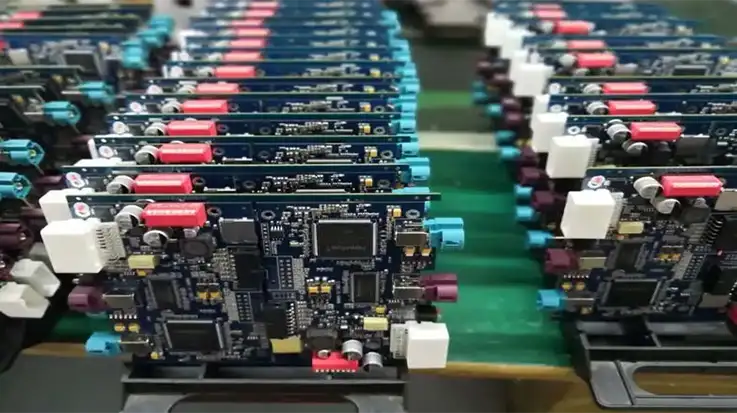
The Leading Chinese Consumer PCB Supplier
Back in the day, consumer electronics like white goods, brown goods, and smart toys were powered by simple, rigid PCBs with just 1-4 layers. But fast forward to today, and things have totally stepped up. We’re talking multi-layer HDI boards—sometimes six layers or more—and flexible or stiff-flex designs.These high-performance designs demand precise manufacturing and top-of-the-line tech. Things aren’t what they used to be, that’s for sure!
At JarnisTech, we’ve got your back when it comes to meeting the cutting-edge needs of your consumer PCB projects. Whether you’re creating the next big wearable gadget or innovating in the home appliance sector, we’re here to guide you from design to manufacturing. Thousands of electronic engineers trust JarnisTech to turn their visions into reality.
Why Choose JarnisTech?
JarnisTech stands out as the top Chinese consumer PCB manufacturer because we provide more than just PCBs—we deliver solutions. With our 24-hour rapid response service from both our tech support and sales team, you can rest easy knowing that any questions or concerns will be addressed promptly.
Our team’s experience with HDI, flexible, and rigid-flex PCBs means we can support your most demanding projects. No matter your design or production needs, we’ve got the equipment, knowledge, and resources to make it happen.
What Makes JarnisTech Stand Out?
1.Cutting-Edge Technology: From basic designs to advanced HDI, flexible, and rigid-flex PCBs, our technology ensures you get the highest quality boards. We stay ahead of the curve with the latest PCB design and manufacturing tools to meet the demands of consumer electronics.
2.Unmatched Support: Our rapid response service isn’t just about speed; it’s about having a team ready to provide expert advice, solve issues, and ensure your production goes off without a hitch. Questions? Our tech support and sales teams are available 24/7 to guide you through any stage of the process.
3.Customization: At JarnisTech, we understand that each consumer PCB project is unique. Whether you’re working with complex HDI boards or looking for flexible PCB solutions, we have the experience and flexibility to tailor our services to your specific needs.
4.Reliable and Scalable Production: We don’t just handle prototypes; we’re ready for large-scale production too. Our advanced facilities allow us to manage everything from small runs to high-volume orders without compromising quality.
Table of Key Services
| Service | What We Offer | Why It’s Beneficial to You |
| Advanced PCB Technology | HDI, flexible, rigid-flex boards, multi-layer designs | High-performance PCBs that meet the latest consumer electronics standards |
| 24-Hour Support | Rapid response from tech support and sales teams | Get fast, expert solutions at every step of your project |
| Tailored Solutions | Customization options for all types of PCBs | PCBs designed specifically for your unique product needs |
| Scalable Production | Capable of handling low-volume prototyping to large-scale orders | Flexibility to scale up production as your business grows |
JarnisTech is your trusted partner in turning consumer electronics ideas into reality. With cutting-edge technology, expert support, and reliable production capabilities, we’re equipped to tackle even the most challenging PCB projects. So, don’t hesitate to reach out—whether it’s for a quick question or a full-scale production run, we’re ready to work with you to create the best PCBs for your business. Let’s make your next project a success together!
Regulatory Compliance and Environmental Considerations for Consumer PCBs
As Consumer PCBs become more integral to modern electronics, ensuring that they comply with various regulations has become more important than ever. Manufacturers must stay on top of ever-evolving standards like RoHS (Restriction of Hazardous Substances) and WEEE (Waste Electrical and Electronic Equipment), which dictate the use of specific materials and the safe disposal of electronics. These standards have significant implications for PCB production and environmental sustainability.
Ensuring RoHS Compliance and Lead-Free Assembly in Consumer PCBs
In today’s eco-conscious market, RoHS compliance is a must for Consumer PCB manufacturers. RoHS regulations restrict the use of hazardous substances like lead, mercury, cadmium, and hexavalent chromium in electrical and electronic products. These regulations are especially strict in regions like the European Union, and manufacturers must ensure that their products are RoHS-compliant to access these markets.
Lead-free assembly is one of the primary components of RoHS compliance. This process involves using lead-free solders, which, while posing their own challenges, help reduce the environmental impact of electronics. By transitioning to lead-free soldering and adopting alternative materials like silver, copper, or tin for solder joints, manufacturers can reduce their carbon footprint and avoid potential health hazards related to toxic metals.
Lead-free PCB assembly also opens up the possibility of meeting global market standards and gaining access to industries that prioritize sustainability and environmental stewardship. Furthermore, using lead-free technology often improves the reliability and performance of Consumer PCBs, thanks to the advanced materials that replace lead-based solder.
| Hazardous Substance | RoHS Limit | Lead-Free Alternative | Benefits |
| Lead (Pb) | 0.1% | Silver, Copper, Tin | Reduced environmental impact, safer production |
| Mercury (Hg) | 0.1% | None (typically avoided) | Reduced risk to health and environment |
| Cadmium (Cd) | 0.01% | None (typically avoided) | Eliminates carcinogenic risks |
| Hexavalent Chromium | 0.1% | None (typically avoided) | Reduces environmental contamination |
DFM and DFA: Optimizing Consumer PCB Design for Manufacturability and Assembly
When designing Consumer PCBs, the goal is to make sure that the boards are not just high-performance but also simple to manufacture and assemble. That’s where methodologies like Design for Manufacturability (DFM) and Design for Assembly (DFA) really kick in. These approaches are all about cutting down on complexity, making sure everything fits like a glove, and helping the whole production process run like clockwork. This keeps costs low and speeds up those crucial timelines.
DFM focuses on designing the PCB with manufacturing constraints in mind. The goal is to minimize the number of complex steps in the production process, reducing errors and rework. By simplifying the design, manufacturers can reduce the number of materials needed, speed up production, and ultimately lower costs.
On the other hand, DFA aims to simplify the assembly process. It looks at the ease with which components can be mounted, soldered, and tested on the PCB. By designing for easy assembly, manufacturers can reduce labor costs, lower the risk of errors, and streamline the overall assembly process.
| Method | Focus Area | Benefits | Applications |
| DFM | Simplify the manufacturing process | Lower costs, reduce production time | High-volume production of consumer electronics |
| DFA | Simplify the assembly process | Minimize assembly errors, reduce labor | Devices with complex designs and small components |
| Integrated DFM/DFA | Combine both methods to optimize overall design | Achieve maximum efficiency in both manufacturing and assembly | Used in high-tech industries like smartphones and wearables |
When designers implement DFM and DFA, they’re not just greasing the wheels of the process, they’re also making sure the assembly goes off without a hitch. This means faster production times, fewer errors, and less cost, which can make or break a product in today’s ultra-competitive consumer electronics world. These methods help manufacturers keep the gears turning without unnecessary roadblocks, allowing them to hit deadlines while keeping the bottom line in check. It’s all about working smarter, not harder.
Procurement Strategies for Consumer PCBs
After wrapping up the design and manufacturing phases, it’s time to talk procurement. Now, this isn’t just about grabbing the cheapest deal—it’s about finding a supplier who’s got your back in terms of quality, cost, and getting things done on time. If you think you can get by with any supplier off the shelf, think again. You need one that’s rock-solid when it comes to delivery, quality, and keeping things running like clockwork.
How to Choose the Right Consumer PCB Suppliers?
Choosing the right PCB supplier isn’t a “one-size-fits-all” deal. It’s not all about price, folks—it’s about picking a supplier who delivers the goods every time. Quality? Check. Timely delivery? Check. The ability to scale with your growing needs? Check, check, check.
You want a turnkey supplier—someone who’s got the whole shebang covered, from prototyping to full-blown production. This way, you don’t have to juggle multiple vendors and can focus on what really matters: getting your product to market.
Look, not every supplier is going to cut it. You’ll need to evaluate them beyond just price. Think reputation, customer support, and whether they can deliver exactly what you need without any drama. A reliable supplier is like a good business partner—someone who’s got your back when things get tight.
| Evaluation Criteria | Description | Why It Matters |
| Reliability | How consistently the supplier delivers quality products on time. | Keeps production schedules on track. |
| Quality Assurance | Processes in place to ensure defect-free products (e.g., visual inspection, testing). | Reduces risks of defective products. |
| Turnkey Services | Supplier offers both prototyping and full-scale production. | Streamlines procurement and reduces vendor management. |
| Reputation & Reviews | Customer feedback on their products and services. | Provides insight into long-term reliability. |
| Cost Competitiveness | The pricing structure based on order volume and additional value-added services. | Helps maintain budget-friendly procurement. |
Cost Efficiency and Volume Procurement for Consumer PCBs
When it comes to procurement, balancing costs and volume is the name of the game. You need to figure out when it makes sense to go big or stay small, depending on whether you’re doing a low-volume, high-mix run or a high-volume, low-mix production. It’s all about making those cost-effective choices without breaking the bank.
For low-volume, high-mix, you’re looking at small batches with higher flexibility. It’s perfect for that quick turnaround on prototypes or custom designs. On the flip side, high-volume production is your sweet spot when you’re looking to churn out thousands of units at a cheaper per-unit price. The beauty here is the economy of scale.
It’s not just about the raw numbers—it’s about collaboration. Get with your suppliers, figure out the real-time demand, and align your strategy with their capabilities. That’s how you keep costs low without sacrificing flexibility.
| Procurement Type | Volume Range | Flexibility Needed | Cost Efficiency | Ideal Application |
| Low-Volume, High-Mix | Small batches (50-1000) | High (frequent design changes) | Moderate to high due to the complexity of varied orders | Prototypes, limited edition products, and custom designs |
| High-Volume, Low-Mix | Large batches (10,000+) | Low (stable designs) | Very high due to economies of scale | Mass production of consumer electronics |
| Medium-Volume, Medium-Mix | Moderate batches (1000-10,000) | Moderate flexibility | Balanced cost-efficiency | Mid-range production, wearables, etc. |
Why JarnisTech Should Be Your First Choice for Consumer Electronics PCB Needs?
1. State-of-the-Art Facility: Cutting-Edge Technology at Your Service
At JarnisTech, we’re not just another PCB provider—we’ve built a reputation for staying ahead of the curve in the consumer electronics space. Our advanced facility is fully equipped with the latest in PCB manufacturing technology. From design to assembly, we leverage industry best practices to ensure your PCBs meet the highest standards. Whether you’re dealing with high-frequency signals or complex multi-layer designs, we’ve got the tools to bring your product to life with precision and efficiency. It’s like having a top-tier engineering team right in your corner, ready to tackle any challenge!
Example: For instance, when our team worked on high-performance boards for a leading smart home device, our precision machinery ensured flawless connectivity across multiple layers and components, making sure the product met the market’s demands.
2. Stringent Manufacturing Procedures: Quality Without Compromise
At JarnisTech, we understand that when it comes to consumer electronics, reliability is king. That’s why we adhere to strict manufacturing protocols. Our stringent quality control measures ensure that every PCB we produce is tested for performance, durability, and longevity. From pre-production prototypes to final assembly, we make sure nothing slips through the cracks.
Every board undergoes thorough inspection, stress tests, and reliability checks to guarantee that you’re getting a product that’s built to last. Our no-compromise approach gives you peace of mind, knowing your PCBs will stand the test of time in even the most demanding applications.
Example: During the production of a consumer audio device, our quality control checks identified a minor flaw in a batch of boards, which we promptly corrected, saving our client from costly product recalls.
3. Fast Turnaround: Get Your Products to Market Quicker
In the consumer electronics market, speed can make or break a product launch. That’s why we offer rapid turnaround times without sacrificing quality. With JarnisTech, you’ll never be caught in the slow lane. We know how critical it is to get your product out there before the competition does. Our fast and efficient processes allow us to move quickly from design to delivery, ensuring you can launch your product faster than ever.
Our experienced team works around the clock to keep things on track, so you can focus on innovation while we handle the heavy lifting. Whether you need to meet tight deadlines or adjust to changes in project scope, JarnisTech is there to support you every step of the way.
Example: One of our clients needed a quick PCB prototype for a new wearable device to showcase at a major tech conference. Thanks to our rapid turnaround time, they received their boards on time, allowing them to present their product on schedule and land a deal with a major retailer.
4. No Volume Restrictions: Flexibility for Your Project’s Needs
Whether you need a small batch of prototypes or large-scale production, JarnisTech has the capacity and flexibility to meet your needs. We don’t believe in “one-size-fits-all”—instead, we tailor our services to match your unique requirements, whether you’re scaling up for mass production or testing out a new design.
Our production capabilities are scalable, so you don’t have to worry about volume restrictions. From low-volume, high-mix runs to high-volume production, we can handle it all with the same level of precision and quality.
Example: We’ve worked with startups who needed small batches for market testing and also helped established brands scale up for large product launches. No matter the size of the order, we ensure that each batch meets the same high-quality standards.
Table of Services and Capabilities
| Feature | What We Offer | Benefits to You |
| State-of-the-Art Technology | Advanced manufacturing equipment and design tools | High precision, high-quality PCBs in complex designs |
| Stringent Testing Procedures | Rigorous quality control checks and stress testing | Reliable, durable boards that stand the test of time |
| Fast Turnaround | Rapid production times, even for complex designs | Get your products to market faster and outpace the competition |
| No Volume Restrictions | Flexible production capabilities from small batches to large runs | Perfect for prototyping and scaling up production seamlessly |
Choosing JarnisTech means more than just finding a PCB supplier—it’s about partnering with a team that’s dedicated to helping you succeed. From quick prototypes to large-scale production runs, our team works tirelessly to meet your needs, ensuring you get high-quality, reliable PCBs every time. So, let’s get the ball rolling—contact JarnisTech today and see how we can help bring your consumer electronics projects to life!
FAQ about Consumer PCBs
What is a Consumer PCB?
A consumer PCB is a type of printed circuit board used in various consumer electronic devices like smartphones, wearables, and home appliances.
What are the types of PCBs used in consumer electronics?
Common types include single-sided, double-sided, multi-layer, rigid, flexible, and HDI (High-Density Interconnect) boards.
Why are flexible PCBs important in consumer electronics?
Flexible PCBs allow for more compact, lightweight, and durable designs, which are ideal for modern portable devices.
What materials are typically used in consumer PCBs?
Common materials include FR4 (fiberglass), ceramic, and high-frequency laminates, with newer materials being used for flexibility and high-speed signal applications.
What is RoHS compliance for consumer PCBs?
RoHS compliance ensures that PCBs are free from hazardous substances like lead and mercury, adhering to environmental regulations.
What is the typical lifespan of a Consumer PCB?
The lifespan depends on the materials used, the quality of manufacturing, and the environment in which the PCB is used. High-quality PCBs can last many years with proper use.


