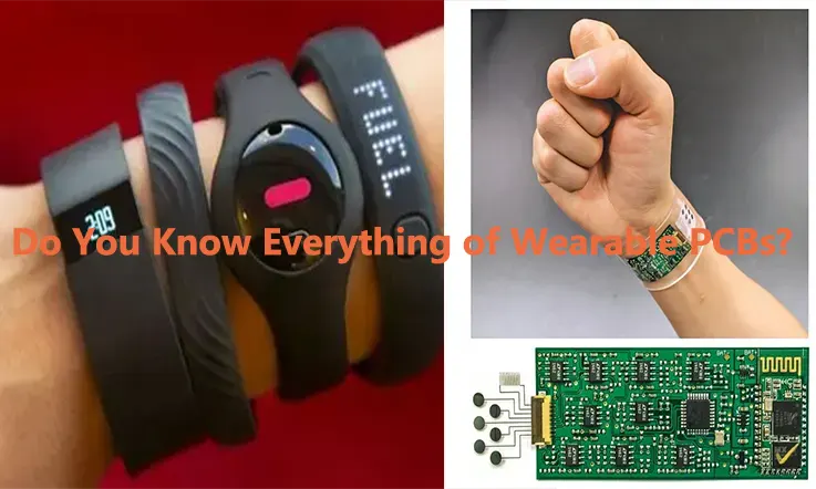
In recent years, the popularity of wearable devices has soared, propelled by remarkable advancements in the electronics industry and the availability of highly integrated electronic components that offer enhanced efficiency, performance, and compactness. At the core of each wearable device, whether it’s a smartwatch, fitness tracker, or electro-medical device (EMD), lies a printed circuit board (PCB) whose design presents a formidable challenge for electronic engineers. Creating a successful wearable device necessitates meeting a range of requirements, including small form factor, lightweight construction, low power consumption, reliability, and minimal heat generation.
Given their exceptionally compact size and relatively recent emergence in the market, there is no established standard specifically tailored to PCB design for wearable devices. However, it is possible to leverage techniques and recommendations that apply to circuits with similar characteristics, drawing on the expertise gained from the development and production of advanced PCBs.
Overview of Wearable Technology
Wearable technology refers to electronic devices that can be worn on the body, typically as accessories or clothing items. These devices are designed to provide functionality and connectivity while being convenient and seamlessly integrated into daily life.
Wearable technology has gained significant popularity in recent years due to advancements in miniaturization, sensor technology, wireless connectivity, and computing power. It has found applications in various fields, including fitness and health monitoring, communication, entertainment, fashion, and industrial sectors.
Key Features and Functions of Wearable Technology
Sensing and Monitoring: Wearable devices often incorporate sensors to monitor various aspects of the user’s body and environment. These sensors can include heart rate monitors, accelerometers, gyroscopes, GPS, temperature sensors, and more.
Data Collection and Analysis: Wearable devices collect data from the sensors and process it to provide meaningful insights to the user. This data can include activity levels, sleep patterns, biometric measurements, location information, and more.
Connectivity: Most wearable devices are equipped with wireless connectivity options such as Bluetooth, Wi-Fi, or cellular connectivity. This allows them to communicate with smartphones, tablets, or other devices, enabling data transfer, notifications, and remote control functionalities.
User Interface: Wearable devices utilize various user interface options to interact with the wearer. This can include touchscreens, buttons, voice commands, gestures, or a combination of these elements.
Integration with Mobile Devices and Applications: Many wearable devices are designed to work in tandem with smartphones or other mobile devices. They often have companion apps that enable data synchronization, customization, and extended functionalities.
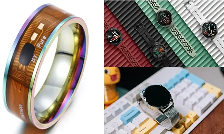
Examples of Wearable Technology
Fitness Trackers: These devices, such as fitness bands or smartwatches, monitor physical activities, track steps, calories burned, sleep patterns, and heart rate. They provide insights for fitness and health management.
Smartwatches: These wrist-worn devices offer features beyond timekeeping. They can display notifications, allow phone calls, track fitness metrics, control music playback, and run various apps.
Augmented Reality (AR) and Virtual Reality (VR) Headsets: These devices immerse users in virtual or augmented environments, providing an interactive and immersive experience for gaming, education, training, or entertainment purposes.
Smart Clothing: Certain garments incorporate sensors and electronic components for tracking biometrics, posture, or environmental factors. They can be used in sports, healthcare, or fashion industries.
Smart Glasses: These glasses feature built-in displays, cameras, and sensors, enabling hands-free access to information, navigation assistance, and augmented reality overlays.
Medical Wearables: Wearable devices in the medical field include devices for continuous glucose monitoring, blood pressure monitoring, sleep apnea tracking, and more.
The field of wearable technology is constantly evolving, with ongoing advancements in materials, battery life, connectivity, and functionality. It holds promising potential for enhancing personal well-being, improving productivity, and transforming various industries.
What Is wearable PCB?
A wearable PCB (Printed Circuit Board) refers to a circuit board that is specifically designed to be integrated into wearable devices, such as smartwatches, fitness trackers, smart clothing, and other wearable gadgets. PCBs are essential components of electronic devices as they provide a platform for connecting and mounting electronic components, such as microchips, sensors, and other circuitry.
In the context of wearables, PCBs are miniaturized and flexible to accommodate the unique form factors and requirements of wearable devices. They are typically lightweight, thin, and bendable to conform to the shape of the wearable product or fit within the available space. This flexibility allows PCBs to be integrated into garments, accessories, or directly onto the human body.
Wearable PCBs are designed to provide electrical connectivity between various components within the wearable device. They enable the transfer of power, data signals, and control signals between the microcontroller, sensors, display, battery, and other components. The PCB layout and design are optimized for efficient power consumption, reliable data transmission, and compactness.
Wearable PCBs often incorporate advanced technologies like surface mount components, ultra-thin conductive traces, and multi-layered designs to maximize functionality while minimizing size and weight. They may also integrate additional features like wireless connectivity (Bluetooth, Wi-Fi), charging circuits, and power management systems.
Overall, wearable PCBs play a crucial role in enabling the functionality and performance of wearable devices, allowing them to perform various tasks such as monitoring health data, tracking activity, displaying information, and connecting to other devices or networks.
Wearable PCB Types
Wearable PCBs (Printed Circuit Boards) can come in various types depending on the specific requirements and design considerations of the wearable device. Here are some common types of wearable PCBs:
Rigid PCBs
Rigid PCBs are the most common type of PCB used in wearables. They have a solid substrate made of rigid materials like fiberglass or epoxy resin. Rigid PCBs provide stability and support to the wearable device.
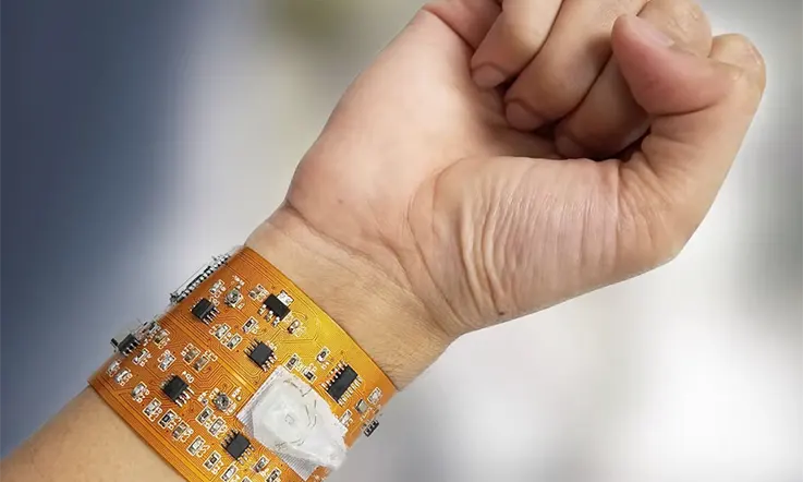
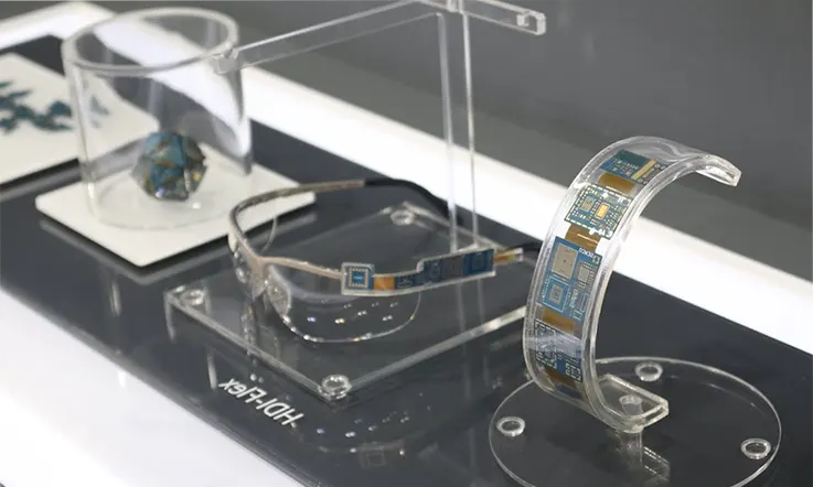
Flexible PCBs
Flexible PCBs are designed to bend and flex, making them suitable for wearable devices that require flexibility. They are made of flexible materials like polyimide or polyester. Flexible PCBs allow for shape conformity, making them ideal for wearables that need to conform to the body or an irregular surface.
Benefits of Flexible PCBs in Wearable Devices:
Size and Weight Reduction: Flexible PCBs can be designed to be thin, lightweight, and highly flexible, allowing them to conform to the shape of the wearable device. This property makes them ideal for space-constrained wearables where size and weight reduction are crucial factors.
Flexibility and Bendability: As the name suggests, flexible PCBs can be bent, twisted, and folded without damaging their functionality. This flexibility enables the design of wearable devices that can conform to the contours of the human body or fit into unconventional shapes.
Increased Reliability: Flexible PCBs have fewer interconnects and solder joints compared to rigid PCBs, reducing the risk of interconnection failures. The absence of connectors and cables also minimizes the likelihood of disconnections or breakages, enhancing the overall reliability of wearable devices.
Enhanced Durability: Wearable devices often encounter bending, stretching, or twisting motions during use. Flexible PCBs can withstand these mechanical stresses without compromising their electrical performance, leading to increased durability and longer product lifecycles.
Improved Thermal Management: Flexible PCBs have excellent thermal dissipation properties, allowing for efficient heat transfer. This feature is essential in wearables that generate heat, such as smartwatches or fitness trackers, ensuring proper functioning and preventing overheating.
Applications of Flexible PCBs in Wearable Devices:
Smartwatches: Flexible PCBs can be used in smartwatches to enable the display, touch sensors, microcontrollers, and other components to flex with the shape of the wristband. This ensures a comfortable fit and seamless integration of electronics into the device.
Fitness Trackers: Flexible PCBs are well-suited for fitness trackers due to their ability to conform to the contours of the body. They can be integrated into wristbands, chest straps, or other wearable forms, accommodating various sensors and connecting them to the main processing unit.
Medical Wearables: Flexible PCBs find applications in medical wearables like health monitoring devices, ECG monitors, and smart medical patches. Their flexibility allows for comfortable and non-intrusive integration into garments or adhesion to the skin, enabling continuous health monitoring.
Smart Clothing: Flexible PCBs can be integrated into smart clothing, such as sports apparel or safety garments. They enable the integration of sensors, LEDs, or communication modules while maintaining the flexibility and washability of the fabric.
Head-Mounted Displays (HMDs): Flexible PCBs play a crucial role in headsets or augmented reality glasses. They facilitate the connection of display panels, sensors, microcontrollers, and other components while maintaining the lightweight and ergonomic design required for comfortable use.
Stretchable PCBs
Stretchable PCBs are an advanced type of wearable PCB that can stretch and deform without damage to the circuitry. They are typically made using stretchable materials and can be integrated into wearable devices that require stretchability, such as smart clothing or healthcare monitoring devices.
Hybrid PCBs
Hybrid PCBs combine rigid and flexible sections on the same board. They provide a combination of stability and flexibility, allowing for more versatile designs. Hybrid PCBs are often used in wearables that require both rigid and flexible components, such as smartwatches or fitness trackers.
Chip-on-Board (COB) PCBs
COB PCBs involve directly mounting bare semiconductor chips on the PCB substrate without using traditional packaged components. This integration technique reduces the size and weight of the PCB, making it suitable for miniaturized wearable devices.
Multi-layer PCBs
Multi-layer PCBs consist of multiple layers of conductive traces and insulating materials stacked together. They provide more complex interconnectivity and allow for the integration of more components in a compact space. Multi-layer PCBs are commonly used in advanced wearable devices that require higher functionality and performance.
These are just a few examples of wearable PCB types. The choice of PCB type depends on factors such as the form factor, flexibility requirements, power considerations, and the specific functionality of the wearable device. Different types of PCBs offer different advantages and trade-offs, and the selection is usually based on the specific needs of the wearable device.
Challenges in Wearable PCB Design
Designing PCBs for wearable devices presents unique challenges due to the small form factor, power constraints, mechanical considerations, and the need for reliable and robust performance. Here are some common challenges in wearable PCB design:

Size and Form Factor Constraints: Wearable devices are typically small and compact, making it challenging to fit all the necessary components onto the PCB. Designers need to carefully consider component placement, routing, and stack-up strategies to optimize space utilization while ensuring functionality and reliability.
Power Management and Energy Efficiency: Wearable devices often have limited battery capacity and need to operate for extended periods without recharging. PCB designers must focus on power management techniques, such as low-power components, efficient power conversion circuits, and power-saving modes to maximize battery life and optimize energy consumption.
Mechanical and Environmental Considerations: Wearable devices are subjected to various movements, vibrations, and environmental conditions. The PCB design should account for mechanical stress, flexing, and temperature variations. Special consideration must be given to the selection of materials, component mounting techniques, and solder joint reliability to ensure the PCB can withstand the demands of the wearable application.
Interconnectivity and Communication Requirements: Many wearable devices rely on wireless connectivity, such as Bluetooth or Wi-Fi, to communicate with other devices or transmit data to the cloud. PCB designers need to integrate reliable and robust wireless communication modules and antennas into the PCB design, considering signal integrity, interference, and electromagnetic compatibility (EMC) issues.
Sensor Integration and Signal Conditioning: Wearable devices often incorporate various sensors to collect data from the wearer’s body or the surrounding environment. PCB designers must carefully integrate these sensors into the design, ensuring proper signal conditioning, noise reduction, and accurate data acquisition.
Design for Manufacturing (DFM) and Assembly: PCBs for wearable devices often require specialized manufacturing and assembly processes due to their small size and complexity. Designers must consider DFM guidelines, such as panelization, solder mask requirements, and component accessibility, to facilitate efficient and cost-effective production.
User Experience and Ergonomics: Wearable devices are meant to be comfortable and convenient for users. PCB designers need to collaborate closely with industrial designers to ensure that the PCB layout, component placement, and overall design contribute to a positive user experience, including comfort, aesthetics, and ease of use.
Addressing these challenges requires a multidisciplinary approach, involving collaboration between PCB designers, electrical engineers, mechanical engineers, industrial designers, and other stakeholders. Advanced simulation and design tools can also aidin overcoming these challenges by enabling virtual prototyping, signal integrity analysis, thermal analysis, and mechanical simulations to optimize the wearable PCB design before physical production.
How to Fabrication a Wearable PCB ?
Fabricating a wearable PCB (Printed Circuit Board) involves several steps. Here’s a general overview of the process:
Design the PCB: Begin by creating a PCB design using specialized software like Altium, Eagle, or KiCad. Consider the form factor and space constraints of the wearable device. Design the PCB layout, including component placement, signal routing, and power distribution.
Prototype and test: Before moving to mass production, it’s advisable to create a prototype PCB to verify the design and functionality. Use a PCB prototyping service or manufacture a small batch of PCBs using your preferred fabrication method. Test the prototype for electrical performance, functionality, and fit within the wearable device.
Choose a fabrication method: Select the appropriate fabrication method based on your budget, quantity, and complexity requirements. Common methods include:
● PCB fabrication houses: Send your PCB design files to a professional PCB fabrication house. They will manufacture the PCBs based on your specifications, using processes like etching, drilling, and copper plating. This method is ideal for larger production quantities.
● PCB prototyping services: If you require a small batch or quick turnaround, consider using PCB prototyping services. These services offer faster fabrication with shorter lead times but may have higher per-unit costs compared to larger-scale manufacturers.
● In-house fabrication: For small-scale production or prototyping, you can fabricate PCBs in-house using DIY methods like toner transfer, milling, or 3D printing. This approach is suitable for low-complexity designs and limited quantities.
Generate manufacturing files: Prepare the necessary files for PCB fabrication. These typically include Gerber files, which contain the layer information, copper traces, solder mask, and silkscreen, as well as drill files for creating holes.
Order fabrication: Place an order with the chosen fabrication service or manufacturer. Provide the necessary design files and specifications, including the desired quantity, material choice (FR-4 is common for PCBs), board thickness, copper weight, and surface finish (e.g., ENIG or HASL).
Fabrication process: The fabrication service or manufacturer will process your order. The steps involved may vary depending on the chosen fabrication method. Generally, the process involves:
● Preparing the PCB panel: The design files are used to create a panel that contains multiple PCBs. The panel is typically made of a larger board, and multiple PCBs are fabricated simultaneously to improve efficiency.
● Etching: A chemical process is used to remove the unwanted copper from the PCB, leaving behind the desired copper traces.
● Drilling: Holes for component mounting and vias are drilled into the PCB.
● Copper plating: A thin layer of copper is plated onto the PCB’s exposed copper surfaces, improving conductivity and protecting the traces.
● Solder mask and silkscreen application: A solder mask is applied to protect the copper traces, and a silkscreen layer is added for component labeling and identification.
● Electrical testing: The fabricated PCBs undergo electrical testing to ensure their functionality and integrity.
Assembly and component placement: Once the PCBs are fabricated, the next step is to assemble the components. This involves soldering surface-mount and through-hole components onto the PCB. Depending on the complexity of the components and the volume of production, you can choose manual soldering or automated assembly methods.
Testing and quality control: Conduct thorough testing to verify the functionality and performance of the assembled wearable PCBs. Use testing equipment like multimeters, oscilloscopes, or functional testers to ensure the PCBs meet the desired specifications. Implement quality control measures to identify and rectify any defects or issues.
Integration into wearable device: Once the wearable PCBs pass testing and quality control, integrate them into the wearable device according to the design requirements. Ensure proper connectivity, alignment, and mechanical support for the PCB within the wearable product.
Final testing and packaging: Perform a final round of testing on the assembled wearable device to ensure everything functions as intended. Once the device passes testing, package it appropriately for shipping or distribution.
It’s worth noting that the fabrication process can vary depending on the complexity of the wearable PCB design, the chosen materials and technologies, and the specific requirements of the wearable device. Working with experienced PCB manufacturers or assembly houses can provide valuable guidance and assistance throughout the fabrication process.
How to Select the Material for Wearable PCB?
When selecting materials for a wearable PCB, several important factors should be taken into consideration to ensure optimal performance. These factors include high reliability, high speed and frequency capabilities, limited power losses, reduced production cost, and a stable coefficient of thermal expansion. By considering these aspects, you can ensure that the wearable PCB meets the specific requirements of the application. To assist you in this process, JarnisTech is a recommended supplier known for providing wearable PCBs made from materials that possess all the desired characteristics.
Reliability is a critical aspect to consider when choosing materials for a wearable PCB. It is essential for the material to exhibit a high degree of reliability to ensure the longevity and functionality of the device. By selecting materials known for their reliability, you can minimize the risk of failure and enhance the overall performance of the wearable PCB.
Another key consideration is the ability of the material to support high-speed and high-frequency signals. Traditional materials like FR4 may not be suitable for this purpose, as they may introduce signal degradation. Hence, it is advisable to explore advanced materials that are specifically designed to handle high-speed and high-frequency signals, thereby maintaining the integrity of the data transmitted within the wearable PCB.
The material’s power loss characteristics are also crucial, particularly when dealing with high-frequency signals. To minimize power losses, materials such as Rogers 4350 are recommended. Rogers 4350 exhibits superior electrical properties, enabling efficient transmission of signals while minimizing power losses. By utilizing materials with limited power losses, the wearable PCB can achieve higher efficiency and performance.
Cost-effectiveness is another factor to be mindful of during material selection for wearable PCBs. Manufacturing wearable PCBs at a reduced production cost is advantageous for businesses. For this reason, alternatives like Rogers are often preferred over FR4, as they offer a balance between performance and cost. By choosing materials that strike a favorable balance between quality and affordability, you can optimize the production process of wearable PCBs.
Finally, the material should possess a stable coefficient of thermal expansion to withstand high temperatures. Wearable devices can be subjected to varying environmental conditions, including temperature fluctuations. Therefore, selecting a material with a stable coefficient of thermal expansion ensures that the wearable PCB can endure temperature changes without compromising its integrity or functionality.
What are Fabrication Issues in Wearable PCBs?
Fabrication challenges in wearable PCBs include:
Impedance Control for Wearable Devices
One of the most prevalent fabrication issues in wearable PCBs is achieving precise impedance control. This is crucial as it ensures efficient signal transmission within the device, resulting in improved performance.
Insertion Loss
To address insertion loss concerns, high-quality materials with reasonable tolerance levels are employed during fabrication. This helps minimize the loss of signal strength and maintain optimal performance.
Cost-Effectiveness
Cost-effectiveness is a significant consideration in the fabrication process. Therefore, the utilization of Rogers materials is favored due to their ability to offer low laminate loss. This choice helps strike a balance between performance and affordability.
Frequency Maintenance
Rogers laminates are commonly employed to uphold desired frequency characteristics. These materials exhibit superior impedance control, ensuring reliable signal transmission and minimizing disruptions caused by frequency variations.
Coefficient of Thermal Expansion
To ensure dimensional stability and mitigate issues related to the coefficient of thermal expansion, the use of Rogers 4000 series laminates is prominent. These laminates possess properties that effectively address the demands of wearable PCBs, enabling greater stability and reliability.
By addressing these fabrication challenges in a professional manner, wearable PCBs can be manufactured to meet the high standards required for optimal performance and functionality.
The Importance of Good Electronic Contract Manufacturers in the Wearable PCB Industry
Good electronic contract manufacturers (ECMs) play a crucial role in the wearable PCB (Printed Circuit Board) industry. PCBs are the backbone of electronic devices, including wearables, as they provide the necessary connectivity and functionality. Here are some reasons why good ECMs are important in the wearable PCB industry:
Design expertise: Wearable devices often have unique form factors and space constraints, requiring customized PCB designs. Good ECMs have experienced design teams that understand the specific requirements of wearable devices. They can optimize the PCB layout to fit within the limited space while ensuring efficient signal routing, thermal management, and electrical performance.
Manufacturing capabilities: ECMs with expertise in the wearable PCB industry possess advanced manufacturing capabilities necessary for producing high-quality PCBs. They have state-of-the-art equipment for surface mount technology (SMT), fine pitch component placement, and precision soldering, ensuring accurate assembly of small and densely packed components on the PCBs.
Miniaturization and flexibility: Wearable PCBs need to be small, lightweight, and flexible to fit into wearable form factors such as smartwatches, fitness bands, or smart clothing. Good ECMs have experience in miniaturization techniques and can manufacture flexible PCBs, rigid-flex PCBs, or other specialized PCB types required for wearables. They understand how to optimize the design and manufacturing process to achieve the desired size, weight, and flexibility characteristics.
Quality control and reliability: Wearable devices are subjected to various physical stresses, including bending, stretching, and moisture exposure. Good ECMs implement strict quality control measures throughout the manufacturing process to ensure the reliability and durability of the wearable PCBs. They conduct thorough testing, including functional testing, electrical testing, and environmental testing, to identify and rectify any defects or issues.
Component sourcing and supply chain management: ECMs with established relationships with component suppliers can help wearable companies in sourcing high-quality components at competitive prices. They have the expertise in managing the supply chain, ensuring timely availability of components for PCB assembly. Effective supply chain management minimizes production delays and helps wearable companies meet their deadlines.
Cost optimization: Good ECMs can provide cost optimization strategies during the PCB manufacturing process. They have the knowledge and experience to suggest design modifications or alternative components that can help reduce the overall manufacturing cost without compromising quality or functionality. This can be particularly beneficial for wearable companies operating in a competitive market.
Compliance and certification: Wearable devices may need to comply with industry regulations and certifications, such as RoHS (Restriction of Hazardous Substances) or FCC (Federal Communications Commission) certifications. Good ECMs have experience in navigating these regulatory requirements and can assist wearable companies in ensuring compliance. They can provide the necessary documentation and support during the certification process, saving time and effort for the wearable company.
Therefore, good electronic contract manufacturers are essential in the wearable PCB industry due to their expertise in PCB design, manufacturing capabilities, miniaturization techniques, quality control, supply chain management, cost optimization, and compliance support. Collaborating with the right ECM enables wearable companies to produce high-quality, reliable, and technologically advanced PCBs for their wearable devices, contributing to the success of their products in the market.
Why Choose JarnisTech for Your Wearable PCB
JarnisTech stands as a prominent wearable PCB manufacturer in China, renowned for its expertise in manufacturing high-quality boards that align with advanced production equipment. Backed by a team of skilled technical professionals, we offer a comprehensive solution for your project requirements.
Partnering with JarnisTech guarantees access to top-notch wearable PCBs and exceptional service, effectively contributing to the growth of your business. Whether your order is small or large in quantity, we are committed to delivering attentive and accommodating service. We invite you to promptly share your inquiries with us, allowing us to initiate a mutually beneficial collaboration.
Related Posts:
2. Drone PCB: Features, Types, Software, Design, Manufacturing and Choosing the Best Board