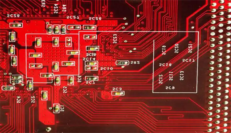
PCB, also known as printed circuit boards (also known as printed wiring board, or PWB), is a material employed in electronics and electrical technology for connecting electronics to each other in a controlled way. It’s an insulated sandwich consisting of insulating and conductor layers. Each of the conductive layers is created with an artistic pattern of planes, traces, and other elements (similar to wires on flat surfaces) made from one or more sheets of copper that are laminated on or between sheets of a non-conductive substrate.
The electrical components can be attached to conductive pads on the outer layer in a manner that is designed to accommodate terminals of the component, usually through soldering to connect them electrically and mechanically secure them to the substrate. Another process of manufacturing adds vias which are plated through holes that permit interconnections between layers.
Printed circuit boards(PCB) that are utilized in almost every electronic product. Alternatives to PCBs comprise wire wrap and point-to-point construction, which were both popular, but are now not used anymore. PCBs require additional design work to layout the circuit. However, manufacturing and assembly are processes that can be automated. Electronic design automation software can complete the majority of designing.
Due to the fact that components are mounted and wired in one step, PCBs are cheaper and faster than other methods of wiring circuits for mass production. It is possible to fabricate a large number of PCBs at the same time, and the layout only needs to be done once. It is also possible to manually make PCBs in small quantities, with reduced benefits.
PCBs may either be single-sided (one copper layer) or dual-sided (two layers of copper on each side of the substrate layer) as well as multiple-layer (outer and inside layers of copper in combination with layers of the substrate). Multi-layer PCBs can provide a greater density of components, as circuit lines on the inner layers could consume the area between components. The popularity increase of multilayer PCBs that have more than two and particularly that have more than four copper planes was accompanied by the introduction of surface mount technology. However, multilayer PCBs can make repair, analysis, and field modification of circuits more challenging and generally difficult to implement.
Step-by-Step PCB Design Guidance
From the first sketches through the final design files, Here are the ten steps to design the printed circuit board:
Know The Electrical Parameters: Step 1
Before beginning the process of creating a PCB design, you must be aware of and comprehend the electrical characteristics of the design, which include:
● Voltages.
● Types of signal.
● Capacitance limits.
● Current maximums.
● Impedance characteristics.
● Shielding-related considerations.
● Comprehensive net wire list and a schematic.
● Type and the location of circuit components and connectors.
The Schematic Is Created: Step 2
One of the initial steps is to create a sketch that outlines the design on the level of electrical wiring for the board’s intended purpose and use. It’s not yet a mechanical representation.
Make Use of Schematic Capture Software to Make PCB Layout: Step 3
The best PCB manufacturer works with engineers from the top to create a schematic using software platforms like the Mentor PADS®, Allegro, and Altium that provide you with the exact way your board will function and the exact location where components will be located. Once you have created your design, The mechanical engineer must load your design and figure out what it should be used for in the desired device.
Create the PCB That You Want to Stack Up: Step 4
It is crucial to think about this when you are in the PCB design stage because of the concept of impedance. It refers to the speed and amount of electricity that will travel on the trace. The stack up is a factor in the manner that the mechanical engineer is able to make the PCB fit inside the device.
Create Design Rules and Requirements: Step 5
The process is heavily governed by the accepted ability and standards of The IPC, which is the trade association for the manufacturing of PCBs and electronic components. These standards provide all that you should know about PCB manufacturing. It is important to find a PCB layout and PCB manufacturing provider who is well-versed in IPC standards. This can assist you in avoiding major revisions and delays to your project.
Place Your Components: Step 6
In many instances, the client and PCB supplier will talk about layout and design guidelines for the location of components. For instance, there could be guidelines that state that certain components shouldn’t be placed in close proximity to other components since they can cause an electrical disturbance in the circuit. The PCB supplier will provide data sheets for each component (in the majority of cases the connectors) that will be placed into the mechanical layout and then given to the customer to be reviewed to get their approval.
Inject Drill Holes: Step 7
This process is controlled by the components as well as a connection. The majority of Flex circuits that are available are double-sided. This means they are connected to the hole in the lower layer.
Route The Traces: Step 8
Once you’ve put the components in place as well as drilled holes, it’s time to route the traces, which means connecting the sections of the route.
Include labels and Identification Marks: Step 9
It is now time to include any labels marks, identifiers, labels, or reference symbols on the layout. Referencing designators is useful to show where particular components should be placed on the boards.
Generate Design/Layout Files: Step 10
This is the last step of the process, the layout. The files include all the information about the printed circuit board, and after they’ve been produced, the PCB is ready to be used for fabrication and assembly.
The Types of PCBs Based on the Base Material
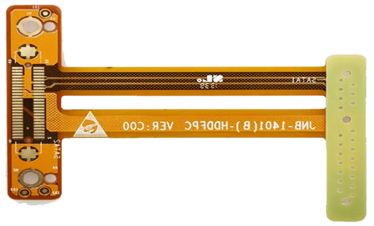
Flexible PCB
Flexible circuit boards are versatile circuit board that utilizes a flexible base material. The boards are offered in various layers. They could either be single layers or two layers. Flexible PCBs contain a number of circuits and components. Polyamide films, which are conductive, or polyetherether ketone, are the main components used in these PCBs.
Rigid PCB
This kind of PCB makes use of a solid material to make it. This keeps the board from twisting. It is impossible to stretch a stiff PCB as the material is solid. These boards have a number of intricate circuits around them. The primary component of rigid PCB boards is a sturdy substrate. The substrate gives the board strength and rigidity. A rigid PCB have multiple layers. The layers include the solder mask silkscreen copper, substrate, and solder mask.
It is essential to understand that rigid boards can be made up of various layers. It could be a single layer or multilayer. It is dependent on the application. But you can’t modify this kind of PCB once you manufacturing them.
The rigid circuit boards work well for applications such as control towers, the GPS system as well as scans using CAT. These boards are low in electronic noise and are also cost-effective. They are also able to endure the effects of vibrations. The computer motherboard is an excellent example of this type of board.
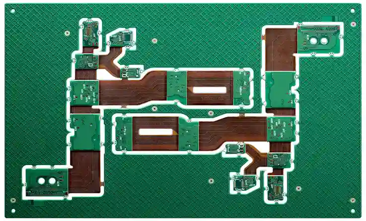
Rigid Flex PCB
A rigid-flex board blends the advantages of a flexible and rigid board. The PCB boards provide excellent flexibility. The majority of applications use these boards due to their characteristics. The flexible portion of this type of board makes it perfect for connecting board with rigid components. Flexible-flex designs are complicated because they are created in 3D.
The rigid-flex PCBs are lightweight and durable. These boards are perfect for applications such as consumer electronics, medical and aerospace.
PCBs With Different Types Based on Layers
PCB boards come in various kinds. Depending on the application, you will receive a different type. For the most complicated devices, Multi-layer PCBs are the best choice. The majority of simple applications require PCBs with a single layer.
Single Layer PCBs
As the name suggests, single layer PCB is a circuit board type that has only one layer of conducting material (usually copper) on one side, while the other side is used for attaching electronic components.
Consequently, a single-layer PCB consists of a substrate layer, a conductive metal layer, a protective solder mask, and silk-screen, which makes up a complete board with pads, vias, mounting holes, wires, components, connectors, filling, and electrical boundaries.
Single-layer PCBs form the basis of printed circuit board technology. They still have a major role to play in the electronic industry.
Double–Sided PCB
Through-hole technology by-hole technique introduces lead components through the holes already drilled in the circuit board. Surface mount technology places electronic components directly on the circuit board.
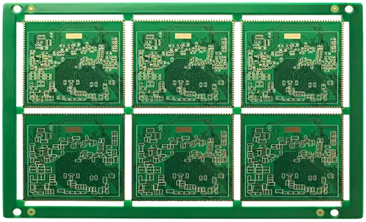
Multilayer PCBs
The multilayer PCB consists of double-sided boards that are stacked one on top of the other. The stack-ups typically have three boards with double sides. However, they can also contain more boards than are required for the project. But, an inconsistency of layers may cause warping or twisting when soldering is applied, so it is best to select an equal amount of layers.
Multilayer PCBs are made by laminating layers of core and prepreg material at high temperatures. As the conductors are completely covered with resin in this process, and the adhesive that holds the layers together is melted appropriately. Therefore, this process ensures that there is no trapped between layers for conductors. Materials used in multilayer PCB fabrication can range from basic epoxy glass to more sophisticated ceramics and Teflon materials.
Multilayer PCBs are used for computer systems, file servers, GPS technology, satellite devices, handheld devices, medical equipment, such as heart monitors, X-ray machines as well, cat scan technologies, nuclear detection systems as well as space probe equipment for transmission of signals, and many other high-tech gadgets.
Materials Used in the Design of PCBs
A variety of materials comprise the PCB. A dielectric substrate forms the primary part of PCB. It is able to be flexible or rigid.
FR4
This is an epoxy-based laminate that is reinforced by the glass. FR-4 includes a flame-resistant material and a woven glass cloth. It is a popular material used by engineers to make PCB manufacturing. The word “FR” simply refers to fire retardant. This material has excellent mechanical and electrical strength. FR-4 is a material with a strong tensile strength.
The majority of material FR-4 has bromine which is used to prevent the spread of flames. The material is able to withstand moisture. This is why it is perfect for some applications.
Flex
The majority of standard PCBs feature an aluminum or fiberglass base, and flex circuits’ cores are composed of an elastic polymer. Most flex PCB is made of the polyimide (PI) film for the substrate. The PI film doesn’t soften when heated. However, it remains flexible after it has been thermoset.
Ceramic
Also, a ceramic PCB is a printed circuit board that has ceramic as the base material. It is a highly thermally conductive material like aluminum nitride, alumina, and also beryllium oxide. It has a rapid impact on dispersing heat from hot spots and dispersing it throughout the entire surface.
Matel
Metal is the most commonly used material used in PCB fabrication. There are a few examples. Aluminum, iron, and copper are the most conductive layers of circuit boards. A majority of PCB boards are covered with copper. Metal allows the use of SMT for joining components. The material also has physical durability and strength.
It is vital to select the right material when it comes to PCB production. There are a variety of materials used in PCB production, and they all have advantages and disadvantages. Environmental aspects are crucial to be considered. Choose the best materials for your needs.
Where Can PCB Be Used
The printed circuit boards are perfect to be used in a variety of applications. In recent years, PCBs have gained a number of advantages, making them a preferred choice for the majority of modern technology applications. Circuit boards printed with circuits are utilized in the following fields:
LED
Circuit boards printed with circuitry provide the perfect base for various high-output LED solutions.The use of LEDs in lighting solutions across a variety of industries is rapidly growing. They’re admired for their low power usage and high efficiency, as well as their impressive lighting output. When connected to a PCB, LEDs are able to gain more flexibility. PCBs allow for a wider range of uses for LED lighting, particularly as display and indicator.
Consumer Electronics
This is another industry that makes use of PCBs, which are printed circuit boards. Computers, as well as phones, require using PCBs. The need for PCBs continues to grow when we integrate them into our devices. Smaller devices require smaller PCBs with the highest performance.
Tablets, radios, smartwatches and smartphones, as well as other devices, utilize PCBs. Computers also come with PCBs. These circuit boards are used in modern home appliances.
Computer
PCBs, also known as printed circuit boards, are made of fiberglass boards that have copper traces to connect resistors, transistors, and integrated circuits to create an integrated system.
An excellent example of a printed circuit board is the motherboard of a computer. Motherboards are the most extensive printed circuit boards found in desktop computers, connecting all other components.
In addition to connecting the memory and CPU in other systems, it also stores and facilitates communication among all the most crucial electronic components.
Telecommunication
In the telecom industry, PCB plays an important function. It is a perfect circuit board for consumer electronics. The sector employs a variety of PCBs due to the various kinds of equipment available. The industry of telecommunications is growing, and consequently, the usage of PCB is increasing.
Telecom equipment, such as telephone switching systems, LED displays modems, LED displays, and more requires circuit board prototypes. Since more and more information is transmitted, PCBs that are high-performance will become more useful for communications.
Automotive
The automobiles of today are increasingly dependent upon electronic parts in the current time. In the past, electronic circuits were typically utilized to switch on headlights and windshield wipers. Vehicles use electronic components for many other uses.
Modern automobiles benefit from the ever-changing electronic circuitry by incorporating PCBs in innovative applications. PCBs that work with high-frequency signals such as microwave, RF, or millimeter-wave frequencies are commonly employed in sensor-related applications that are becoming commonplace in cars. In reality, radar technology that was once restricted to military vehicles is now used in modern cars to aid cars in avoiding collisions, identifying blind spots, and adjusting to traffic conditions while the vehicle is in cruise control.
These modern systems provide improved road safety while giving drivers a more enjoyable driving experience. That’s the reason they are so common in modern motor vehicles. The companies that make these systems need to find and employ an increasing quantity of High-frequency circuits and related materials.
Medical
The advent of PCBs has significantly improved healthcare. PCBs are perfect for making medical electronic components. They are used in MRI machines as well as computers, radiation equipment and many others. The compact size of flexible and rigid boards allows for the development of smaller equipment.
These boards are found in hearing aids, implantable devices, and all cameras that are tiny. If you’re looking to decrease the size of complicated devices, rigid-flex boards are a great choice. These boards won’t require connectors or flexible cables. Connectors and flex cables occupy larger space in devices with complex layouts. PCBs can be found in the smallest of devices.
Industrial System
The majority of industrial machines that use heavy power make use of PCBs. In the field of electronic manufacturing, PCBs play an important role. PCBs have improved automation, information and efficiency. PCBs are the most efficient way to improve manufacturing.
PCBs made of heavy copper is used in cases where copper-based boards of one ounce won’t be used. The heavy copper boards are found on load testers and motor controllers, and many more.
Aerospace
The aerospace industry is another sector that depends on PCB. PCB circuit boards are used in products like flight control and flight management systems and many more. The smaller and more intricate boards are perfect for aerospace electronics. Flexible and rigid boards offer the ability to withstand and are durable. These boards can also be free of connectors, which makes them ideal for high-vibration environments.
Aerospace equipment requires the need for boards that stand up to extreme temperatures and vibrations. Boards made of aluminum can also be used in the aerospace industry. An electronic circuit board (ECB) is a key element in aerospace equipment.
Military
PCBs are an essential part of the majority of military equipment. They can withstand extreme shock, vibration, and heavy impacts. This is why they are the ideal option for these gadgets. PCBs are ideal for the manufacturing of military vehicles as well as modern weapons.
Military technology is now integrating computers to meet the highest requirements. In the military, the majority of devices are exposed to extreme temperatures. High Frequency PCBs are the most suitable choice for manufacturing these devices.
PCB Advantages and Disadvantages
The PCB is the term used to describe the circuit printed on board. It is an essential component of modern electronic equipment. The printed circuit board is comprised of an extensive array of active and passive components needed. The components are linked in a series of lines across the boards. It is absolutely possible to create huge circuits on tiny printed circuit boards, thanks to the use of tiny electronic components. Let’s take a deeper understanding of the advantages and drawbacks of the printed circuit board so that we can learn what it is all about.
The Advantages of PCB
Low Cost: PCBs offer low costs of production for large-scale production.
Low Noise: A PCB gives less electronic noise. If it’s not properly laid out, the noise can negatively affect the efficiency that the circuit is able to provide.
There is no chance of short Circuits: One of the benefits using PCB since that the connections for design are via copper tracks, and there is no risk of short or loose connections.
More robust: Utilizing a PCB to build your design concepts is typically more beneficial as it extends the lifespan of your design by not having to wire copper with physical wires.
Immune To Moving: The structure and design of a PCB allow it to be naturally immune from vibrations and movement. Therefore, regardless of how the PCB moves , it will ensure that all components remain in place.
Reliability: PCBs that are used for time-intensive tasks can be more reliable since they are less susceptible to electrical problems and are easier to troubleshoot in case of design-related issues.
Easy To Check & Repair: PCBs allow you to identify and fix problems within a short amount of time. Electronic components, along with their respective poles, are constructed and identified onto the PCB. If there is a problem, it’s simple to find and make replacements.
It saves Time: The standard method of connecting circuits takes a long to connect the components. The printed circuit board is able to take less time to put together the circuit. It is due to this property that PCBs are very suitable for tasks that require a quick response time.
Compact Size: PCBs have the advantage of being able to be inserted into areas where the clearance is limited. They are connected by using copper tracks instead of regular wires. This means it can be connected to thousands of components without having to worry about the dimensions of the board.
PCB’s Disadvantages
● Solder bridge.
● Thermal shock.
● Reduced or plugged.
● It’s a lead-based product.
● Uneven PCB surfaces finish.
● Not recommended for fine-pitch.
● It could be used to create a particular circuit.
● We are not able to be changed it after printing.
● It’s not easy to fix after the damage has occurred.
● Redesigning is necessary for a particular kind of operation.
● The process of etching generates chemical compounds that have a negative impact on the environment.
Find a Manufacturer for Your PCB Application
PCB is an adaptable and flexible solution that can be used for a variety of applications across many industries. A reputable and skilled manufacturer can provide create a cost-effective and easily manufacturable PCB solution for any application to meet the needs of any industry. If you’re searching for an experienced PCB solution provider, JarnisTech can assist.
We provide top PCB solutions for businesses all over the globe. We collaborate with our clients to design PCBs that surpass their expectations and meet every need while providing complete knowledge, unparalleled quality assurance, and efficient production methods. If you decide to collaborate with JarnisTech and you’re partnering with a service provider who is committed to your satisfaction and to the highest quality assurance standards. Our PCB board manufacturing and assembly services follow IPC Class 3, RoHS, and ISO 9001:2008 certification standards, and we continue to seek out the latest certifications to ensure that we are providing the best services possible. Our main objective is to help you reduce time and costs so that you do not have to think over PCB production and instead focus only on PCB designs and the development of your product.
No matter what kind of PCB your business requires, we will be able to provide it. Single or double-sided, SMT, through-hole or mixed assembly, we’ll design it at the lowest cost. Get in touch with us for more details regarding PCB design and application, and click the next buttons to request a quote quickly!