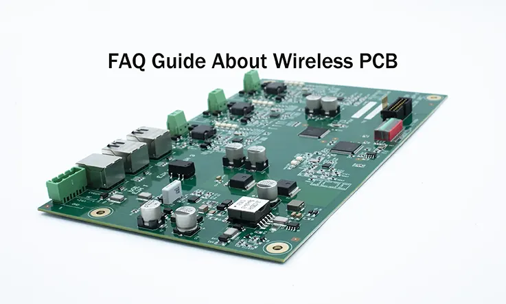
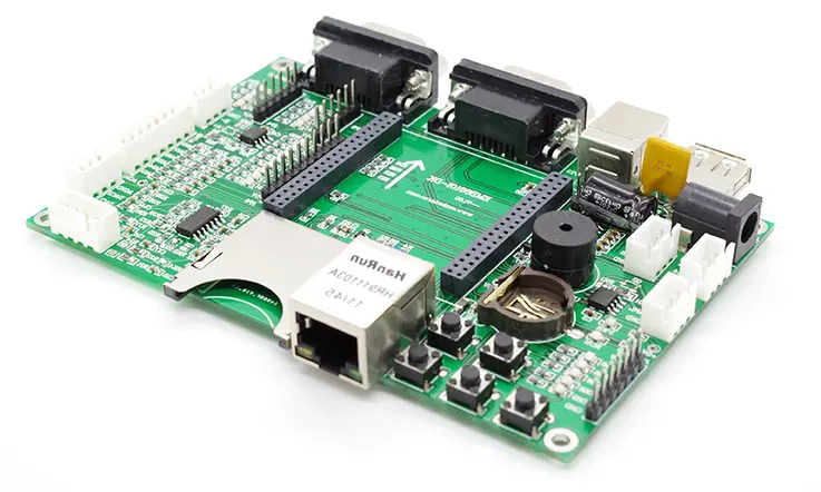
Wireless PCBs are integral to various industries like telecommunications, smart infrastructure, and consumer electronics. They are designed to support high-frequency signals, antenna integration, and electromagnetic compliance. This guide will help you understand the types of wireless PCBs, design influences, materials, and assembly processes that impact performance.
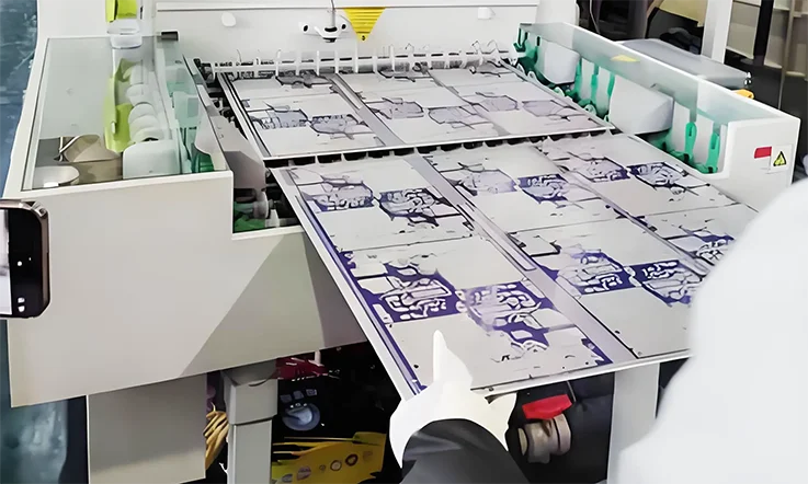
The fabrication process involves steps like etching, lamination, and laser drilling, with materials such as PTFE and high-speed laminates used to ensure signal integrity. Many manufacturers offer services from schematic design to final layout, often including RF simulation and support for custom designs.
SMT is commonly used for smaller RF modules, while DIP suits larger boards. After assembly, testing ensures the functionality and quality of the final product. For more complex applications like 5G or IoT, custom stackups and routing are employed to meet specific demands.
This guide provides detailed insights into wireless PCB design and manufacturing for professionals looking to optimize their projects.
What is a Wireless PCB and Why Is It Essential?
In today’s connected world, wireless PCBs (Printed Circuit Boards) form the backbone of devices that communicate wirelessly. These boards are specifically engineered to handle signals in high-frequency ranges, enabling smooth and reliable data transmission across various devices without physical connections.
Definition and Core Functions of Wireless PCBs
A wireless PCB is a specialized circuit board that supports wireless communication standards such as Wi-Fi, Bluetooth, and RF (Radio Frequency). Unlike traditional PCBs, these wireless boards are designed to integrate critical components such as antennas, transceivers, and filters that facilitate seamless wireless communication.
Main Functions-
●Signal Transmission: Enables high-frequency signal transmission with minimal loss.
●Impedance Matching: Ensures that signal pathways match the impedance of connected loads to ensure smooth power transfer and reduce signal distortion.
●Electromagnetic Compatibility (EMC): Minimizes electromagnetic interference, ensuring the board works reliably in various settings.
Example: Consider a wireless Bluetooth mouse. The wireless PCB inside the device transmits user inputs via Bluetooth to the computer, ensuring smooth and responsive communication without the need for physical cables.
Role of Wireless PCB Design in Modern Electronics
The design of a wireless PCB directly affects how a device functions by guiding the communication between components efficiently. Several design elements must be considered to support stable and reliable performance, including signal routing, material selection, antenna placement, and impedance control.
●Material Selection: Materials such as Rogers or FR-4 are selected for their low dielectric constant, which allows reliable high-frequency communication.
●Layer Stack-Up: Multi-layer designs separate signal layers to reduce the risk of interference, providing a clean signal path.
●Component Placement: Efficient placement of components reduces signal path lengths and avoids interference, promoting smooth data transfer.
Example: In the case of a smartphone, a wireless PCB facilitates communication between Bluetooth, Wi-Fi, and other wireless modules. The design ensures that signals do not interfere, maintaining stable connectivity during use.
Industries Served by Top Wireless PCB Manufacturers
Wireless PCBs are used across a broad spectrum of industries, each with unique demands and requirements:
| Industry | Applications | Wireless PCB Requirements |
| Medical Devices | Wearable health monitors, implantable devices | Miniaturized designs, durability, high reliability |
| Consumer Electronics | Smartphones, wireless earbuds, gaming consoles | Compact design, efficient high-frequency handling |
| Aerospace and Defense | Navigation systems, communication devices | Reliability in extreme conditions, signal integrity |
| Telecommunications | Routers, cellular towers, modems | Signal integrity, scalability, high performance |
| Automotive | Keyless entry, wireless charging systems | EMC compliance, ruggedness in tough environments |
Example: In the automotive industry, wireless PCBs are integral to systems like keyless entry and wireless charging, providing both functionality and convenience in modern vehicles.
What Are the Types of Wireless PCBs Available Today?
Wireless PCBs are in high demand across telecommunications, industrial control, medical monitoring, and aerospace sectors. Each area requires its own approach to signal transmission, structural layout, and space limitations. Industry experts and production teams tackle these demands by offering a range of board types, each designed for particular application needs. This section outlines the primary classes of wireless PCBs in today’s electronic product development and their performance characteristics.
Single-Sided vs. Multilayer Wireless PCBs
Choosing the appropriate PCB configuration often starts with assessing the circuit’s complexity, component density, and routing needs. Two widely used categories in wireless PCB design are single-sided and multilayer formats.
Single-Sided Wireless PCBs-
These boards have a single layer of conductive copper and are commonly built from FR4, CEM-1, or similar substrates. This configuration often suits devices with minimal circuitry or basic wireless modules. Its straightforward layout and assembly process support efficient production, particularly for consumer-grade items or prototype runs.
Multilayer Wireless PCBs-
When signal density increases or controlled impedance is required, multilayer boards offer a more scalable approach. These PCBs integrate multiple conductive layers separated by dielectric material and allow for complex routing between components. Wireless PCB fabrication techniques such as sequential lamination and via-in-pad processing are common for multilayer applications.
Design Factors in Wireless PCB Fabrication-
Human’s engineers take into account material dielectric constant, copper thickness, signal loss, and thermal performance during the design process. Multilayer wireless PCB manufacturing also involves blind and buried vias to preserve board real estate and enhance signal flow efficiency.
Flexible and Rigid-Flex Wireless PCB Configurations
Modern device architecture increasingly relies on form factor versatility and reduced interconnect complexity. Flexible and rigid-flex wireless PCBs are widely used when circuit boards must conform to non-linear geometries or dynamic movements.
Flexible Wireless PCBs-
Built on substrates like polyimide or LCP (liquid crystal polymer), these PCBs allow for bending and shaping. Their wireless connectivity components are typically surface-mounted, requiring precise alignment and soldering during wireless PCB assembly. These configurations are often found in wearables, implantable medical electronics, and compact handheld devices.
Rigid-Flex Wireless PCBs-
Combining rigid sections for structural stability with flexible layers for inter-module connections, rigid-flex layouts remove the need for external cables and connectors. This approach is commonly used to lower mechanical failure points and shrink overall device size.
Process Notes from Wireless PCB Manufacturing Services-
Rigid-flex fabrication requires accurate material alignment, controlled impedance zones, and specialized lamination. During wireless PCB assembly, careful thermal profiling ensures integrity at the interface between rigid and flexible regions.
HDI, RF, and Bluetooth-Enabled PCB Types
Specific applications require unique characteristics in performance, density, or signal behavior. For these cases, wireless PCB design expands into advanced categories such as HDI, RF, and integrated Bluetooth layouts.
HDI Wireless PCBs (High-Density Interconnect)-
These PCBs feature microvias, ultra-thin dielectric layers, and stacked vias for compact, high-performance layouts. Production facilities employ laser drilling and sequential build-up (SBU) techniques to achieve greater density and tighter tolerances. HDI layouts are common in miniaturized communication devices and high-frequency systems.
RF Wireless PCBs-
Used for transmitting and receiving high-frequency signals, RF wireless PCBs are fabricated with low-loss materials such as PTFE or ceramic-filled laminates. Wireless PCB fabrication includes impedance matching, signal shielding, and simulation testing at frequencies ranging from MHz to GHz.
Bluetooth Wireless PCBs-
These are designed to support short-range wireless protocols, typically embedding certified Bluetooth modules into the board layout. Engineers working on wireless PCB design must focus on antenna placement, EMI control, and compliance with international wireless transmission standards. Assembly processes follow strict guidelines for solder joint inspection and layout integrity.
How Does Wireless PCB Design Impact Performance?
Wireless PCB design influences how signal quality, stability, and electromagnetic behavior align with product specifications across industries such as telecommunications, consumer electronics, and defense. With the increasing use of high-frequency signals, integration of antennas, and compact form factors, the performance of a wireless-enabled circuit board relies on a wide range of design parameters. Each stage of design and fabrication requires attention to layout geometry, materials, and signal flow.
High-Frequency Layout Considerations for RF Signals
For wireless PCBs that transmit or receive RF signals, the physical layout must manage factors like impedance, signal loss, and trace coupling. Common layout techniques aim to stabilize frequency behavior and minimize disruptions during operation:
●Controlled Impedance Routing helps maintain consistent transmission by aligning trace width, copper thickness, and dielectric constants.
●Short Trace Paths help lower signal delay and phase errors, benefitting Bluetooth-enabled and RF-based PCBs.
●Layered Ground Planes provide a return path that reduces signal radiation and promotes cleaner transitions at high speed.
Wireless PCB design experts also account for component spacing to reduce parasitic capacitance, while wireless PCB manufacturers often offer guidelines for stack-up configurations tailored for specific frequency targets.
Antenna Placement and EMI Shielding Strategies
Antenna efficiency in wireless PCBs depends on isolation from noise, placement relative to ground planes, and physical proximity to active components. During the wireless PCB assembly process, board shape and material finish also influence how radiation patterns behave.
Typical strategies include:
●Edge Positioning: Antennas are placed at the perimeter of the PCB to avoid interference from dense routing zones.
●EMI Shielding Layouts: Ground fences, via stitching, and dedicated shielding layers can contain electromagnetic noise.
●Matching Networks: Passive component tuning matches antenna impedance to system impedance, enhancing transmission accuracy.
Material Compatibility During PCB Design Stages
The electrical and mechanical properties of base materials shape how RF and wireless signals behave. Each material option presents trade-offs between signal retention, manufacturability, and thermal stability during reflow or assembly.
When selecting materials for wireless PCB fabrication, we usually consider:
●Dielectric Constant (Dk): This parameter influences trace dimensioning and is used in impedance calculations. Lower values typically offer more predictable signal paths.
●Dissipation Factor (Df): Affects how much signal is lost as heat across the board—lower values are preferred for maintaining signal integrity.
●Thermal Expansion: A mismatch in expansion between copper layers and substrate may cause delamination or stress during soldering.
Wireless PCB materials such as PTFE composites, ceramic-filled hydrocarbon laminates, and high-Tg FR-4 alternatives are frequently used based on the application’s thermal and frequency requirements.
What Materials Are Used in Wireless PCB Manufacturing?
In the production of wireless PCBs, choosing the right materials is a determining factor for the efficiency, performance, and durability of the final product. The materials used in wireless PCB manufacturing not only impact the electrical properties of the board but also influence other factors such as production costs, ease of assembly, and overall reliability. Below is an exploration of the commonly used materials in wireless PCB manufacturing.
PTFE, Rogers, and High-Speed Dielectric Laminates
For high-frequency applications like RF (Radio Frequency), choosing the right dielectric material makes a noticeable difference. PTFE (Polytetrafluoroethylene) and Rogers laminates are common choices, thanks to their low signal loss and stable performance across a wide range of frequencies.
PTFE-
PTFE is known for its low signal loss and high thermal resistance. These properties make it suitable for high-frequency applications such as satellite communications, radar systems, and high-speed digital circuits. PTFE ensures that the signal transmission remains clear even over long distances and high frequencies, without significant degradation.
Rogers-
Rogers materials, designed for high-frequency applications, provide a range of dielectric laminates that maintain signal integrity across multiple frequencies. Some commonly used Rogers laminates are:
| Material | Frequency Range | Applications |
| RO4000 Series | Up to 20 GHz | Telecommunications, Wi-Fi |
| RO3003 Series | Up to 50 GHz | Automotive, 5G networks |
| RO4350B | Up to 6 GHz | Consumer electronics, RF systems |
Rogers laminates have been optimized to ensure that signal strength is maintained even under varying temperature and environmental conditions, ensuring that the wireless device performs consistently.
Conductive Layers and Copper Weight Guidelines
The copper layers used in a wireless PCB play a core role in determining the electrical performance and durability of the board. The thickness of the copper and the weight of the copper in the PCB affects parameters such as current handling capacity, heat dissipation, and signal integrity.
Here are some general guidelines for selecting copper weight in PCB manufacturing:
●Light Copper (1 oz/ft²): Common in low-power devices, providing adequate conductivity for basic wireless applications.
●Medium Copper (2 oz/ft²): Often used for mid-range RF applications, where more current handling is needed.
●Heavy Copper (3 oz/ft² or more): Typically found in high-power applications that demand improved heat dissipation and increased current capacity to support overall system operation.
| Copper Weight | Application Area | Typical Frequency Range |
| 1 oz/ft² | Basic wireless devices | Up to 1 GHz |
| 2 oz/ft² | Mid-range RF applications | 1 GHz – 6 GHz |
| 3 oz/ft² | High-power RF systems | 6 GHz and above |
The copper weight selected will depend on the specific needs of the wireless PCB, such as power requirements and signal transmission frequency.
Thermal Stability and Signal Loss Considerations
Thermal stability and signal loss are closely linked in wireless PCB manufacturing. The material used must perform consistently even under different temperature conditions and maintain a strong signal without excessive loss.
Thermal Stability-
High-performance wireless PCBs are typically made from high-Tg FR4 or ceramic-filled composites. These materials offer stability under thermal stress and can withstand the heat generated during the soldering process without affecting the structure of the PCB. This ensures that the device continues to function as expected under varying environmental conditions.
Signal Loss-
Signal loss can be influenced by the dissipation factor (Df) of the material. A higher Df leads to more signal degradation, which can affect the performance of wireless systems. Materials like Rogers RO3003 and PTFE offer low Df values, which minimize signal loss and ensure clearer and more efficient signal transmission.
Here is a breakdown of common PCB materials and their respective electrical characteristics:
| Material | Dielectric Constant (Dk) | Dissipation Factor (Df) | Typical Applications |
| RO3003 | 3.0 | 0.003 | 5G, high-speed RF |
| PTFE | 2.2 | 0.0003 | Satellite systems |
| FR4 (High Tg) | 4.2 | 0.02 | General consumer devices |
Choosing a material with a low Df helps lower signal loss, especially in high-speed or high-frequency applications.
What Services Do Wireless PCB Manufacturers Provide?
Wireless PCB manufacturers offer a wide range of services designed to support the creation, testing, and production of printed circuit boards used in wireless communication devices. These services encompass every phase of development, from the initial design to the final product, and are customized to meet the specific requirements of various wireless applications. Let’s take a closer look at the core services that these manufacturers offer.
From Schematic Design to Final PCB Layout
Creating a functional and reliable wireless PCB begins with detailed schematic design, which defines the electrical connections and functional layout of the circuit. Wireless PCB manufacturers assist in the creation of these schematic designs, ensuring all design parameters, including frequency, signal integrity, and power efficiency, are met. After the schematic is finalized, the next step is converting it into a physical layout.
●Schematic Design: This process defines the circuit’s functionality and ensures all electrical connections are correct. The schematic design helps ensure that the selected components will deliver the required performance for wireless communication.
●Final PCB Layout: The layout phase involves arranging the components on the board and routing the connections. This step requires attention to detail, such as trace widths and component placements, to optimize performance and reduce potential issues related to signal loss or interference.
During this stage, PCB manufacturers often use simulation tools to predict the performance of the design before the physical production starts. This helps identify potential problems early on, minimizing the risk of costly revisions during later stages.
RF Simulation and Signal Optimization Services
RF signals used in wireless communication devices require careful handling to maintain signal strength and integrity. Without proper attention, signal degradation or interference can significantly affect the performance of the device. Wireless PCB manufacturers offer RF simulation services to ensure that the final design meets the required standards for signal quality.
Signal Integrity-
Some of manufacturers use RF simulations to test how the PCB will handle various frequencies. The goal is to maintain a high level of signal integrity, which is especially important for high-frequency applications like Bluetooth, Wi-Fi, and 5G. The simulation tools analyze the PCB layout and predict any potential issues related to signal loss or distortion.
Electromagnetic Interference (EMI) Mitigation-
Another major aspect of RF simulation involves controlling electromagnetic interference (EMI).Poor management of EMI can lead to performance issues or disrupt nearby electronic devices. Manufacturers use simulation tools to assess and optimize the design, ensuring that the PCB minimizes EMI and maintains strong signal quality in diverse operating environments.
These simulation and signal optimization services help ensure wireless devices perform optimally, even in challenging environments with higher levels of interference.
PCB Supplier Support for Custom Projects
Custom wireless projects receive dedicated assistance that aligns with each design’s exact requirements. From choosing advanced substrates and defining multilayer arrangements to sourcing niche components, these services ensure every PCB adheres to its intended specifications.
●Material Selection: Custom wireless PCBs often require materials that cater to high-frequency signals, such as PTFE, Rogers, or specialized FR4 variants. Manufacturers assist in selecting the appropriate materials to ensure performance and signal integrity.
●Layer Configurations: Custom PCBs may require multiple layers or specific stacking arrangements to meet space constraints and performance demands. Manufacturers offer configurations that fit the particular needs of the project, ensuring the PCB performs as expected.
●Prototyping Services: Before proceeding with full-scale production, manufacturers offer prototyping services to test the design in real-world conditions. Prototypes allow designers to verify the performance of the wireless PCB and make adjustments before committing to large production runs.
These support services ensure that each custom wireless PCB meets the specific performance requirements, avoiding unnecessary delays and ensuring a high-quality final product.
How Is a Wireless PCB Fabricated from Start to Finish?
The fabrication process of a wireless PCB involves several specialized stages, each directly impacting the performance of the final product. For wireless applications, ensuring that each phase is executed with precision is a foundational element in achieving high-quality signal transmission. The journey of making a wireless PCB begins with design and continues through to final assembly and inspection. In this section, we will walk through the steps, providing a clear view of how a reliable wireless PCB is manufactured from the ground up.
Key Fabrication Steps for RF-Grade PCBs
The manufacturing of RF-grade PCBs includes several steps that require high precision to ensure the final product supports high-frequency and high-speed signal transmission. The main steps include design, material selection, etching, lamination, and soldering:
1.Design and Schematic Creation: Every wireless PCB manufacturing process starts with designing and creating a schematic. During the design phase, parameters such as frequency and impedance need to be considered carefully to ensure the board supports the required signal transmission characteristics.
2.Material Selection: Choosing the right PCB material is fundamental. For RF-grade PCBs, high-frequency materials like PTFE and Rogers are often selected because they provide minimal signal loss for high-speed transmissions.
3.Lamination and Etching: After material selection, the PCB enters the lamination stage, where multiple layers of material are fused together using heat and pressure. Afterward, the board goes through an etching process to precisely form the circuit pathways and minimize signal interference.
4.Drilling and Plating: Drilling is essential to create vias, which connect the different layers of the PCB. Plating ensures a reliable electrical connection through these vias.
These steps help ensure that RF-grade PCBs perform well in wireless communication environments, minimizing signal loss or distortion.
Etching, Lamination, and Laser Drilling Explained
Etching, lamination, and laser drilling are main steps in the fabrication of wireless PCBs. Each of these stages plays a role in shaping the precision and performance of the final product.
1.Etching: Etching removes excess copper from the PCB and defines the exact circuit pathways. In wireless applications, this step demands high precision, since small deviations may cause signal loss or reduced performance.
2.Lamination: During lamination, PCB layers bond under heat and pressure. High-grade laminates like Rogers 4003C are chosen for their low-loss properties at high frequencies.
3.Laser Drilling:Laser drilling creates vias that connect the PCB’s multiple layers. This technology produces precise holes, supporting high-density interconnect (HDI) layouts.
These steps help ensure the PCB can handle electrical and thermal loads, maintaining reliability over time, and is suited for high-frequency signal transmission.
Final Surface Finish and Quality Inspection
After the basic fabrication of the PCB is completed, surface finishing is the final step. Proper surface treatment not only enhances the PCB’s durability but also ensures excellent solderability. Common surface treatments include:
●Gold Plating (ENIG): Provides excellent solderability and corrosion resistance, making it suitable for high-frequency applications.
●OSP (Organic Solderability Preservative): Often used for cost-sensitive projects, though it might not offer the same durability as gold plating in long-term use.
●HASL (Hot Air Solder Leveling): Commonly used for standard PCBs but is less suitable for high-frequency wireless applications due to its rough surface.
After surface finishing, the PCB moves to the final inspection phase. This includes:
●Electrical Testing: Verifying that the circuits work as intended and meet the performance requirements for wireless applications.
●Visual Inspection: Checking for physical defects such as cracks or misalignment.
●Thermal Cycling Test: Ensuring the PCB can withstand temperature variations that might occur during both production and operation.
The goal of these inspections is to confirm the reliability and long-term stability of the wireless PCB.
How Are Wireless PCBs Assembled with SMT & DIP?
The assembly process of wireless printed circuit boards demands precise coordination between layout planning and component integration. Surface Mount Technology (SMT) is generally applied to compact, high-frequency modules, while Dual In-line Package (DIP) techniques support larger, through-hole components. Each step contributes to electrical consistency, thermal stability, and structural alignment.
SMT Processes for RF Components and Modules
SMT enables dense component placement, particularly useful for high-frequency wireless designs where impedance control and signal routing precision are mandatory.
●Accurate component placement: Automated pick-and-place machines install passive and active RF parts on solder-pasted pads.
●Controlled reflow soldering: A temperature-controlled profile ensures solder melts uniformly and solidifies without thermal shock.
●Stencil design alignment: Proper aperture size and layout reduce solder bridging and optimize wetting on fine-pitch RF leads.
●Voiding control under ground pads: For QFN and LGA packages, vacuum reflow or via-in-pad techniques help minimize signal disruption from voids.
These steps ensure the RF signal path maintains consistency and minimizes electromagnetic reflection or attenuation.
SMT Process Parameters-
| Parameter | Typical Target | Notes |
| Pick-and-Place Accuracy | ±25 µm | Ensures correct placement of RF modules |
| Reflow Profile Peak Temperature | 245–250 °C | Melts solder uniformly without damaging substrates |
| Solder Paste Volume Variation | ±10% | Controlled via stencil aperture design |
| Void Percentage Under QFN Pads | <10% | Measured via X-ray inspection |
DIP Techniques for Larger Wireless PCB Boards
DIP assembly supports through-hole components that may require added mechanical strength, voltage isolation, or thermal dissipation.
●Preforming of leads: Leads are cut and shaped before insertion to match the board’s drilled hole dimensions.
●Wave soldering operation: The board is passed over a molten solder wave that forms uniform joints across the entire bottom surface.
●Use of alignment jigs: Fixtures help stabilize heavy or multi-lead components during insertion and soldering phases.
Through-hole methods are often selected for RF power amplifiers, antenna connectors, and large-value inductors.
DIP Process Parameters-
| Parameter | Typical Target | Notes |
| Lead Diameter Tolerance | ±0.05 mm | Matches hole diameter for reliable solder joints |
| Wave Solder Temperature | 250–260 °C | Provides good wetting without overheating components |
| Conveyor Speed | 1.0–1.5 m/min | Balances throughput and solder joint quality |
| Fixture Alignment Accuracy | ±0.1 mm | Ensures proper seating of heavy or large components |
Post-Assembly Testing and Functional Validation
After assembly, multiple verification layers are applied to ensure the assembled PCB matches the design intent and maintains operational consistency under various conditions.
●Automated Optical Inspection (AOI): Cameras and recognition algorithms detect offset, polarity reversal, or tombstoning.
●In-Circuit Testing (ICT): Verifies resistance, capacitance, and continuity values directly through contact probes.
●RF performance checks: Measurements such as S-parameters, insertion loss, and radiation patterns validate high-frequency behavior.
●Environmental stress testing: Thermal cycling and humidity exposure simulate long-term field use.
Testing Parameters-
| Test Method | Typical Range / Spec | Purpose |
| AOI Resolution | 10–20 µm | Detects misalignment and solder defects |
| ICT Test Points | >98% coverage | Confirms correct electrical connections |
| VNA Frequency Range | 100 MHz–40 GHz | Measures S-parameters and insertion loss |
| Thermal Cycle | −40 °C to +85 °C, 500 cycles | Assesses durability under temperature swings |
How Do Wireless PCB Manufacturing Services Support Innovation?
Modern wireless systems—from autonomous drones to machine-to-machine IoT networks—demand printed circuit boards that meet high-frequency, low-latency, and multi-layer routing requirements. Manufacturers in this space offer tailored workflows, adaptive tooling, and engineering support that align with emerging tech demands. These services help developers shift from early concepts to tested, manufacturable hardware without compromising design precision or RF reliability.
From enabling high-frequency handling to supporting iterative design cycles and rapid production, wireless PCB service providers act as technical collaborators across various applications. The following sections describe how this support unfolds through each phase of innovation.
Enabling 5G, IoT, and AI-Driven Devices
Designs involving high-frequency signals—particularly above 3 GHz—require the use of low-Dk, low-loss dielectric substrates, and extremely tight process control. Manufacturers that serve this segment frequently integrate PTFE, ceramic-filled laminates, or hydrocarbon-based cores, all of which maintain stable dielectric performance across wide temperature and humidity ranges.
Multilayer boards used in AI devices often include embedded antennas, controlled-impedance transmission lines, and high-density interconnects (HDI). These boards rely on simulation-backed layout design, where tools such as Ansys HFSS or Keysight ADS are used to validate signal propagation and return loss before fabrication begins. For example, a 6-layer board for a 5G module might feature microstrip and stripline routing across different planes to minimize radiation and crosstalk.
Additionally, manufacturers may provide impedance coupon testing and S-parameter validation to support compliance in mmWave applications, such as automotive radar or edge AI sensors.
Scalable Production for Startups and OEMs
Manufacturers support innovation not only through technical capability but also through production scalability. Early-stage development may require just 5–50 units for evaluation, while full-scale deployment may call for tens of thousands of boards monthly. To manage this variation, flexible production models are implemented.
For instance, manufacturers often provide multi-panel layout optimization and serialized tracking using manufacturing execution systems (MES), which are especially relevant in medical and industrial sectors. This enables consistency in both prototype and mass production, reducing variability between lots.
Engineering support teams often assist with component lifecycle review and alternate sourcing strategies. This is particularly helpful when dealing with supply chain disruptions or when transitioning a prototype BOM to one suited for large-scale, RoHS-compliant builds.
Smart Prototyping with Rapid Turnaround
Prototyping services now extend far beyond simple fabrication. Many providers offer integrated DFM (Design for Manufacturability) checks, real-time layout adjustments, and RF simulation services in-house. This streamlines the process of converting Gerber files into functioning PCBs, often with turnaround times of 3 to 7 working days for multilayer RF designs.
Technologies such as laser direct imaging (LDI), sequential lamination, and via-in-pad structures allow for the compact layouts often required in IoT edge modules and wearable devices. Post-processing includes X-ray inspection, AOI (automated optical inspection), and functional testing based on customer-supplied test jigs or firmware.
These capabilities support rapid iteration, which is especially useful in environments where regulatory testing or field validation must begin early in the product development cycle.
What Makes a Wireless PCB Design Truly Custom?
Custom wireless PCB design refers to more than just meeting size or frequency constraints—it’s about matching application-specific mechanical, RF, and manufacturing needs in a way that general-purpose boards simply cannot support. These tailored designs often incorporate advanced materials, non-standard stackups, and features like integrated antennas or specialized routing methods. The process requires close coordination between designers, fabrication engineers, and end-use requirements, particularly when the device integrates wireless protocols such as BLE, Wi-Fi 6, Zigbee, or mmWave 5G.
Below, we explore the technical decisions that shape a fully customized wireless PCB.
Integrating Embedded Antennas and Custom Form Factors
When wireless communication is built into a device, antenna integration becomes a primary design constraint. Instead of relying on external antenna modules, embedded designs often use structures such as meandered lines, IFA (inverted-F antennas), or fractal geometries within the PCB itself.
●These designs demand consistent impedance and careful isolation between radiating elements and active components. Manufacturers often use specific substrate materials like Rogers 4350B or Taconic RF-35 to preserve signal quality.
●Non-rectangular board shapes may be required to conform to wearable devices, compact industrial enclosures, or medical-grade equipment housings. In such cases, laser routing and depth-controlled milling are applied to achieve the required dimensions without affecting signal paths.
●Simulation tools like CST Microwave Studio or HFSS are used to validate antenna performance prior to production.
For example, a GPS module integrated into a curved smartwatch enclosure might require an embedded ceramic chip antenna placed on a ground-cleared region of the board with a direct feed from a matching network—custom-tuned to the wrist’s reflective body characteristics.
DFM (Design for Manufacturability) and Cost Reduction
While design goals often focus on RF performance, manufacturability must also be addressed. DFM practices are applied to minimize fabrication issues, reduce lead time, and control costs.
●Manufacturing tolerances must align with trace width/spacing, via diameter, and copper-to-edge clearance values defined by the fabrication house.
●Boards are often evaluated using Gerber checks, IPC-2221 guidelines, and stackup verification to avoid warpage, poor lamination, or unexpected layer shift.
●Cost drivers such as layer count, HDI via usage, and finish type (ENIG vs. ENEPIG) are analyzed and optimized in collaboration with the supplier.
For instance, moving from a 10-layer stackup with via-in-pad and laser vias to an 8-layer alternative with staggered microvias and standard press-fit connectors may reduce production costs by up to 25%, depending on volume and board complexity.
Customer-Specific PCB Stackup and Routing
Tailored stackups allow us to control impedance, reduce EMI, and support specific signaling architectures, especially in RF systems with mixed analog/digital paths. Stackups are usually determined by a mix of simulation outcomes and material performance.
●Common wireless applications may require buried shielding layers, isolated ground planes, and differential pair routing for high-speed interfaces like USB 3.0 or PCIe.
●Trace width and spacing are selected based on target impedance—often 50 ohms for single-ended RF and 100 ohms for differential signals.
●Routing constraints are also influenced by connector placement, antenna tuning circuits, and component clearance rules defined by enclosure dimensions.
Example: A 6-layer custom PCB used in a drone telemetry system might reserve layer 2 for RF ground, layer 3 for signal distribution, and implement cavity-backed structures for antenna modules on the top layer. This level of customization supports low loss transmission and optimized phase alignment across communication channels.
Wireless PCB Custom Design Parameters: A Comparison Table
| Parameter | Typical Range / Value | Impact on Design |
| Substrate Material | FR4, Rogers 4350B, Megtron6, Taconic | RF stability, loss tangent, thermal resistance |
| Trace Width Tolerance | ±10% or tighter | Consistent impedance for RF signal lines |
| Antenna Type | IFA, chip antenna, patch, PIFA | Affects radiation pattern and board layout |
| Board Thickness | 0.8 mm to 2.4 mm | Mechanical stiffness, layer configuration options |
| Layer Count | 4 to 12 layers | RF shielding, ground isolation, routing flexibility |
| Minimum Via Diameter | 0.1 mm (laser), 0.2 mm (mechanical) | Affects density and component placement |
| Common Routing Techniques | Microstrip, Stripline, Co-planar Waveguide | Controlled impedance and signal confinement |
FAQs about wireless PCBs
1.What are the benefits of flexible PCBs in wireless applications?
Flexible PCBs allow for adaptable designs in space-constrained or bendable devices, like wearables, reducing weight and size.
2.How do RF circuit simulations assist in wireless PCB design?
RF simulations optimize high-frequency circuit performance by predicting signal behavior and minimizing loss and interference.
3.What is the role of vias in wireless PCB design?
Vias, such as microvias or buried vias, optimize signal flow, reduce board size, and aid in heat dissipation.
4.What are typical size constraints for wireless PCBs?
Wireless PCBs are often compact, with size determined by component density, antenna placement, and multi-layer routing.
5.How do manufacturers address electromagnetic interference (EMI)?
EMI is minimized through shielding, strategic component placement, and ground plane designs to maintain signal quality.
Related Posts:
1. Exceptional Manufacturer of Antenna PCBs
2. JarnisTech – High Quality Bluetooth PCB Manufacturer
4. Why Carrier PCB in Telecommunication Is So Useful?
5. What Is GPS PCB and How to Use GPS Integration into PCB?
6.The Evolution of 5G PCB Technology: Transforming the Telecommunication Industry