
If you are interested in delving deeper into the intricacies of the 6-layer PCB stack up, you have arrived at the right destination. Multi-layer boards play a pivotal role in circuit and product designs, making it imperative to comprehend their operational principles to ensure successful product development.
In this enlightening blog post, we will elucidate the concept of a 6-layer PCB stack up, highlighting its indispensability and offering valuable insights into constructing a highly functional board.
We understand that the complexity associated with multi-layered boards can be daunting. However, our aim is to equip you with the necessary knowledge and expert advice, empowering you to tackle your most challenging design endeavors with confidence.
What is a 6 Layer PCB Stackup?
A 6-layer PCB typically comprises six distinct layers of conductive material, with two signal layers sandwiched between the four routing layers. PCB manufacturers strategically position these signal layers between the planes. This stackup configuration consists of two surface layers and two buried layers, with the remaining layers serving as internal routing layers.
This design approach offers several benefits, including enhanced Electromagnetic Interference (EMI) performance and improved signal routing capabilities. The buried layers are responsible for directing high-speed signals, while the surface layers handle low-speed signals. Achieving the optimal arrangement of insulating and copper layers is critical in a 6-layer PCB stackup.
The key layers in a 6-layer PCB stackup generally include power and ground planes, as well as inner signal layers. Precise layer configuration is paramount to ensure optimal signal integrity and overall circuit performance. By carefully designing and configuring these layers, the circuit board’s performance can be significantly enhanced.
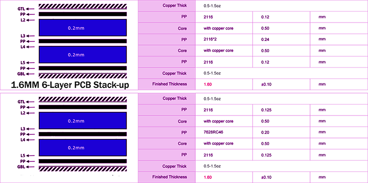
What are the Thickness of 6-Layer PCB standard Stackup?
The thickness of a 6-layer PCB (Printed Circuit Board) stackup can vary depending on the specific design requirements and manufacturing process.
1.6MM 6 Layer PCB Stack-up:
2.4MM 6 Layer PCB Stack-up:
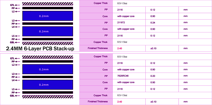
The standard thickness of a 6-layer PCB stackup can be around 1.6 to 2.4 millimeters (mm). However, keep in mind that these values are approximate and can vary based on the specific requirements of the PCB design and manufacturing process. It’s always best to consult with your PCB manufacturer or design guidelines to determine the exact stackup thickness for your project.
6 Layer PCB Stackup Applications
The utilization of 6-layer PCBs, as well as multi-layer PCBs, has gained significant prominence across diverse industries due to their exceptional wiring capabilities and superior performance.
Consumer Electronics: High-end consumer electronic products, including smartphones, wearable devices, and microwave ovens, frequently employ the 6-layer PCB stackup to accommodate their complex circuitry requirements.
Telecommunications: Telecommunication applications such as GPS devices, satellites, signal transmission systems, and base stations extensively rely on the utilization of 6-layer PCBs to ensure efficient and reliable communication.
Medical Devices: Medical equipment, such as scanning devices, X-ray machines, and heart monitors, extensively leverage 6-layer PCBs for their intricate circuitry needs, enabling accurate and precise medical diagnostics.
Industrial Control: 6-layer PCB stackups find significant applicability in industrial control systems. The durability and stability offered by these PCBs make them well-suited for industrial production environments, allowing seamless operation and adaptability to varying production conditions.
Advantages of 6-Layer Stack-ups
The incorporation of a 6-layer PCB stack-up provides numerous advantages in PCB design:
Enhanced Design Flexibility:
With additional layers, a 6-layer stack-up offers greater routing options and flexibility. This makes it well-suited for accommodating complex designs with higher component density, allowing for efficient placement and routing of components.
Improved Signal Integrity:
The inclusion of dedicated power and ground planes minimizes noise, crosstalk, and Electromagnetic Interference (EMI). This results in improved signal integrity and reliable data transmission, critical for ensuring the overall performance of the circuit.
Enhanced Power Distribution:
By utilizing dedicated power planes, a 6-layer stack-up ensures efficient power distribution throughout the PCB. This helps to reduce voltage drops, maintain a stable power supply, and minimize the potential for power-related issues.
Suitable for High-Density Designs:
6-layer stack-ups provide ample space for accommodating a larger number of components and intricate routing requirements. This makes them highly suitable for high-density designs where space optimization is crucial.
Cost-Effectiveness:
Despite offering increased functionality and design options, 6-layer stack-ups are generally more cost-effective compared to higher-layer configurations. This makes them a practical choice for balancing design requirements and production costs without compromising on performance.
Challenges Faced and Solutions Implemented of 6-Layer PCB Stackup
Challenges faced during the design and implementation of a 6-layer PCB stackup can vary depending on the specific requirements of the project. However, here are some common challenges and possible solutions that engineers may encounter:
Signal Integrity and Crosstalk:
Challenge: High-speed signals can be prone to signal integrity issues such as reflections, noise, and crosstalk due to the proximity of traces.
Solution: Careful consideration of trace spacing, controlled impedance routing, and proper placement of ground and power planes can help mitigate signal integrity issues. Signal integrity analysis tools can also be used to simulate and optimize signal performance.
Power Delivery and Grounding:
Challenge: Adequate power distribution and grounding are crucial for stable operation of the circuit. Inadequate power and ground planes can introduce voltage drops and noise.
Solution: Placing dedicated power and ground planes strategically in the stackup, using low impedance paths, and ensuring proper decoupling capacitor placement can help achieve proper power delivery and grounding.
Thermal Management:
Challenge: Components and high-power traces can generate heat, and inadequate thermal management can lead to performance degradation or component failures.
Solution: Proper placement of thermal vias, heat sinks, and thermal relief patterns in the PCB design can help dissipate heat effectively. Thermal analysis and simulation tools can aid in identifying potential hotspots and optimizing thermal performance.
Manufacturability and Layer Alignment:
Challenge: Achieving precise layer alignment during PCB fabrication can be challenging, leading to registration errors and impedance variations.
Solution: Collaboration with the PCB manufacturer during the design phase and following their guidelines for layer stackup can help ensure proper layer alignment and registration. Utilizing fabrication techniques such as laser drilling or sequential lamination can improve accuracy.
Design for Test (DFT):
Challenge: Accessing and testing the inner layers of the 6-layer PCB can be difficult without proper test points.
Solution: Including test points or vias in strategic locations to allow for testing and debugging of the inner layers. Collaborating with the test engineer to determine the necessary test points and implementing them in the design.
Cost and Size Constraints:
Challenge: Balancing the complexity of the PCB stackup design with cost and size constraints can be challenging, especially in compact and cost-sensitive designs.
Solution: Optimizing the layer count, considering the use of blind and buried vias, and selecting appropriate materials and manufacturing processes can help strike a balance between functionality, cost, and size constraints.
It’s important to note that these challenges and solutions are not exhaustive, and the specific challenges faced during a 6-layer PCB stackup design can vary depending on the project requirements and constraints. Working closely with experienced PCB designers and manufacturers, as well as utilizing simulation and analysis tools, can greatly help in addressing these challenges effectively.
What is the Best 6 Layer PCB Stackup?
Selecting the appropriate stack-up configuration for a PCB design is crucial, as it significantly impacts shielding, signal transmission, and the overall reliability of the final product. By considering the 6-layer PCB stack-up before fabrication, both time and cost can be saved.
One commonly used configuration by engineers is as follows:
●Top Signal layer
●Ground Plane layer
●Inner Signal layer
●Second Inner Signal layer
●Power Plane layer
●Bottom Signal layer
This stack-up configuration provides effective shielding for the signal layers, ensuring robust signal transmission and preventing potential faults. The inclusion of multiple layers adds an extra level of protection.
However, it’s important to note that this configuration results in a separation of the power and ground layers, leading to reduced capacitance. To address this, an alternative 6-layer PCB stack-up configuration can be considered:
●Single Top Signal layer
●Ground Plane layer
●Inner Signal layer
●Power Plane layer
●Single Ground Plane layer
●Bottom Signal layer
In this configuration, the ground and power layers are positioned close to each other, enabling improved capacitance for the circuit. This was previously regarded as one of the best practices for 6-layer PCB stack-up. It is essential to recognize that different applications may have distinct requirements, and the selection of the stack-up configuration should be carefully evaluated based on those specific needs.
Considerations Associated with 6-Layer PCB Stack-ups
Designing a 6-layer PCB stack-up requires careful consideration of several crucial factors. Some key considerations associated with 6-layer PCB stack-ups are:
Signal Integrity: Ensuring proper signal integrity is essential for reliable circuit performance. Careful layer arrangements, such as placing critical high-speed signals between adjacent ground or power planes, help minimize signal degradation, cross-talk, and noise.
Power Distribution: Effective power distribution is critical for supplying stable and clean power to components. Allocating dedicated power and ground planes strategically within the stack-up helps minimize power fluctuations, voltage drops, and EMI.
Layer Ordering and Placement: The order and placement of layers impact overall performance. Placing signal layers adjacent to ground or power planes provides better shielding and reduces EMI susceptibility. Strategically positioning layers based on component placement and signal flow helps optimize routing and minimize interference.
Controlled Impedance: Many high-speed signals require controlled impedance to prevent signal degradation. By incorporating specific layer thicknesses and dielectric materials, controlled impedance can be achieved. The stack-up configuration should consider controlled impedance requirements for critical signals.
EMI Shielding: Electromagnetic interference (EMI) can impact signal integrity. A well-designed stack-up includes shielding layers, such as ground planes and solid power planes, to provide effective EMI protection and prevent interference from internal and external sources.
Thermal Considerations: Thermal management is crucial to prevent overheating and maintain component reliability. Adequate copper plane area and heat dissipation considerations enable proper thermal distribution and help prevent thermal hotspots.
Manufacturing Feasibility: Stack-up options should also consider manufacturing feasibility. Alignment with PCB manufacturer capabilities, material availability, and impedance control during fabrication should be verified.
By carefully addressing these considerations during the planning and design phase, a well-optimized 6-layer PCB stack-up can be achieved, ensuring enhanced signal integrity, power distribution, EMI shielding, and overall reliable functionality of the circuit board.
The Importance of a 6-Layer Board Stackup in PCB Design
Multilayer printed circuit boards have become an integral aspect of modern design, adapting to advancements in electronic components and enabling increased circuitry integration. The evolution of electronic capabilities has necessitated the development of new PCB design and manufacturing technologies to cater to these requirements. While 6-layer board stackups were initially employed to accommodate additional traces compared to 2 or 4 layer boards, their significance has grown substantially.
Ensuring the correct configuration of layers in a 6-layer stackup has become paramount in maximizing circuit performance. Inadequate layer stackup configurations can render a PCB susceptible to electromagnetic interference (EMI) and result in poor signal performance. Conversely, a meticulously designed 6-layer stackup can address issues related to impedance and crosstalk, elevating the performance and reliability of the circuit board. Moreover, a well-planned layer stackup configuration can offer protection against external noise sources.
Conclusion
Designing a well-optimized 6-layer stack-up is of utmost importance when aiming to achieve the desired electrical performance, signal integrity, power distribution, and electromagnetic compatibility (EMC) in PCB designs. The utilization of a 6-layer stack-up offers various advantages, such as increased design flexibility, improved signal integrity, enhanced power distribution, and suitability for high-density designs. However, several crucial factors should be taken into account by designers.
Firstly, the complexity of the design, cost considerations, limitations in signal integrity, and feasibility of routing must be thoroughly evaluated when selecting a 6-layer stack-up configuration. Each of these factors can significantly impact the overall performance and manufacturability of the PCB design.
Achieving impedance control and maintaining signal integrity in 6-layer stack-ups requires meticulous planning, precise calculations, and strict adherence to established design guidelines. Proper consideration of trace widths, spacing, and layer thicknesses is essential to ensure accurate impedance matching and impedance control.
By carefully considering these factors, employing appropriate design techniques, and adhering to industry best practices, designers can ensure the reliable and efficient operation of their electronic circuits through the implementation of a well-designed 6-layer stack-up configuration.


