
We have prepared this definitive technical guide to assist your engineering and design teams in navigating the complexities of high-performance circuit board manufacturing with Taconic RF-60TC laminates. Our objective is to provide you with a comprehensive resource covering everything from fundamental material properties to our advanced fabrication processes and quality protocols.
This guide is intended for you—the innovators working in RF, microwave, 5G, aerospace, and medical electronics who cannot afford to compromise on performance. Here, you will find the detailed information necessary to confidently design, specify, and procure your Taconic RF-60TC PCBs, ensuring your most demanding projects are built for success.
What is Taconic RF-60TC?
Taconic RF-60TC is a specialized high-frequency laminate, engineered for applications where signal integrity and stability are governing factors. It is a ceramic-filled, woven glass reinforced Polytetrafluoroethylene (PTFE) composite. This composition gives it a distinct set of properties that make it a suitable choice for demanding electronic environments.
Material Composition and Structure
The material’s construction defines its performance. Each component has a specific function.
●PTFE Base: Provides exceptional electrical insulation and a very low dissipation factor, forming the basis for low-loss signal transmission. Its inherent hydrophobicity also ensures stable performance in humid conditions.
●Ceramic Filler: This additive enhances thermal conductivity and stabilizes the dielectric constant (Dk) across a wide range of temperatures and frequencies. The type and distribution of the ceramic filler are proprietary aspects that define the material’s performance characteristics.
●Woven Glass Reinforcement: Imparts mechanical strength and dimensional stability to the laminate, preventing warping and allowing for precise layer-to-layer registration during manufacturing. The style of the glass weave can also influence the dielectric properties and is a factor in precision designs.
Primary Use Cases
RF-60TC is not a general-purpose material; it is specified for circuits where certain performance metrics must be met.
●High-Frequency Circuits: Its primary application is in systems operating in the microwave and millimeter-wave (mmWave) spectrums, such as 5G infrastructure, satellite communications, and automotive radar.
●Power Amplifiers: The material’s thermal properties make it suitable for applications involving high-power components that generate significant heat, allowing for their operation within designated temperature limits.
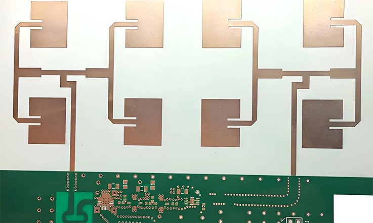
●Antenna Systems: Its stable dielectric constant enables the function of phased-array antennas and other radiating structures that require precise phase control and minimal signal degradation across the antenna feed network.
Core Electrical & Thermal Properties of Taconic RF-60TC
The performance of any high-frequency circuit is fundamentally linked to the properties of its substrate. Taconic RF-60TC is defined by a set of core electrical and thermal characteristics that allow designers to achieve a high degree of signal integrity, impedance control, and long-term operational reliability. Understanding these parameters is the first step in utilizing the material’s full potential.
Electrical Characteristics
These properties govern how electromagnetic waves travel through the material, directly affecting signal quality.
Key Electrical Parameters:
| Property | Value | Notes |
| Dielectric Constant (Dk) | 6.15 (X/Y Axis) | Enables accurate impedance control and compact circuit designs |
| Dissipation Factor (Df) | 0.0028 | Ensures minimal energy loss and high system efficiency |
| Volume Resistivity | 10⁸ MΩ·cm | Provides strong electrical isolation |
| Surface Resistivity | 10⁷ MΩ | Helps prevent crosstalk between adjacent traces |
Dielectric Constant (Dk): 6.15 (X/Y Axis)
●A stable Dk value allows for accurate impedance control (e.g., 50Ω). This value also enables more compact circuit designs compared to lower-Dk materials while maintaining precise transmission line performance.
●This stability results in the physical circuit performing as predicted by simulation models, reducing design iterations.
Dissipation Factor (Df): 0.0028
●This low value signifies minimal signal energy loss as the signal passes through the material. In many RF systems, every fraction of a decibel (dB) of loss can affect performance.
●This characteristic leads to maximized signal power, improved system efficiency, and an enhanced signal-to-noise ratio, benefiting sensitive receivers and high-power transmitters.
Volume & Surface Resistivity
●High resistivity values provide excellent electrical isolation between conductive elements on the PCB.
●This prevents current leakage and minimizes crosstalk between adjacent signal traces, even in dense circuit layouts, ensuring signals do not interfere with one another.
Thermal Characteristics
These properties determine how the material behaves under thermal stress, which has a direct bearing on device reliability and lifespan.
Key Thermal Parameters:
| Property | Value | Notes |
| Z-Axis CTE | 47 ppm/°C | Close to copper, reduces stress on vias and PTHs |
| Thermal Conductivity | 0.65 W/m·K | Promotes efficient heat dissipation from active components |
| Decomposition Temperature (Td) | >500°C | Supports high-temperature processes without degradation |
Z-Axis Coefficient of Thermal Expansion (CTE): 47 ppm/°C
●This low Z-axis CTE closely matches that of copper (which is ~17 ppm/°C). This compatibility is a primary factor for plated through-hole reliability.
●This match reduces mechanical stress on plated through-holes (PTHs) and vias during temperature cycling, preventing barrel cracking and supporting the long-term reliability of layer-to-layer connections in environments with fluctuating temperatures.
Thermal Conductivity: 0.65 W/m·K
●The ceramic filler enhances the material’s ability to conduct heat compared to standard PTFE laminates.
●This facilitates the dissipation of heat away from active components like amplifiers and processors, reducing peak operating temperatures, preventing performance throttling, and improving device longevity.
Decomposition Temperature (Td): >500°C
●The material can withstand high temperatures without degrading its chemical structure.
●This allows the PCB to maintain its structural integrity through multiple lead-free soldering and assembly processes, which often exceed 260°C.
A Comparative Analysis: Taconic RF-60TC Against Other Laminates
Selecting an RF laminate involves balancing performance, cost, and specific application requirements. Understanding how Taconic RF-60TC compares to other common options, such as those from Rogers Corporation or standard FR-4, provides our engineers with the context needed to make an informed choice.
Comparison with Rogers RO4350B
RO4350B is a hydrocarbon/ceramic laminate. The comparison highlights different design approaches and material capabilities.
Taconic RF-60TC vs Rogers RO4350B:
| Parameter | Taconic RF-60TC | Rogers RO4350B |
| Dielectric Constant (Dk) | ~6.15 (X/Y Axis) | ~3.48 |
| Dissipation Factor (Df) | 0.0028 @ 10 GHz | 0.0037 @ 10 GHz |
| Z-Axis CTE | ~47 ppm/°C | ~50 ppm/°C |
| Processing Requirements | PTFE-based (plasma) | Hydrocarbon-based |
| Manufacturing Complexity | Higher | Lower |
●Dielectric Constant (Dk): Taconic RF-60TC has a Dk of approximately 6.15, whereas Rogers RO4350B has a Dk of approximately 3.48. The higher Dk of RF-60TC allows for circuit miniaturization, as transmission line widths become smaller for a given impedance. The lower Dk of RO4350B is suitable for designs where physical size is a lesser constraint.
●Dissipation Factor (Df): At 10 GHz, RF-60TC exhibits a Df of about 0.0028, compared to about 0.0037 for RO4350B. The lower loss characteristic of RF-60TC makes it a superior option for very high-frequency (mmWave) or loss-sensitive applications, such as satellite links, where link budget margins are tight.
●Z-Axis CTE: Both materials exhibit a low Z-axis CTE (approx. 47 ppm/°C for RF-60TC, approx. 50 ppm/°C for RO4350B). This proximity to the CTE of copper means both materials offer excellent plated-through-hole reliability in designs that undergo significant temperature cycling.
●Manufacturing Process: RF-60TC is PTFE-based and requires specialized plasma processing for proper hole wall preparation. RO4350B is a hydrocarbon-based thermoset, which processes similarly to FR-4. As a result, RO4350B is generally less complex and less costly to manufacture. RF-60TC necessitates a manufacturing facility with specific expertise in PTFE processing to achieve high yields.
Comparison with Standard FR-4
FR-4 is the industry standard for most PCBs but is generally unsuitable for high-frequency RF applications. This comparison illustrates why specialized materials are specified.
Taconic RF-60TC vs Standard FR-4:
| Parameter | Taconic RF-60TC | Standard FR-4 | Notes |
| Dielectric Constant (Dk) | ~6.15 (Stable) | ~4.8 → ~4.2 (Variable) | FR-4 Dk varies with frequency; RF-60TC offers predictability |
| Dissipation Factor (Df) | 0.0028 | ~0.020 | FR-4 incurs high signal loss |
| Moisture Absorption | Very Low | High (Hygroscopic) | RF-60TC performance remains stable in humid environments |
| High-Frequency Suitability | Excellent | Poor | RF-60TC is optimized for GHz-range designs |
●Dielectric Constant (Dk): Taconic RF-60TC maintains a stable Dk of 6.15 across a wide frequency range. The Dk of standard FR-4 varies significantly with frequency, from approximately 4.8 down to 4.2 or lower. This instability in FR-4 makes predictable impedance control at RF frequencies unattainable.
●Dissipation Factor (Df): The Df of RF-60TC is approximately 0.0028. The Df of FR-4 is nearly an order of magnitude higher, at about 0.020. FR-4 absorbs and converts a large portion of RF signal energy into heat, resulting in severe attenuation over very short distances.
●Moisture Absorption: Taconic RF-60TC has a very low moisture absorption rate due to its PTFE base. FR-4 is hygroscopic, meaning it absorbs moisture from the air, which in turn alters its Dk and Df, causing performance to drift with environmental humidity. The stability of RF-60TC makes it suitable for deployment in any environment.
Design & Layout Principles for RF-60TC PCBs
Designing with Taconic RF-60TC requires adherence to a set of principles that differ from standard digital PCB design. The goal is to manage electromagnetic fields, control impedance, and minimize signal loss. A successful design leverages the material’s properties through disciplined layout and structuring.
Controlled Impedance Transmission Lines
At high frequencies, PCB traces act as transmission lines. Their geometry must be precisely controlled.
●Microstrip: A trace on an outer layer with a solid ground plane below it. This is a common configuration but is more susceptible to radiation and external interference.
●Stripline: A trace on an inner layer, sandwiched between two ground planes. This offers superior shielding and isolation, containing the EM fields and preventing crosstalk. It is a preferred choice for sensitive or high-density routing.
●Coplanar Waveguide (CPW): A trace with ground planes on both sides on the same layer, often connected with via stitching. This is useful for isolating RF signals without requiring adjacent layers and for facilitating on-wafer probing.
●Trace Calculation: Engineering support can assist clients in calculating the precise trace widths and spacing needed to achieve target impedances (e.g., 50Ω) for each of these configurations based on the RF-60TC stack-up, taking into account factors like the final copper thickness and solder mask effects.
Grounding and Return Path Management
A clean, low-inductance ground system is foundational to a high-performance RF design. The return current will always seek the path of least impedance, which at high frequencies is the path of least inductance, not least resistance.
●Solid Ground Planes: Always use continuous, solid ground planes as the reference for high-frequency signals. Routing traces across splits or voids in the ground plane forces the return current to take a long, circuitous path, creating a large current loop that radiates noise and degrades signal integrity.
●Via Stitching: Placing rows of ground vias along the edges of RF traces and around the board perimeter forms a “via fence.” This structure helps contain electromagnetic fields and provides a short, direct path for return currents, improving isolation and suppressing unwanted cavity resonance modes within the PCB.
Layer Stack-up and Configuration
The arrangement of layers in a PCB is an architectural decision that affects performance, cost, and manufacturability.
●4-Layer Stack-up: A common recommendation for many RF designs. A structure of Signal-Ground-Power-Signal provides good shielding for the signal layers from power distribution noise.
●Multilayer Stack-ups: For complex mixed-signal designs, multiple ground and power layers are used to isolate noisy digital sections from sensitive analog/RF sections. Careful planning of layer assignments is a core step.
●Symmetry: Designing a symmetrical stack-up (where the layer types and thicknesses are mirrored around the center) helps balance mechanical stresses during the high-temperature lamination process, preventing board warpage. This has a direct bearing on large or thin PCBs.
The Impact of Copper Surface Roughness on Signal Loss
At frequencies deep into the GHz range, especially in the mmWave spectrum, second-order effects become dominant sources of signal loss. One of the most pronounced of these is the surface roughness of the copper foil used in the PCB laminate. Managing this variable is a component of high-precision circuit board manufacturing.
Skin Effect and Surface Roughness
The interaction between these two phenomena is central to understanding high-frequency losses.
●Skin Effect: At high frequencies, electrical current concentrates in a very thin layer near the conductor’s surface, known as the “skin depth.” As frequency increases, the skin depth decreases. At 28 GHz, the skin depth in copper is less than 0.4 µm.
●Surface Roughness: Copper foil surfaces are not perfectly smooth; they have microscopic peaks and valleys. When the skin depth becomes comparable to the height of this surface roughness, the effective path length for the current increases. The current is forced to travel up and down the microscopic topography, increasing the total resistive loss.
●The Cannon-Morgan Model: This is an industry-standard model used to quantify the additional signal loss due to copper roughness. It calculates a “roughness correction factor” that is applied to standard conductor loss calculations for more accurate modeling.
Types of Copper Foil and Their Impact
The type of copper foil laminated to the Taconic RF-60TC substrate has a direct effect on performance.
●Standard Electrodeposited (ED) Copper: This is a common type of foil. It has a relatively high surface roughness profile, which promotes good mechanical adhesion but can lead to increased signal loss at mmWave frequencies.
●Reverse-Treated (RT) Foil: This foil has one smooth side and one rough side. The laminate is constructed so that the smoother side is used for etching the circuit traces, providing a better surface for high-frequency signals, while the rougher side ensures strong adhesion to the dielectric.
●Rolled-Annealed (RA) Copper: This is a high-performance option. RA foil is produced by mechanically rolling copper ingots, resulting in a very smooth, dense surface profile. It offers the lowest possible signal loss but can have lower peel strength and is a higher-cost option.
Manufacturing and Material Control
Boards can be built with the appropriate copper foil for a given application.
●Material Specification: Taconic RF-60TC laminates can be procured with different types of copper foils based on specific loss budget and performance requirements.
●Process Control: Etching processes are carefully controlled to avoid excessively roughening the copper surface, preserving the inherent low-loss characteristics of the chosen foil.
●Simulation Support: Guidance is available on how to correctly model the effects of copper roughness in EM simulation software to ensure loss predictions are accurate.
Mitigating Passive Intermodulation (PIM) in PCB Design
Passive Intermodulation (PIM) is a form of signal interference of major concern in high-power, multi-carrier communication systems, such as 5G base stations and satellite links. It occurs when two or more strong signals mix in a non-linear passive device, creating unwanted new frequencies that can fall into the system’s receive band, desensitizing the receiver and degrading performance. The PCB itself can be a source of PIM.
PIM Causes in a PCB
PIM arises from non-linearities in the RF path. In a PCB, these non-linearities can be caused by several factors.
●Material Interfaces: The junction between the copper trace and the surface finish can create a slight non-linearity, especially with certain metallic layers like nickel (used in ENIG), which is ferromagnetic.
●Connector Junctions: The area where an RF connector attaches to the PCB often becomes a key contributor to passive intermodulation. Factors such as substandard soldering, leftover flux, or variable contact force can introduce unwanted non-linear behaviors.
●Ferromagnetic Materials: Any trace of ferromagnetic materials (iron, nickel, cobalt) in the signal path can generate high levels of PIM when subjected to strong magnetic fields from the RF signals.
●Current Density Variations: Sharp corners, nicks, or scratches on a trace can cause current to bunch up, leading to localized non-linear heating and PIM generation.
PCB Design and Manufacturing Techniques to Minimize PIM
Specific techniques and controls can be employed to produce low-PIM PCBs.
●Low-PIM Surface Finishes: For applications with stringent PIM requirements, Immersion Silver or specialized low-PIM tin finishes are often preferred as they avoid the ferromagnetic nickel layer present in ENIG.
●Cleanliness and Process Control: The manufacturing sequence emphasizes extreme cleanliness. It ensures that no residues from etching, plating, or handling contaminate the final board, as these can be sources of PIM.
●Trace and Edge Quality: Precision etching creates smooth, uniform trace edges, free from nicks and scratches. Board routing is also done carefully to ensure clean edges without loose copper slivers.
●Connector Pad Design: Land patterns for RF connectors can be optimized to promote a robust and consistent solder joint, which contributes to a low-PIM transition from the board to the cable.
A System-Level Approach
Minimizing PIM requires a system-level perspective.
●Collaboration: Coordination between the design function, connector suppliers, and assembly groups helps ensure every part of the signal path is optimized for low-PIM performance.
●Material Selection: The choice of Taconic RF-60TC itself, with its stable and uniform dielectric properties, provides a solid, linear foundation for building low-PIM circuits.
Navigating Signal Integrity Challenges at Millimeter-Wave Frequencies
Designing for millimeter-wave (mmWave) frequencies—generally from 24 GHz to 300 GHz—introduces a new set of signal integrity challenges. At these wavelengths, the physical features of the PCB become a significant fraction of a wavelength, and every element of the design must be treated as a complex electrical component. Taconic RF-60TC is a suitable substrate for this domain, but successful application requires a deep understanding of these mmWave effects.
Dominant Loss Mechanisms
At mmWave frequencies, the total insertion loss of a transmission line is a primary performance metric, dominated by several factors.
●Dielectric Loss: The energy dissipated as heat within the substrate. This is directly proportional to the frequency and the material’s dissipation factor (Df). RF-60TC’s low Df plays a main role in reducing this thermal loss.
●Conductor Loss: The resistive loss in the copper trace. As explained previously, this is exacerbated by the skin effect and copper surface roughness.At millimeter-wave frequencies, this type of loss typically represents the most significant portion of the overall signal attenuation.
●Radiation Loss: Energy that radiates away from the transmission line into the surrounding space or adjacent layers. This can be controlled with design practices such as using stripline configurations or tightly coupled coplanar waveguides.
Phase and Dispersion Effects
Maintaining the phase relationship between signals is fundamental for applications like beamforming in phased-array antennas.
●Phase Velocity: The speed at which a signal’s phase travels along a transmission line, determined by the dielectric constant. The stability of RF-60TC’s Dk results in a stable and predictable phase velocity.
●Dispersion: This is the phenomenon where different frequency components of a signal travel at slightly different speeds, which can distort wideband signals. The woven glass reinforcement in a PCB laminate can introduce dispersion, an effect that can be modeled and mitigated through careful trace orientation and routing.
Parasitic Effects and Discontinuities
At mmWave frequencies, every small physical feature can have a large electrical impact.
●Via Transitions: A via is not a simple short circuit; it is a 3D structure with parasitic capacitance and inductance that can cause reflections and signal loss. Optimizing via pad and antipad sizes, and using techniques like back-drilling to remove unused via stubs, are methods to improve performance.
●Surface Wave Propagation: Under certain conditions, EM energy can get trapped and propagate along the surface of the dielectric, coupling into and interfering with other parts of the circuit. Layout techniques, such as using via fences, can suppress these unwanted surface wave modes.
Advanced Thermal Management Techniques for High-Power RF Applications
While Taconic RF-60TC has better thermal conductivity than standard PTFE, high-power RF applications like solid-state power amplifiers (SSPAs) often require more aggressive thermal management strategies. Efficiently removing heat from active devices affects performance, stability, and long-term reliability. Advanced thermal solutions can be implemented directly into the PCB structure.
Thermal Vias
This is a common and effective method for transferring heat vertically through the PCB.
●Mechanism: An array of plated through-holes is placed directly under a heat-generating component. These vias act as parallel heat conductors, transferring thermal energy from the component on the top layer down to a ground plane or a heatsink attached to the bottom layer.
●Design Considerations: The effectiveness of thermal vias depends on their diameter, plating thickness, and density. A dense array of open vias is often more effective at heat transfer than fewer, larger vias. They can also be filled with conductive or non-conductive epoxy.
Heatsink Integration and Copper Coins
For extreme heat loads where thermal vias are insufficient, more advanced solutions can create a direct, low-resistance thermal path.
1.Pedestal and Embedded Coins: A solid piece of copper (a “coin”) can be embedded into a cutout in the PCB. The active component is then mounted directly onto this coin. This creates a direct, uninterrupted thermal path from the component to an external heatsink.
●Press-fit Coins: The coin is physically pressed into a milled cavity after the main PCB lamination.
●Embedded Coins (Coin-Inlay): The coin is integrated during the lamination process itself for a more seamless structure, offering the lowest possible thermal resistance.
2.Heatsink Attachment: The PCB design can include appropriate mounting holes, thermal interface material (TIM) considerations, and surface finishes (e.g., bare copper or ENIG) to allow for a low-resistance connection to an external chassis or heatsink.
Heavy Copper and Thermal Spreading
Using thicker copper layers can enhance a board’s ability to spread heat laterally, reducing the temperature gradient across the board.
●Copper Weight: Standard PCBs use 1 oz (35 µm) copper. For high-power applications, boards can be constructed with “heavy copper”—2 oz, 3 oz, or more—on ground and power planes.
●Heat Spreading: These thick copper layers act as effective heat spreaders, drawing thermal energy away from localized hot spots under components and distributing it over a wider area of the board, which lowers the peak temperature.
Specialized Manufacturing for Taconic RF-60TC PCBs
The manufacturing of circuits with Taconic RF-60TC is different from processing standard FR-4. Its PTFE and ceramic composition requires specialized equipment and controlled processes. A facility for these advanced materials ensures that the finished PCB matches design intent and performance specifications.
Drilling and Hole Wall Preparation
The reliability of a multilayer RF board is determined by the quality of its vias.
●Precision Drilling: Specialized drill bits and controlled entry/exit materials are used to produce clean holes with minimal burring. Drill speeds and feed rates are optimized to prevent heat buildup and the smearing of PTFE material on the hole wall.
●Plasma Desmear: This is a standard step for all PTFE-based materials. After drilling, boards are placed in a plasma chamber where a gas mixture (including oxygen and CF4) etches the hole wall. This action removes any drill smear and chemically activates the surface, creating a microroughened texture for strong copper plating adhesion.
Lamination and Etching Control
These processes define the physical structure and circuitry of the board.
●Controlled Lamination: Lamination presses use precise temperature and pressure profiles designed for RF-60TC and its bonding materials. This ensures complete bonding between layers without altering the material’s sensitive electrical properties or inducing excessive stress.
●Etching Precision: Advanced etching processes achieve tight control over trace width and spacing. This precision allows for the creation of accurate geometries for controlled impedance transmission lines. Etch factors are compensated for to ensure the final trace dimensions are as specified.
Surface Finish Application
The surface finish is the interface for component soldering and high-frequency signal flow. The choice is driven by frequency, cost, and assembly method.
●Electroless Nickel Immersion Gold (ENIG): An industry standard for many RF applications. It provides a flat, solderable, and corrosion-resistant surface, suitable for fine-pitch components like BGAs and QFNs.
●Immersion Silver (ImAg): Offers excellent performance at high frequencies due to its low resistivity and very smooth surface. It is a preferred choice for mmWave and low-PIM applications but requires handling in a manner that prevents tarnishing.
●Other Finishes: Other available finishes include ENEPIG (which adds a palladium layer for improved wire bonding reliability) and Immersion Tin, based on specific application requirements for wire bonding or press-fit connectors.
Mastering Hybrid Builds: Integrating RF-60TC with FR-4
A pure Taconic RF-60TC construction offers maximum performance, but for many complex designs, a hybrid or mixed-dielectric approach provides an effective balance of performance and cost. This involves combining layers of RF-60TC with standard FR-4 in a single PCB stack-up. Executing this reliably requires addressing significant material compatibility challenges.
The Rationale for Hybrid Stack-ups
This approach is driven by both cost and function.
●Cost Optimization: Use premium RF-60TC layers only for high-frequency signal paths. Use inexpensive FR-4 for non-critical layers, such as low-speed digital control and power distribution. This can reduce overall board cost without compromising RF performance.
●Mechanical Rigidity: FR-4 is more rigid than PTFE-based laminates. Incorporating FR-4 layers can add stiffness and robustness to the final PCB assembly.
The CTE Mismatch Challenge
The primary technical hurdle is the difference in the Coefficient of Thermal Expansion (CTE) between the two materials.
●The Problem: During thermal cycling, FR-4 expands and contracts at a different rate than RF-60TC. This creates mechanical stress that can lead to board warpage, delamination, or place strain on vias that pass through both material types.
●The Solution: This can be mitigated through several techniques:
1.Optimized Lamination Cycles: Using a slow temperature ramp and a low-pressure press cycle allows the materials to bond without locking in excessive stress.
2.Specialized Bonding Materials: Selecting prepregs and bondplies that are designed to adhere to both PTFE and FR-4 surfaces helps buffer the mechanical stress.
3.Symmetrical Design: Designing a stack-up that is symmetrical around the board’s center line helps balance the mechanical forces and produce a flat, stable board.
DFM for Hybrid Reliability
Design choices affect the success of a hybrid build.
●Layer Transition Vias: Vias that transition between the RF and FR-4 sections of the board require attention during the drilling and plating process to ensure a reliable connection across the material interface.
●Copper Balancing: Uniform copper distribution across all layers helps to minimize warpage by creating a more mechanically balanced structure.
The Role of DFM in High-Frequency PCB Success
Design for Manufacturability (DFM) is a collaborative philosophy that bridges the gap between circuit design and physical assembly. For high-frequency PCBs made with sensitive materials like Taconic RF-60TC, a proactive DFM review can identify and correct potential issues before they lead to fabrication delays, low yields, or performance failures.
DFM Checks Specific to RF Designs
Beyond standard DFM, RF designs undergo a specialized set of checks.
●Acid Traps and Copper Slivers: Checks for acute angles in traces that can trap etching chemicals, or thin slivers of copper that could detach and cause shorts.
●Via-in-Pad Protection: When vias are placed directly in component pads, they can be filled and plated over to prevent solder wicking, which can lead to poor solder joints.
●Solder Mask Dam Integrity: Verification of an adequate solder mask “dam” between fine-pitch component pads prevents solder bridging during assembly.
●Reference Plane Integrity: The DFM process includes a check to ensure that high-speed traces do not cross splits or voids in their reference ground planes.
Panelization and Depanelization Strategy
How individual boards are arranged on a panel can affect yield and quality.
●Routing vs. V-Scoring: For RF-60TC, precision routing with specialized bits is preferred over V-scoring. Routing creates a clean, smooth board edge and prevents the mechanical stress and PTFE fiber fraying associated with V-scoring.
●Fiducials and Tooling Holes: Panel designs include appropriately placed global and local fiducial marks for automated inspection and component placement, as well as tooling holes for secure fixture in manufacturing and testing equipment.
The Collaborative DFM Process
The process is designed to be interactive and transparent.
●DFM Report: After an analysis of the Gerber files, an illustrated report is provided, detailing any identified risks or suggested improvements.
●Engineering Consultation: RF engineers can be made available to discuss the DFM findings with a design team, explain the rationale behind suggestions, and work together to find a suitable solution that preserves design intent while maximizing manufacturability.
Signal Integrity & Validation with Advanced Testing
For high-frequency PCBs, functional verification requires more than a simple continuity test. It uses sophisticated measurement techniques to validate that the board’s electrical performance meets its design specifications. A quality assurance program can include a suite of testing protocols to guarantee the signal integrity and impedance control of Taconic RF-60TC boards.
Impedance Control Verification
Quantitative proof can be provided that controlled impedance traces meet their target values.
●Test Coupons: Specialized test coupons are fabricated on the same panel as the main boards. These coupons contain trace structures identical to those in the design.
●Time Domain Reflectometry (TDR): A TDR is used to send a calibrated pulse through the test coupon traces. By analyzing the reflections, the characteristic impedance along the length of the trace can be measured with high precision.
●Certified Report: Shipments requiring impedance control can be accompanied by a TDR report detailing the specified impedance, the measured values, and pass/fail status, providing traceability and verification.
RF Performance Characterization
For demanding applications, the RF performance of the finished board can be characterized.
●Vector Network Analyzer (VNA) Testing: Using a VNA and high-frequency probes, the S-parameters (Scattering parameters) of circuits can be measured directly on the PCB or on test coupons.
●Performance Metrics: This allows quantification of performance metrics:
1.Insertion Loss (S21): Measures the signal power lost as it travels through a trace.
2.Return Loss (S11): Measures the signal reflected back to the source due to impedance mismatches.
3.Crosstalk: Measures the unwanted signal coupling between adjacent traces.
Final Inspection and Reliability Standards
Every board undergoes a final inspection before shipment.
●Automated Optical Inspection (AOI): Used on inner and outer layers to verify trace integrity, spacing, and absence of defects against the original Gerber data.
●IPC-A-600 Standard: Inspectors are trained and certified to IPC-A-600, the standard for PCB acceptability. Boards can be inspected to Class 2 or the more stringent Class 3 requirements for aerospace, medical, and defense applications upon request.
Proven Success: Featured Case Study Summaries
The ultimate measure of a material and its fabrication is performance in the field. Below, we present summaries of representative case studies that highlight how precision-built Taconic RF-60TC PCBs solve challenges in demanding sectors. Each summary is a testament to a collaborative engineering process that results in measurable success.
Case Study: 5G mmWave Massive MIMO Antenna
●Challenge: A client required a large-format beamforming network for a 64T64R antenna. The primary obstacles were maintaining precise phase consistency across the entire array and minimizing insertion loss to maximize radiated power and cell coverage.
●Solution: A 12-layer hybrid stack-up was engineered, using Taconic RF-60TC for the RF feed network. Precision etching and lamination processes ensured that the material’s stable Dk translated into predictable phase performance, while the low loss of RF-60TC preserved signal power.
●Outcome: The final assemblies demonstrated phase variation under ±2°, exceeding the client’s specification. The measured insertion loss was 0.5 dB lower than with their previous substrate, directly contributing to a measurable increase in network throughput and operational range.
Case Study: Satellite Communications (SATCOM) Transceiver
●Challenge: An aerospace client needed a high-reliability transceiver module for a Ku-band satellite. The design faced extreme thermal cycling in orbit, making the long-term integrity of plated through-holes a primary concern. Effective heat dissipation from a high-power amplifier (HPA) was also mandated.
●Solution: A 10-layer pure RF-60TC board was constructed. The material’s low Z-axis CTE was leveraged to ensure via robustness. A dense array of thermal vias was designed directly beneath the HPA, creating an efficient thermal conduit to a chassis-mounted heatsink.
●Outcome: The modules successfully passed the client’s rigorous thermal vacuum chamber testing, which included 1,000 temperature cycles. Post-test analysis showed no degradation in via integrity or RF performance, confirming the design’s long-term reliability for space applications.
Case Study: Medical Imaging RF Coil
●Challenge: A medical device company was developing a new generation of Magnetic Resonance Imaging (MRI) surface coils. The design required extremely high signal-to-noise ratio (SNR) to produce clear, high-resolution images. The RF circuits had to be perfectly balanced and exhibit very low signal loss.
●Solution: A complex, large-format 8-layer board was fabricated from Taconic RF-60TC. The material’s very low dissipation factor was a key enabler. Controlled impedance routing and balanced trace-pair geometries were executed with exceptional precision to maintain signal purity and prevent phase imbalances.
●Outcome: The resulting RF coils achieved a 15% enhancement in signal-to-noise ratio over the earlier design, enabling clinicians to obtain clearer diagnostic images in less time. The controlled production process guaranteed reliable performance across every coil in the batch.
Full-length engineering case studies containing detailed performance data for these and other projects are available upon request to qualified partners.
Synthesis of Advantages: Your Pathway to System Success
Having explored the deep technical attributes of Taconic RF-60TC and the precision manufacturing processes required, it becomes clear how these elements translate into tangible success for your final product. The choice of substrate and its manufacturing is not merely a component decision; it is an investment in the performance and reliability of your entire system.
Achieve Uncompromising Signal Integrity:
By leveraging the material’s low dissipation factor, stable dielectric constant, and our control over factors like copper roughness and PIM, your design can achieve maximum signal power, clarity, and data throughput. This translates directly to better performance in your communication links, clearer images from your radar systems, and more sensitive receivers.
Ensure Long-Term Reliability:
The combination of low Z-axis CTE, excellent thermal management, and robust via formation techniques means your device is built to withstand demanding operational environments. This ensures your products operate flawlessly in the field for their entire intended lifespan, protecting your reputation and reducing total cost of ownership.
Enable Advanced and Compact Designs:
The high dielectric constant allows for device miniaturization without sacrificing performance. Our precision fabrication capabilities enable you to implement complex, dense layouts, giving your design team the freedom to innovate and create next-generation products within smaller form factors.
Build on a Foundation of Predictable Performance:
Our collaborative DFM process and advanced testing protocols remove uncertainty from the manufacturing process. When you receive your boards, you can be confident that they are a precise physical realization of your simulated models, allowing your project to move smoothly from assembly to deployment.
Technical Resources & Engineering Support
We believe in a partnership model that extends beyond fabrication. Our goal is to empower your design team with the resources and expertise needed to optimize your Taconic RF-60TC project from the very beginning. Our support can significantly accelerate your development cycle and improve the outcome of your design.
Our Design and Stack-up Guides
We offer these practical guides with clear recommendations to streamline your design process and help ensure your layout is optimized for high-frequency performance and manufacturability.
Design Resource Overview:
| Resource Type | Description | Purpose |
| Example Stack-up Library | Pre-approved layouts for 2-layer, 4-layer, and multilayer builds | Provides optimized starting points for RF-60TC design |
| Impedance Calculation Tables | Trace width & spacing data for 50Ω and 75Ω configurations | Supports accurate impedance control on microstrip and stripline traces |
| Thermal Management Design Patterns | Reference layouts for via arrays and copper pouring techniques | Helps designers implement effective thermal strategies |
●Example Stack-up Library: We invite you to access our collection of pre-approved stack-ups for 2-layer, 4-layer, multilayer, and hybrid builds. Each example is tailored for specific applications, providing a proven starting point for your design.
●Impedance Calculation Tables: We provide detailed tables with pre-calculated trace width and spacing dimensions for achieving 50Ω and 75Ω impedance on microstrip and stripline structures using RF-60TC.
●Thermal Management Design Patterns: You can explore our reference layouts demonstrating best practices for thermal design, including patterns for thermal via arrays and guidelines for copper pouring.
Our In-Depth Technical Papers and Application Notes
We encourage you to dive deeper into complex topics with our library of technical documentation, written by our senior RF engineers.
●Paper: “Mastering Hybrid Lamination with PTFE and FR-4”: A detailed review of challenges and solutions for managing CTE mismatch.
●Paper: “Signal Integrity at mmWave Frequencies”: A guide to layout techniques for minimizing insertion loss and crosstalk above 24 GHz.
●Note: “Choosing the Right Surface Finish for Your RF Application”: A comparative analysis of ENIG, ENEPIG, ImAg, and other finishes.
Request Your Custom Taconic RF-60TC PCB Quote
Embark on your next high-performance RF project with confidence. Partnering with us gives you access to unparalleled fabrication expertise for Taconic RF-60TC PCBs circuit board, ensuring your designs for 5G, aerospace, and medical applications are realized with precision and reliability. Our streamlined quoting process and dedicated engineering support ensure your custom-built PCBs arrive on time and to your exact specifications.
Let Us Provide Your Custom, Transparent Quote
We will provide clear, comprehensive pricing and lead time information tailored specifically to your Taconic RF-60TC design.
●Fast and Easy Submission: Securely upload your Gerber files, stack-up details, and fabrication notes through our online portal. Our engineering team will promptly review your data to provide a detailed quotation.
●Flexible Volume Options: We cater to all your needs, from rapid-turnaround prototypes for your initial validation to mid- and high-volume production runs.
●No Hidden Costs: Your quote will provide a complete and transparent breakdown of all costs, including raw materials, specific process requirements, your chosen surface finish, and all testing protocols.
Leverage Our Pre-Quote DFM Engineering Support
We encourage you to collaborate with our RF PCB engineers to streamline your build for optimal signal integrity and thermal management.
●Stack-up and Layout Guidance: We can provide recommendations on your layer planning and routing strategies to achieve the best performance with Taconic RF-60TC laminates.
●Controlled Impedance Planning: Let us assist you with specific trace width and spacing calculations to maintain consistent impedance across all your high-frequency signal paths.
●DFM Review: Our thorough analysis of your design files ensures they are optimized for our manufacturing processes, preventing potential fabrication issues.
Depend on Our Global Shipping and Secure Packaging
We understand that your custom PCBs are a high-value investment. We take every precaution to ensure they are protected during transit and arrive ready for your immediate assembly.
●Secure, Protective Packaging: All RF PCBs are handled with care, using anti-static materials, vacuum sealing, and moisture barrier bags to maintain board quality during transit.
●Flexible Logistics Solutions: We offer a range of global shipping options to meet your specific schedules, from express door-to-door couriers to freight solutions.
●Complete Shipment Visibility: From the moment your order leaves our facility, you will receive full tracking information, allowing you to monitor its progress and plan for its arrival.
FAQs for Taconic RF-60TC PCBs
Q: How are the board edges finished during routing or depanelization?
A: Precision routing with specialized bits is employed to prevent smearing of the PTFE and to ensure clean, well-defined board edges.
Q: Are there specific lamination parameters for multilayer builds?
A: Yes, a tightly controlled temperature and pressure cycle, specific to RF-60TC, is used to ensure proper layer bonding and dimensional stability without damaging the material.
Q: Is laser drilling applicable for creating microvias on RF-60TC?
A: Yes, laser ablation can form microvias. A UV laser with specific power and pulse settings is used to cleanly remove the substrate material without excessive heat damage.
Q: What is the primary challenge when laminating RF-60TC with FR-4 in a hybrid build?
A: The main challenge is managing the different coefficients of thermal expansion (CTE) between the materials. The lamination cycle is carefully optimized to minimize internal stress and ensure long-term reliability.
Q: How does plasma treatment for RF-60TC differ from standard PTFE materials?
A: Due to its high ceramic filler content, the gas mixture and treatment time for RF-60TC are adjusted to ensure uniform surface activation across the hole wall, which differs from pure or glass-reinforced PTFE.


