
Taconic RF-60A is a specialized PTFE-based PCB material designed to meet the needs of high-frequency applications, including RF and microwave systems. Known for its exceptional electrical performance and stability, RF-60A offers low signal loss and consistent performance across a range of demanding environments. This material excels in applications such as 5G base stations, satellite communication, automotive radar, and IoT devices. Through its precise dimensional control, superior laminate properties, and compatibility with various surface finishes and stack-ups, RF-60A ensures optimal performance in even the most challenging conditions. In the following sections, we’ll break down the key features, manufacturing techniques, and design considerations that make Taconic RF-60A an excellent choice for high-frequency circuit designs.
Understanding Taconic RF-60A PCB Materials and Laminate Properties
Designing RF and microwave PCBs isn’t just about copper thickness or trace width—it starts at the core: the laminate. Taconic RF-60A PCB materials are engineered for RF circuit structures that operate in the GHz range, offering dependable electrical behavior, stable performance under heat, and low loss. These materials are favored in applications like aerospace radar systems, 5G communication hardware, and RF power amplifiers, where signal degradation just isn’t an option.
RF-60A’s PTFE-ceramic blend sets it apart in applications that demand tight impedance control, low insertion loss, and high reliability in humid or high-temp conditions. The material offers not only measurable stability but also production consistency, which helps us maintain quality across multiple production runs.
PTFE-Based Taconic RF-60A Laminates: Composition and Characteristics
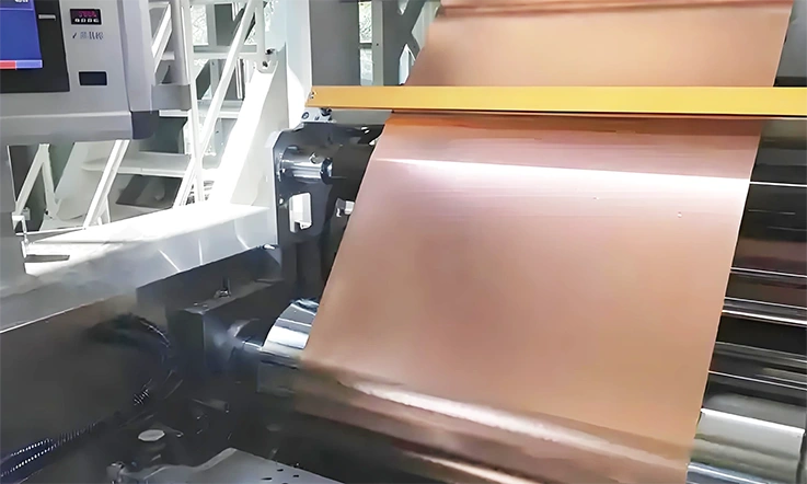
Taconic RF-60A PCB laminates are made with ceramic-filled polytetrafluoroethylene (PTFE) and reinforced fiberglass cloth. This structure ensures solid electrical integrity and dimensional predictability, even when subjected to reflow temperatures or multilayer lamination.
What this means for your project:
●Dielectric Constant (Dk): Nominally 6.15 ± 0.25 at 10 GHz—useful for impedance-sensitive RF trace design.
●Dissipation Factor (Df): As low as 0.0028 at 10 GHz—ideal for minimizing signal loss across frequency lines.
●Thermal Conductivity: 0.54 W/m·K—helps dissipate localized heating in power-carrying layers.
●Moisture Absorption: 0.02%—reduces the risk of dielectric shifts or delamination in harsh environments.
●CTE Z-axis: 69 ppm/°C—useful for maintaining plated-through-hole stability during thermal cycling.
Core Property Table – RF-60A Laminate-
| Property | Typical Value | Testing Standard |
| Dielectric Constant (10 GHz) | 6.15 ± 0.25 | IPC-TM-650 2.5.5.6 |
| Dissipation Factor (10 GHz) | 0.0028 | IPC-TM-650 2.5.5.5 |
| Moisture Absorption | 0.02% | IPC-TM-650 2.6.2.1 |
| Thermal Conductivity | 0.54 W/m·K | ASTM F433 |
| Z-axis CTE | ~69 ppm/°C | ASTM D3386 |
Dielectric Constant (Dk) and Dissipation Factor (Df) Performance
For microwave engineers and PCB designers, dielectric performance drives nearly every decision in the signal layer stackup. Taconic RF-60A PCB materials offer tight control over dielectric properties across both sheet and batch production. This means you can route RF lines and microstrip structures without running into inconsistent impedance or phase delay shifts.
Performance benefits:
●The Dk sits reliably at ~6.15, with low variation, keeping simulation results close to measured behavior.
●A Df of 0.0028 reduces attenuation over long traces, making this a go-to material for phased array radar, high-frequency antennas, or GPS receivers.
Moisture Absorption, Thermal Stability, and Dimensional Control
PTFE-based laminates are known for moisture resistance, but Taconic RF-60A PCB laminates take it a step further with optimized filler ratios and tight process control. This helps reduce dielectric drift in humid environments and allows reliable adhesion during reflow or lamination.
Here’s what that looks like on the shop floor:
●Moisture resistance: Keeps water uptake at just 0.02%, making it a solid choice for naval, aerospace, and outdoor RF systems.
●Thermal endurance: Maintains structure through multiple thermal cycles, even when exposed to solder reflow temperatures near 260°C.
●Dimensional predictability: Thanks to reinforced glass cloth and uniform filler dispersion, layer registration holds tight across panel sizes—even on large multilayer builds.
Mechanical Performance Summary-
| Mechanical Property | MD / CD Values | Testing Method |
| Tensile Strength | 19,500 / 16,300 psi | ASTM D3039 |
| Flexural Strength | 18,300 / 14,600 psi | ASTM D790 |
| Copper Peel Strength (1 oz) | ≥ 6 lbs/in | IPC-TM-650 2.4.8 |
Pro tip: When dealing with high-layer count boards, RF-60A’s low in-plane expansion helps prevent misregistration and drill breakout.
Taconic RF-60A PCB Design Guidelines for High-Frequency Applications
Designing high-frequency PCBs requires a detailed approach to materials, stack-up, and layout to ensure optimal performance. Taconic RF-60A, known for its low loss and consistent dielectric properties, offers a stable foundation for RF and microwave circuits. This section addresses best practices for controlling impedance, planning stack-ups, and laying out circuits to minimize signal reflection and optimize transmission.
Controlled Impedance and Signal Integrity Considerations
In high-frequency layouts, maintaining controlled impedance supports consistent signal transmission. Taconic RF-60A provides a stable dielectric constant (Dk) of 6.15 ±0.25 at 10 GHz, which minimizes signal loss and ensures predictable behavior in high-frequency applications.
To achieve controlled impedance, we need to calculate trace widths based on the target impedance (typically 50Ω for single-ended traces and 100Ω for differential pairs) and the Dk of the material. Taconic RF-60A’s stable Dk reduces the chances of impedance mismatches, preventing signal degradation or reflections.
The use of vias should be minimized since they can cause impedance discontinuities. Carefully placed vias help maintain stable return paths, but overuse can introduce unwanted resistance and inductance that may affect signal quality. A solid ground plane beneath the signal layers is also recommended for maintaining a consistent return path.
Stack-Up Planning for Multilayer RF-60A PCBs
Stack-up design influences signal control and helps limit electromagnetic interference. A typical approach when using Taconic RF-60A is to employ a multi-layer stack-up that includes dedicated ground and power planes between signal layers. This arrangement reduces noise and crosstalk, while helping to maintain consistent impedance across the layers.
By carefully positioning ground and power planes adjacent to signal layers, the signal quality is preserved. For example, a 4-layer stack-up could use outer signal layers, with internal power and ground planes to shield the signals and reduce interference.
For more complex designs, a 6-layer stack-up can provide additional isolation. This layout balances signal and power layers while also contributing to reduced electromagnetic interference (EMI), leading to better overall performance.
RF Layout Best Practices for Low Return Loss
Achieving low return loss is a primary goal in RF layouts, as it reduces signal reflection and ensures signals travel smoothly through the PCB. Several layout best practices can help achieve this goal:
●Shorten trace lengths: Keeping trace lengths as short as possible minimizes signal loss and propagation delay. Longer traces result in higher losses and may introduce unwanted delays in signal transmission.
●Avoid sharp corners: 90° bends in traces can cause impedance mismatches. To minimize this effect, use 45° bends or curved traces, which maintain more consistent impedance and signal integrity.
●Use surface-mount components: Surface-mount devices (SMDs) are beneficial in RF layouts because they reduce parasitic inductance, which can affect signal transmission. Additionally, they help simplify routing and reduce signal interference.
●Optimize grounding: A continuous ground plane underneath signal layers ensures a stable reference for signal paths. Using stitching vias between ground planes helps create a solid return path and reduces signal loss.
●Separate analog and digital sections: When possible, keep analog and digital sections isolated from each other. This can be done physically or by using separate ground and power planes, preventing digital noise from affecting sensitive analog signals.
By applying these layout techniques, we can reduce reflections, achieve low return loss, and enhance signal performance in high-frequency applications.
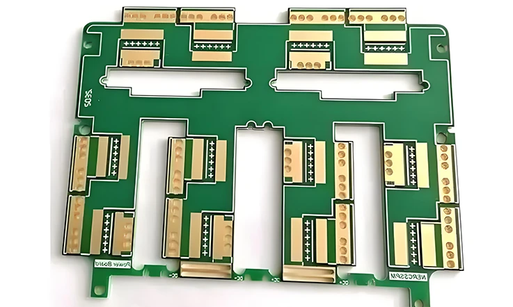
Taconic RF-60A PCB Manufacturing Services & Fabrication Capabilities

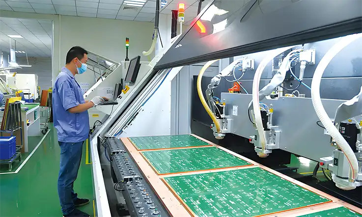
The manufacturing of Taconic RF-60A PCBs involves an intricate set of processes designed to maintain the integrity of high-frequency signals. These processes, from drilling and routing to surface finish selection and dimensional control, contribute to the overall performance of RF circuit boards. In this section, we dive deeper into these fabrication techniques, detailing how each step enhances the final product for use in RF and microwave applications.
Drilling, Routing, and Via Preparation for RF-60A Substrates
Manufacturing Taconic RF-60A PCBs involves specialized techniques for drilling, routing, and via preparation, which are all tailored to the needs of high-frequency designs. These processes ensure that the structure of the PCB remains stable and effective in supporting RF signals.
Drilling and Routing-
For RF-60A boards, precise drilling is needed to achieve clean and well-formed vias. This precision helps maintain the structural integrity of the PCB and limits parasitic effects that can disrupt signal transmission. CNC drilling systems ensure that vias are cleanly formed with minimal deviation, preventing defects that could impair performance in high-frequency designs.
Via Preparation-
When working with Taconic RF-60A materials, preparing vias is especially challenging due to the unique PTFE-based composition of the substrates. This composition can make traditional drilling methods less effective, so advanced methods such as laser drilling or mechanical drilling are often employed. This preparation ensures that vias are smooth and well-formed, minimizing the risk of poor copper plating that could affect signal quality.
For more complex designs, such as those requiring buried or blind vias, we must be precise in their alignment to ensure that no disruptions to the signal path occur. Every aspect of via preparation is closely controlled, from hole diameter to pad and trace dimensions, helping to ensure that the PCB remains well-suited to the high-frequency environment.
Surface Finishes: ENIG, Immersion Tin, and Gold Options
The choice of surface finish affects both the service life and electrical behavior of Taconic RF-60A PCBs, especially in terms of solder joint quality and high-frequency signal performance. Options such as ENIG, immersion tin, and gold plating each offer distinct characteristics that may be selected based on soldering method, environmental exposure, and frequency range.
ENIG (Electroless Nickel Immersion Gold)-
ENIG is a widely used surface finish for Taconic RF-60A PCBs, providing good corrosion resistance and solderability. The gold layer creates a smooth and flat surface that is ideal for soldering, while the nickel layer underneath offers added stability and durability. This finish also minimizes the potential for signal loss and reduces the risk of oxidation over time, making it a suitable choice for high-frequency applications.
Immersion Tin-
Another surface finish option is immersion tin, which is known for its cost-effectiveness and solderability. While immersion tin is a simpler finish than ENIG, it still delivers reliable performance in many RF applications. The flatness it provides is adequate for many designs, though it may not offer the same performance benefits at very high frequencies compared to more robust finishes like ENIG.
Gold Plating-
Gold plating is often selected for RF-60A PCBs when extra durability is needed. Gold offers superior resistance to oxidation and corrosion, providing long-lasting protection in demanding environments. In high-frequency applications where reliability is a top concern, gold plating ensures that the PCB maintains its quality over time, even in harsh conditions.
Tolerance Management and Dimensional Stability Control
Maintaining dimensional accuracy and stability is a core aspect of the Taconic RF-60A PCB manufacturing process. High-frequency applications demand precise control over the size and shape of each layer and via, as even slight variations can affect signal integrity.
Precision in Layer Alignment-
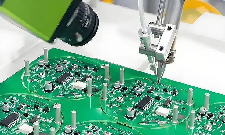
Multilayer PCBs require careful alignment to ensure that all copper layers are properly positioned. Any misalignment can lead to trace width or spacing issues, which can introduce impedance mismatches and signal degradation. Automated optical inspection (AOI) systems are used to monitor and correct any misalignment during the lamination process, ensuring that each layer is positioned with minimal deviation.
Dimensional Control for Stability-
For Taconic RF-60A substrates, consistent thickness—especially in heavier builds—directly affects impedance matching and overall signal behavior. During lamination, both temperature and pressure are maintained within specified ranges to help prevent uneven dielectric profiles, which may cause propagation delay or insertion loss shifts in high-frequency designs.
Final Inspection and Testing-
Before the finished RF-60A PCBs are shipped, they undergo comprehensive testing to ensure that they meet the necessary specifications. This testing includes impedance measurements at various points on the PCB, as well as visual inspections for any potential dimensional inconsistencies. This final round of checks guarantees that the PCBs will perform consistently and reliably in high-frequency applications.
Dimensional and Electrical Tolerances in Taconic RF-60A Manufacturing
The performance of RF and microwave printed circuit boards heavily depends on maintaining predictable electrical and dimensional stability throughout production. For PTFE-based Taconic RF-60A substrates, consistent processing ensures that these materials perform within specified margins, supporting designs operating across wide frequency bands. Below is an in-depth breakdown of process aspects that influence yield, reproducibility, and application fit.
Etching Precision and Trace Width Control
Maintaining accurate conductor geometries during subtractive etching has a direct influence on impedance performance. PTFE composites like RF-60A require close control during copper patterning to accommodate their low rigidity and dimensional expansion during thermal cycles.
●Tightly controlled trace width: Variation in trace width greater than ±0.01 mm can result in ±5% to ±8% deviation in target impedance at 2.4 GHz or 5.8 GHz applications.
●Photoresist adhesion and uniformity: High-frequency etch uniformity depends on resin-to-copper adhesion during photolithography.
●Edge profile control: Trapezoidal edge profiles can result in phase delay variation, especially across longer RF paths.
Consistent trace geometry isn’t just a process benefit—it reflects directly in impedance simulation accuracy. Avoiding over-etching is particularly useful when targeting antenna feedlines or directional coupler structures.
Etching Precision and Trace Width Control Data:
| Trace Width Variation (mm) | Impedance Deviation (%) | Frequency Range (GHz) |
| ±0.01 | ±5% to ±8% | 2.4 to 5.8 |
| ±0.02 | ±10% to ±15% | 2.4 to 5.8 |
| ±0.03 | ±15% to ±20% | 2.4 to 5.8 |
Dk/Df Consistency Across Batches
Dielectric constant (Dk) and dissipation factor (Df) stability are tracked through quality inspection and laminate lot certification. RF-60A typically maintains:
●Dk at 10 GHz: 6.15 ± 0.15 (IPC-TM-650 Method 2.5.5.5)
●Df at 10 GHz: 0.0027, providing relatively low insertion loss even on longer RF paths.
Batch-to-batch consistency affects filter and coupler tuning, and discrepancies in Dk can lead to shifts in resonance frequencies. For high-volume runs, it’s recommended to request material certification sheets from the laminate supplier to validate these ranges.
Dk/Df Consistency Across Batches Data:
| Frequency (GHz) | Dk Value | Df Value |
| 10 | 6.15 ± 0.15 | 0.0027 |
| 2.4 | 6.10 ± 0.10 | 0.0025 |
| 5.8 | 6.18 ± 0.12 | 0.0028 |
Lamination Repeatability and Flatness
Press cycle conditions—including heat ramp rate, peak temperature, and cooling method—directly impact flatness and interlayer alignment for multilayer RF-60A stackups. Repeatability in lamination ensures board-to-board uniformity, especially when blind and buried vias or cavity designs are involved.
●Typical flatness tolerance: Less than 0.1 mm bow/warp per 25 cm PCB length.
●CTE (Z-axis): 233 ppm/°C, which requires differential control when bonded with lower CTE prepregs or adjacent materials such as RO4450B.
●Bond film compatibility: TacBond 300 or compatible low-flow adhesives are typically selected for PTFE hybrid stackups.
Maintaining lamination flatness also reduces PCB assembly warpage and improves surface mount component placement on final RF modules.
Lamination Repeatability and Flatness Data:
| Parameter | Tolerance/Value |
| Flatness Tolerance | <0.1 mm bow/warp per 25 cm PCB length |
| CTE (Z-axis) | 233 ppm/°C |
| Bond Film Compatibility | TacBond 300 or compatible low-flow adhesives |
Standard Thicknesses and Copper Cladding for Taconic RF-60A PCBs
Taconic RF-60A laminates are selected across RF and microwave builds due to their balance of dielectric consistency, process stability, and copper compatibility. When designing with RF-60A, users often narrow their focus to a few preferred thicknesses and copper formats that suit application frequency, signal integrity, and manufacturing tolerance. This section outlines common substrate thicknesses, compares copper foil types, and touches on cladding techniques that align with various thermal and electrical goals.
25mil, 0.635mm, and Other Common Thickness Options
Taconic RF-60A substrates are manufactured in a range of thicknesses to accommodate various RF stackups and impedance requirements. Among them, 25mil (0.635mm) is widely applied in antenna arrays, power amplifiers, and signal distribution circuits. Common thickness options include:
●10mil (0.254mm) — Typically selected for narrowband filters and low-power microwave assemblies; contributes to tighter impedance control on microstrip lines.
●20mil (0.508mm) — Frequently used in power dividers and coupling networks; offers a balance between mechanical support and low insertion loss.
●25mil (0.635mm) — Regularly applied in 2-layer and 4-layer RF stackups; provides mechanical robustness with moderate insertion loss.
●60mil (1.524mm) — More suited for structural stiffness; appears in designs requiring mechanical rigidity under vibration or moderate thermal cycling.
All values conform to IPC-4101 tolerance classifications, and thickness uniformity is supported by the PTFE-glass construction of RF-60A.
Rolled Annealed vs Electrolytic Copper Types
Copper foil options directly affect etch resolution, conductor loss, and thermal cycling response in RF designs using RF-60A laminates. Two copper types are typically applied:
Rolled Annealed (RA) Copper-
●Smoother surface texture; supports better conductor loss performance above 10 GHz.
●Often preferred in stripline or edge-coupled designs where skin effect dominates.
●Enhances flexibility and ductility in flex-rigid or dynamic thermal environments.
Electrolytic (ED) Copper-
●Available in standard, low-profile (LP), and reverse-treated (RT) formats.
●Slightly rougher than RA copper; acceptable for microwave builds up to 6 GHz.
●More cost-effective and readily available in global fabrication networks.
The choice often depends on both circuit function and available fabrication processes, with RA favored in mmWave applications and ED copper chosen for mid-range RF and large-format antenna builds.
Foil Cladding Techniques and Thermal Considerations
Foil cladding defines how copper is bonded to the PTFE-based laminate and how thermal expansion is distributed across the circuit. With Taconic RF-60A, cladding options include:
Standard Foil Lamination-
●Utilizes high-pressure and temperature processes to anchor ED or RA copper to PTFE-glass.
●Supports layer-to-layer alignment and adhesion during multilayer lamination cycles.
●Can be optimized with oxide or plasma treatments to enhance bond strength.
Double-Treat Foil Options-
●Incorporates chemical surface prep to increase adhesion for fine-line circuits.
●Reduces copper delamination during reflow cycles.
Thermal Coefficient Matching-
●The low z-axis expansion of RF-60A pairs well with rolled copper in applications needing better dimensional control.
●Thermal conductivity (0.54 W/m·K) supports passive heat dissipation when RF output stages operate under continuous load.
For teams planning dense, high-power RF layouts or hybrid stackups with FR-4, cladding behavior under multiple lamination passes should be considered when defining prepreg selection and press cycle parameters.
Taconic RF-60A PCB Applications in Microwave and RF Systems
Taconic RF-60A laminates are engineered to meet the demands of high-frequency applications. Their consistent dielectric properties and mechanical stability make them suitable for various microwave and RF system applications. The following sections detail specific use cases across different industries.
5G Base Stations, GPS, and Antenna Boards
In commercial telecommunications, frequency stability and low loss are essential characteristics in material selection. Taconic RF-60A finds usage in:
●5G Base Stations: Applied in front-end modules and filter circuits, where consistent dielectric response helps maintain impedance over millimeter-wave frequencies.
●GPS Receiver Circuits: The low dissipation factor minimizes signal distortion across long signal chains.
●PCB-Based Antennas: The material supports planar antenna designs that must retain shape and performance across temperature shifts.
Many designers often choose RF-60A for systems where trace width, spacing, and return loss must be carefully managed to meet tight RF budgets.
Satellite Communication and Radar Module Integration
High-reliability sectors such as aerospace and defense employ Taconic RF-60A in:
●Satellite Uplink/Downlink Modules: Low moisture absorption helps preserve electrical properties in vacuum or high-humidity launch environments.
●Radar Front Ends: The PTFE composite allows routing of high-frequency signals with controlled impedance.
●Beamforming Networks: RF-60A helps maintain phase consistency across multiple feed lines used in phased array systems.
This material is often selected when repeatable performance under environmental and electrical load variations is required.
Automotive ADAS and IoT Device Usage
In transportation electronics and connected systems, the laminate’s balance of mechanical and RF properties fits with the following:
●ADAS Radar Boards: Applied in short-range radar modules operating at 24–77 GHz. Low signal attenuation supports clear detection resolution.
●IoT Gateways and Edge Devices: Used in RF links where space constraints and signal reliability are ongoing challenges.
●Infotainment Systems: Assists in maintaining clarity in RF audio and satellite input chains without introducing interference or drift.
Regulatory Compliance and Quality Assurance in RF-60A PCB Production
Taconic RF-60A-based PCBs are often deployed in fields where environmental regulations and performance consistency cannot be overlooked. This section outlines the specific standards, process checks, and documentation practices applied during fabrication, with the intent to support traceability, reliability, and conformity to commonly requested global directives.
RoHS and REACH Certification for Taconic RF-60A Laminates
Taconic RF-60A laminates meet both RoHS (Restriction of Hazardous Substances) and REACH (Registration, Evaluation, Authorization and Restriction of Chemicals) requirements. These frameworks are commonly requested by clients targeting markets with environmental compliance directives such as those in the EU or North America.
●RoHS-Compliant: Materials exclude banned substances like lead, cadmium, mercury, and hexavalent chromium.
●REACH Registration: Materials used in RF-60A laminates have been evaluated under the REACH regulation framework for chemical safety.
●Labeling & Documentation: Material declarations and safety data sheets are typically included in production files to streamline customer-side documentation and audit checks.
For those working in telecom infrastructure, aerospace platforms, or defense-grade systems, sourcing laminates aligned with these directives helps reduce friction during regulatory submission or third-party testing.
IPC Standards and RF QA Protocols
Several IPC guidelines are applied during the design, fabrication, and verification of Taconic RF-60A PCB builds. These standards ensure the mechanical, electrical, and material characteristics are aligned with common expectations in the RF and microwave industry.
●IPC-6018: Targets performance requirements for high-frequency printed boards, particularly for controlled impedance and dielectric consistency.
●IPC-2228: Guides engineers through RF-specific PCB layout strategies, especially where hybrid stackups or mixed dielectric layers are used.
●IPC-4103: Defines base material specifications, such as PTFE-based laminates, used in RF and high-speed digital applications.
By applying these protocols, we can reduce variation and simplify tuning processes during circuit tuning and qualification.
Traceability, Outgassing, and Thermal Cycle Reliability
Manufacturing RF-60A-based boards for defense, aerospace, or satellite usage often involves additional checks related to stability, emissions, and long-term durability under extreme conditions.
●Traceability: Each lot of RF-60A laminate is tagged with lot numbers, press cycle identifiers, and drill/mill parameters. This helps backtrack material usage in case of requalification or customer-side audit.
●Outgassing: According to ASTM E595, RF-60A shows low volatile content:
– TML: 0.02%
– CVCM: 0.00%
– WVR: 0.01%
These figures make the material suitable for vacuum systems or space-grade platforms where gas release could interfere with optics or sensors.
●Thermal Cycling: With a Z-axis CTE of 69 ppm/°C (from -30°C to 125°C), RF-60A can be used in environments where repeated temperature swings are part of daily operation, such as phased array radar or outdoor 5G equipment.
Taconic RF-60A PCB vs Rogers RO4350B & Other RF Substrates
Taconic RF-60A and Rogers RO4350B are two widely used materials in RF/microwave PCB fabrication. Both serve in multilayer circuits for telecommunications, automotive electronics, radar, and network infrastructure. They differ in dielectric properties, thermal stability, cost, and availability, which affects selection decisions depending on layout constraints, frequency targets, and material compatibility in stackups.
Electrical and Mechanical Property Comparison
The decision between RF-60A and RO4350B often begins with a review of core electrical parameters and how each laminate responds to mechanical and thermal stress over time. Below are comparative benchmarks based on published datasheets and processing feedback from fabrication environments:
●Dielectric Constant (Dk) @10GHz
– Taconic RF-60A: 6.15 ±0.15
– Rogers RO4350B: ~3.48 ±0.05
RF-60A may be better suited in designs where higher impedance control or tighter trace spacing is required in compact RF structures.
●Dissipation Factor (Df) @10GHz
– RF-60A: 0.0025
– RO4350B: 0.0037
Lower Df values generally support lower transmission losses, particularly on long trace runs or high-power applications.
●Z-axis CTE (ppm/°C)
– RF-60A: 24
– RO4350B: 46
Lower CTE values contribute to improved via reliability in thermally cycled assemblies.
●Peel Strength (1 oz Cu after solder float)
– Both materials support strong copper-to-dielectric adhesion with pre-cleaning and standard oxide treatment.
In multi-GHz systems, these parameters influence insertion loss, phase delay, and impedance matching. RF-60A offers tighter control over Dk at the cost of increased handling care during processing, while RO4350B balances ease of fabrication with moderate dielectric performance.
Cost and Availability in Global Markets
Pricing and logistics influence PCB stackup choices, especially in programs requiring regional supply chain optimization or high-volume repeat runs.
●Material Cost per ft² (general range):
– RF-60A is often positioned as a cost-effective high-Dk PTFE laminate
– RO4350B pricing tends to be more stable in volume, but subject to fixed-tier pricing models from authorized distributors.
●Regional Availability:
– RO4350B is more commonly stocked in North America and Western Europe.
– RF-60A may be more readily sourced in Asia-Pacific, especially for high-mix, low-volume runs.
●Panel Size and Custom Sheet Options:
– RF-60A offers greater flexibility in custom dimensions for non-standard tooling setups.
– RO4350B generally ships in standard panel sizes, facilitating large-batch production.
Procurement teams should confirm current lead times across multiple vendors before finalizing their stackup selections. Local distributor support and backup sourcing options also affect material selection strategy.
Compatibility with Hybrid Stackups and Bonding Films
Our engineers often integrate RF-60A or RO4350B into hybrid constructions involving thermoset layers or FR-4, which requires close matching of thermal and mechanical properties across all materials.
●Bonding Film Usage:
–RF-60A pairs with Taconic fast-cure epoxy or thermoset bonding films (e.g., FR-27)
–These films work with both PTFE and non-PTFE layers to support RF and control layers in the same stackup.
●Sequential Lamination Compatibility:
–RF-60A maintains dimensional stability during multiple lamination cycles, minimizing interlayer shift or bubble formation.
●CTE Compatibility:
–With low z-axis expansion, RF-60A reduces risk of cracked vias when combined with FR-4 or hydrocarbon layers.
●Surface Conditioning:
–Pre-bonding surface prep (e.g., plasma cleaning or mechanical scrubbing) enhances lamination quality with RF-60A cores.
Hybrid constructions are common in applications requiring a mix of analog and digital layers or low-pass filter integration. RF-60A supports stable interlayer bonding and process predictability across diverse lamination cycles.
How to Get a Quote for Taconic RF-60A PCB Manufacturing Services from JarnisTech?
Obtaining a quote for Taconic RF-60A PCB manufacturing services involves a straightforward process aimed at aligning your specific needs with our production capabilities. At JarnisTech, we prioritize a transparent quoting process that takes into account your design specifications, production volume, and delivery timelines. Here’s how you can easily get started with a quote request.
Upload Gerber or ODB++ Files for DFM Analysis
To ensure a seamless process, you can upload your Gerber or ODB++ files directly to our platform for a detailed Design for Manufacturability (DFM) analysis. This step allows us to review your design for any potential production challenges related to trace width, via size, or layer stackup configuration. We check that the design fits within the capabilities of Taconic RF-60A substrates, and make adjustments to optimize production efficiency.
●DFM Benefits: Early identification of issues can help reduce redesigns and minimize production delays.
●File Requirements: We accept both Gerber files and ODB++ formats. The more comprehensive your files, the better our analysis.
Table 1: Common DFM Issues and Their Solutions
| Issue | Description | Solution |
| Trace Width Variations | Differences in trace width can affect impedance | Adjust trace width within tolerances of ±0.01 mm |
| Via Size Inconsistencies | Mis-sized vias can cause poor electrical contacts | Ensure via dimensions meet design specs |
| Layer Stackup Errors | Misalignment of layers can cause shorts or opens | Review layer stackup and interlayer alignment |
By submitting your design files for DFM, you are ensuring that your project will be reviewed with precision, making sure that it is feasible and cost-effective to produce.
Lead Time, Pricing, and MOQ Details
Understanding the lead time, pricing, and minimum order quantities (MOQ) helps with organizing production timelines and estimating project expenses. At JarnisTech, we tailor our quotes based on these factors:
●Lead Time: Our standard lead times for Taconic RF-60A PCBs range from 10 to 15 business days, depending on complexity and volume. Rush orders can be expedited with prior arrangements.
●Pricing Structure: Pricing varies based on the board complexity, dimensions, and any additional processes such as surface finishes or special testing requirements. Bulk orders can benefit from price breaks.
●MOQ: Our minimum order quantity for Taconic RF-60A PCBs is generally 50 units. However, smaller runs are also feasible depending on the project’s requirements.
Table 2: Lead Time and MOQ Details
| Factor | Standard Range | Custom Orders |
| Lead Time | 10-15 business days | Expedite available upon request |
| Pricing | Based on complexity and size | Bulk pricing available |
| Minimum Order Quantity | 50 units | Small batches possible on request |
When reaching out for a quote, be sure to specify the quantity and urgency of your order so we can provide the most accurate and tailored pricing for your needs.
Global Shipping and Export Support
At JarnisTech, we are committed to delivering your finished RF-60A PCBs to locations across North America, Europe, Asia, and beyond. Our logistics team coordinates efficient shipping and manages all required export documentation. We provide multiple delivery options tailored to fit your project timeline and budget.
●Shipping Options: Standard, expedited, and express services are available based on your required delivery date.
●Export Support: We assist with export regulations, customs paperwork, and tracking to ensure that your PCBs reach you without delays.
Table 3: Shipping and Export Details
| Region | Shipping Options | Estimated Delivery Time |
| North America | Standard, Expedited, Express | 5-7 business days |
| Europe | Standard, Expedited | 7-10 business days |
| Asia | Standard, Expedited, Express | 5-8 business days |
| International | Standard, Expedited | 10-15 business days |
Ready to get started? Send over your files for analysis and request a personalized quote today. Our team is ready to provide you with a cost-effective and efficient solution for your Taconic RF-60A PCB needs.
Taconic RF-60A PCB (FAQ)
1.What are the advantages of using Taconic RF-60A for multilayer designs?
RF-60A maintains its excellent electrical performance across multilayer designs, providing uniform signal integrity and low-loss characteristics.
2.Can Taconic RF-60A be used in applications requiring high thermal cycling resistance?
Yes, RF-60A offers good thermal cycling stability, making it suitable for applications subject to frequent temperature fluctuations.
3.What are the typical applications for Taconic RF-60A in the telecommunications industry?
RF-60A is commonly used in high-frequency components such as filters, antennas, and microwave amplifiers within telecommunications.
4.What is the maximum frequency range supported by Taconic RF-60A?
Taconic RF-60A performs well at frequencies up to 40 GHz, making it suitable for most RF and microwave applications.


