
In modern high-reliability electronics, the long-term stability of a printed circuit board (PCB) is defined less by its glass transition temperature (Tg) in isolation, and more by the material’s capacity to manage Z-axis thermal expansion (CTE) under cyclic thermal stress. The Nanya NPG151 laminate is engineered for this specific challenge. Its foundational strength is an advanced resin system formulated to suppress Z-axis expansion. This attribute fundamentally mitigates primary failure mechanisms in complex assemblies: stress fatigue and barrel cracking in plated through-holes (PTH) during temperature shock events.
Turning this material science advantage into a defect-free result requires a deep understanding of its behavior during fabrication. This guide focuses on the interaction between resin properties, advanced Design for Manufacturability (DFM), and controlled processing techniques. It outlines how to adjust lamination cycles to support the fill of heavy copper areas often found in electric vehicle (EV) builds, how careful prepreg selection supports smooth, void-free surfaces for HDI and System-in-Package (SiP) designs, and how the material’s characteristics can be applied to preserve signal performance in 5G and AI circuit applications. This resource serves as a structured approach to applying NPG151 effectively in advanced board manufacturing.
Technical Summary:
1.Superior thermomechanical stability driven by a low Z-axis CTE (under 3.0% at 260°C), directly mitigating plated-through-hole (PTH) failures in thick or high-layer-count boards.
2.Enables high-yield fabrication of complex HDI and ELIC structures through exceptional dimensional stability across multiple sequential lamination cycles.
3.Provides a reliable platform for high-speed digital and RF applications due to stable dielectric properties (Dk4.3–4.5, Df <0.015 @ 1GHz). 4.High glass transition temperature (Tg>170°C) furnishes a robust processing window for demanding lead-free assembly and rework profiles.
5.Full process compatibility with advanced thermal management solutions, including heavy copper planes and embedded coin technology.
Unpacking NPG151: Core Thermomechanical and Electrical Properties
The foundation of any reliable multilayer PCB is its core material. Nanya NPG151 provides the dimensional stability, electrical integrity, and thermal endurance needed to survive complex fabrication cycles and to function in harsh operational environments. This section consolidates its performance attributes that directly elevate board quality, yield, and long-term dependability.
Unmatched Thermomechanical Stability
A material’s behavior under thermal stress dictates its structural integrity. NPG151 is engineered to perform where conventional materials may falter.
●Exceptional Dimensional Stability: With a low coefficient of thermal expansion, especially in the critical Z-axis (under 3.0% at 260°C), NPG151 maintains superior layer-to-layer registration and effectively controls warpage during lamination and subsequent high-temperature assembly steps. This quality is foundational for high-layer-count and HDI boards.
●High Glass Transition Temperature (Tg): A typical Tg exceeding 170°C furnishes a generous process window for multiple lead-free soldering cycles, press-fit connector installations, and conformal coating cures without material degradation.
●Robust Chemical and Heat Resistance: The epoxy resin system is formulated to withstand aggressive cleaning agents and demanding soldering profiles, preserving the electrical insulation and mechanical structure of the finished board throughout its lifecycle.
Table: Thermomechanical Performance of Nanya NPG151
| Property | NPG151 Performance |
| Z-axis CTE (at 260°C) | < 3.0% |
| Glass Transition Temperature (Tg) | > 170°C |
| Chemical Resistance | Excellent – compatible with aggressive cleaning agents |
| Heat Resistance | High – maintains structure in high-temp soldering |
High-Performance Electrical Characteristics
In high-speed and high-frequency designs, stable and predictable electrical properties are non-negotiable for achieving target performance.
●Stable Dielectric Constant (Dk): With a Dk value consistently in the 4.3–4.5 range across a wide frequency band, NPG151 serves as a reliable foundation for controlled impedance modeling, a necessity for differential pairs, microstrip, and stripline trace geometries.
●Low Dissipation Factor (Df): The material’s low Df (typically under 0.015 @ 1GHz) minimizes insertion loss, preserving the integrity of high-speed digital signals. This makes it highly suitable for applications such as automotive radar, 5G infrastructure, and medical imaging signal chains operating in the 1–10 GHz range.
●High Dielectric Breakdown Voltage: NPG151 provides excellent electrical insulation, a defining factor for preventing shorts in high-voltage power applications and ensuring safety in medical and industrial equipment.
Table: Electrical Properties of Nanya NPG151
| Property | NPG151 Performance |
| Dielectric Constant (Dk) | 4.3–4.5 (1–10 GHz range) |
| Dissipation Factor (Df) | < 0.015 @ 1GHz |
| Dielectric Breakdown Voltage | High – effective insulation under high voltage |
| Frequency Stability | Stable across GHz-range frequencies |
A Comparative Analysis: NPG151 vs. Alternative Materials
Selecting the appropriate laminate is a foundational design decision. Here is a direct comparison between NPG151 and other common materials, illustrating its distinct advantages under different technical and processing conditions.
●Versus Standard FR-4: NPG151’s significantly lower Z-axis CTE and higher Tg drastically reduce internal board stress during thermal cycling. This directly translates to higher PTH reliability and a lower propensity for warpage compared to standard FR-4, making it the superior choice for any multilayer board requiring long-term dependability.
●Versus High-Tg FR-4: While many materials have a high Tg, NPG151 combines this with superior dimensional stability and a lower CTE. It better preserves the structural integrity of solder joints and microvias through repeated reflow cycles, offering a more robust overall solution.
●Versus BT (Bismaleimide-Triazine): While BT offers excellent thermal properties, NPG151 provides a more cost-effective solution with comparable performance for many high-reliability applications, along with easier integration into standard FR-4 processing workflows.
●Versus Polyimide: NPG151 offers a process advantage over polyimide, which often requires specialized handling, extended curing cycles, and presents adhesion challenges. NPG151 delivers high-reliability performance without the associated manufacturing complexity and cost.
Table: Material Comparison Overview
| Material | Z-axis CTE | Tg (°C) | Processing Complexity | Cost Efficiency |
| Standard FR-4 | Typically > 4.5% | 130–140°C | Low | High |
| High-Tg FR-4 | 3.5–4.0% | 150–170°C | Moderate | Moderate |
| BT (Bismaleimide-Triazine) | 2.5–3.0% | > 200°C | High | High |
| Polyimide | 2.0–2.5% | > 250°C | Very High | Low |
| Nanya NPG151 | < 3.0% | > 170°C | Moderate | Moderate to High |
DFM for NPG151: Designing for Manufacturability and Reliability
Designing with Nanya NPG151 is not just about schematic and layout; it involves proactively engineering for manufacturability. The following DFM guidelines are intended to leverage the material’s full potential and achieve high-yield, mechanically stable outcomes.
Foundational Stackup Design for Mechanical Integrity
A structurally sound stackup is the blueprint for a board that remains flat and reliable after enduring the extreme stresses of lamination and reflow.
1.Symmetry and Balance:
A symmetric stackup is a prerequisite for flatness. This includes mirroring the layer count, copper distribution, and dielectric thickness above and below the board’s centerline. A balanced design is the most effective method against the internal stresses that cause bow and twist.
2.Unified Grain Direction:
For maximum dimensional stability, the grain direction of all cores and prepregs should be aligned. This practice minimizes anisotropic shrinkage during cooling, a primary cause of warpage. This information is available on supplier datasheets and must be followed during layup.
3.Matching Resin to Copper Density:
For inner layers with heavy copper features (e.g., 2 oz or greater), the selection of prepregs with sufficient resin content and flow (e.g., 1080 or 2116 styles) ensures complete encapsulation of traces and planes. This prevents resin starvation, a common cause of delamination and internal voids.
4.Copper Thieving and Balancing:
On sparse layers positioned opposite denser ones, adding non-functional copper patterns (thieving) helps even out copper distribution across the panel. This supports more uniform pressure during lamination, contributes to stable thickness control, and reduces the chance of localized warping.
Engineering Robust Vias and Interconnect Structures
NPG151’s low-CTE resin system provides a stable foundation for vias, but robust design practices are still needed to guarantee interconnect reliability.
1.Through-Hole Aspect Ratios:
For reliable plating and structural integrity, the aspect ratio (board thickness divided by drill diameter) must be managed. For a typical 1.6 mm thick board, maintaining hole diameters of 0.2 mm or larger (an aspect ratio of 8:1) is advisable. Higher aspect ratios demand specialized drilling and plating processes.
2.Microvia Structures in HDI:
The material’s stability supports stacked microvia designs (e.g., up to 3 levels). For maximum mechanical resilience against thermal and physical stress, however, a staggered microvia configuration is generally recommended as it distributes stress more effectively.
3.Via-in-Pad Best Practices:
While NPG151’s controlled-flow resin helps minimize voiding, via-in-pad designs require stringent process control. Pads must be sufficiently large to accommodate the via and its annular ring. Specifications should demand that vias be filled and capped to ensure a solderable, flat surface for component mounting.
4.Annular Ring and Teardrops:
A sufficient annular ring is needed to guarantee a strong connection between the via barrel and the copper trace. For fine-pitch BGA breakouts or thin traces, adding teardrops where traces meet pads enhances mechanical strength and reduces the risk of broken connections.
DFM Checklist Summary:
●Is the proposed stackup symmetric in terms of layer count and copper weight?
●Is the grain direction of all core and prepreg materials specified to be unified?
●Have high-flow prepregs (e.g., 1080, 2116) been selected for layers with heavy (≥ 2oz) or dense copper features?
●Are annular rings sufficient for all drill sizes according to IPC standards?
●Have teardrops been applied to traces connecting to fine-pitch or high-stress pads?
Mastering the Process: Assembly and Lamination Guidelines for NPG151
Mastering the lamination process for NPG151 is where its potential is unlocked. The balance of resin flow, copper topography, pressure, and temperature determines final yield, registration, and reliability. These guidelines are derived from extensive practical application.
Precision Control of the Lamination Cycle
A precisely calibrated lamination cycle is the foundation of a high-quality multilayer board.
●Strategic Heating Rate Control: A controlled thermal ramp rate of 1.5–2.5°C per minute is maintained in the gelation phase (70°C to 140°C). A ramp that is too fast can trap moisture and trigger uneven resin flow, leading to voids or delamination.
●Full Resin Cure Duration: To ensure complete polymer cross-linking, the material must be held at a temperature above 170°C for a minimum of 60 minutes. An incomplete cure results in reduced thermal performance and increased Z-axis expansion.
●Controlled Cooling and Pressure Release: During the cool-down phase, a press pressure of under 100 PSI is maintained until the board temperature drops below 100°C. Releasing pressure too early can induce significant internal stress and compromise layer-to-layer registration.
●Material Preparation and Handling: To prevent delamination from moisture absorption, all materials must be stored in a climate-controlled environment (20°C / 50% RH). A pre-lamination bake cycle for inner layer cores is strongly recommended for high-reliability applications.
Table: Recommended Lamination Parameters for NPG151
| Parameter | Recommended Value |
| Heating Rate (70°C–140°C) | 1.5–2.5°C/min |
| Cure Temperature | ≥ 170°C |
| Cure Time | ≥ 60 minutes |
| Cooling Pressure Maintenance Temp | Until < 100°C |
| Press Pressure | ≤ 100 PSI |
| Material Storage Conditions | 20°C ±2°C / 50% ±5% RH |
| Pre-bake Time for Inner Layers | 4–6 hours @ 105°C |
Optimizing Drilling, Desmear, and Plating Processes
The quality of a drilled and plated hole is a direct indicator of manufacturing precision and a predictor of long-term reliability.
●Optimized Drilling Parameters: The filled resin system of NPG151 requires optimized drill parameters. The use of sharp, high-quality carbide drills with appropriate chip loads and speeds prevents resin smear and hole wall damage.
●Effective Desmear Process: After drilling, a three-step desmear process (solvent, permanganate, and neutralizer) removes any resin smear from inner layer copper interconnects, ensuring a clean surface for plating adhesion.
●High-Throw Plating for Aspect Ratios: Boards with high aspect ratio through-holes require a plating process with high “throwing power.” This ensures a uniform deposition of copper down the entire length of the via barrel, a frequent failure point under thermal stress.
Table: Drilling and Plating Guidelines for NPG151
| Process Step | Recommended Practice |
| Drill Tooling | Sharp, coated carbide drills; adjusted chip load |
| Entry/Exit Materials | Rigid entry / composite exit stackups |
| Desmear Procedure | Solvent → Permanganate → Neutralizer |
| Aspect Ratio (Preferred) | ≤ 10:1 (Higher may require advanced plating chemistries) |
| Plating Method | High-throw acid copper process with via fill compatibility |
Lamination Process Checklist Summary:
●Are all materials (cores and prepregs) properly stored and baked to control moisture content before layup?
●Is the lamination press programmed for a controlled heating rate of 1.5–2.5°C/minute in the 70-140°C range?
●Does the cycle ensure a full cure at >170°C for a minimum of 60 minutes?
●Is pressure maintained during the cool-down cycle until the material is below 100°C?
●Is a multi-step desmear process specified in the routing after drilling and before plating?
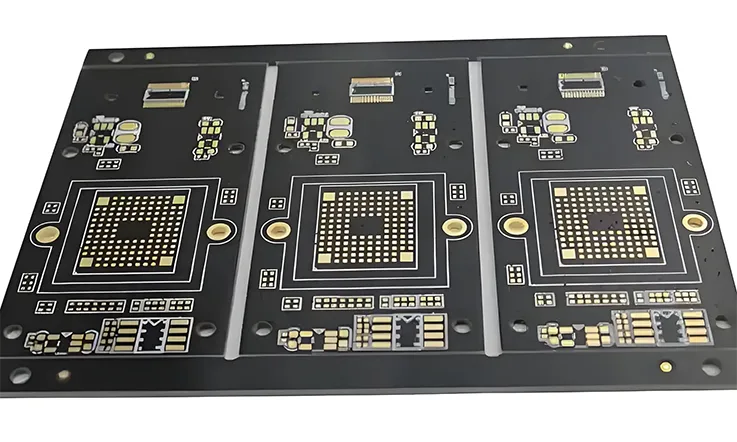
Pushing the Limits: Fabricating Advanced HDI and ELIC Structures with NPG151
The drive toward miniaturization and increased functionality has made High-Density Interconnect (HDI) and Any-Layer Interconnect (ELIC) technologies indispensable. These structures, characterized by multiple layers of stacked and staggered microvias, subject the base material to extreme processing stress. The exceptional dimensional stability of Nanya NPG151 makes it a reliable choice for these applications, enabling designs that are not feasible with conventional materials.
The Sequential Lamination Challenge in HDI Manufacturing
HDI and ELIC boards are constructed through sequential lamination, where layers are added and processed in multiple stages.
●The Challenge of Registration: Each lamination cycle involves high temperature and pressure. Without a dimensionally stable material, layer-to-layer registration becomes compromised. The predictable shrinkage characteristics of NPG151 allow engineers to precisely compensate for material movement at each stage.
●NPG151’s Function: The low in-plane (X, Y) CTE of NPG151 ensures that a laser-drilled microvia on layer 10 aligns perfectly with its target pad on layer 9, even after 8 or more press cycles. This predictability is a requirement for achieving high yields in complex HDI fabrication.
Achieving Clean Laser Ablation for High-Quality Microvias
Microvias are typically formed by lasers. The interaction between the laser and the laminate is a demanding process step.
●Laser Ablation Characteristics: The NPG151 resin system is engineered for clean laser ablation. The material’s composition minimizes carbon residue, a condition for reliable via bottom contact.
●Controlling Via Shape and Quality: Laser parameters (pulse energy, duration, beam focus) are precisely controlled to create an ideal via shape with a slight taper. This “champagne flute” shape facilitates superior copper plating and a robust connection.
Building Reliable Stacked Microvia Interconnects
Stacked microvias represent the pinnacle of HDI technology and also the greatest reliability challenge.
●The “Weak Knee” Problem: During thermal cycling, immense stress is put on the point where one via connects to the next. If the via is not perfectly filled, this point can fracture.
●NPG151’s Contribution to a Strong Stack: The dimensional stability of NPG151 provides a solid foundation. Its smooth drilled-hole wall quality promotes excellent adhesion for the via-fill and plating processes, creating a solid, contiguous copper structure that can withstand thousands of thermal cycles.
The Critical Interface: Selecting the Optimal Surface Finish
The surface finish is the interface between the PCB and the components assembled onto it. The choice of finish has profound implications for solderability, signal integrity, reliability, and cost. For a high-performance material like NPG151, selecting an appropriate surface finish is a determinant in preserving the integrity of the final assembly.
ENIG (Electroless Nickel Immersion Gold): The All-Rounder
ENIG is a popular choice for its excellent planarity, good solderability, and suitability for aluminum wire bonding.
●Advantages on NPG151: The stable surface of NPG151 provides an ideal substrate for the electroless nickel deposition process, ensuring a uniform, well-adhered nickel layer.
●Mitigating “Black Pad” Risk: “Black pad” is a potential failure mode in the ENIG process. Tightly controlled plating chemistry and process times, combined with NPG151’s material integrity, effectively eliminate the factors that lead to this defect.
Immersion Silver (ImAg): The Choice for Signal Integrity
For high-frequency applications, Immersion Silver offers outstanding electrical performance.
●Signal Integrity Benefits: Silver is an excellent conductor with minimal impact on high-speed signals, making ImAg a good choice for RF and microwave circuits built on NPG151.
●Process and Handling Considerations: Immersion Silver’s primary challenge is its susceptibility to tarnishing. The application of advanced anti-tarnish agents and specialized, vacuum-sealed packaging protects the boards until assembly.
Immersion Tin (ImSn): Planarity for Press-Fit and Soldering
Immersion Tin is another planar finish that offers excellent solderability, making it a strong candidate for press-fit applications.
●Performance on NPG151: The smooth surface of NPG151 allows for a uniform and consistent deposition of Immersion Tin.
●Managing Tin Whisker Concerns: Modern Immersion Tin processes utilize specific grain structures and post-process treatments that significantly inhibit whisker formation.
OSP (Organic Solderability Preservative): The Economical, Planar Option
OSP is a cost-effective, environmentally friendly option that provides a very planar surface.
●Use Case with NPG151: For high-volume, cost-sensitive applications that do not require numerous reflow cycles, OSP can be an effective choice.
●Limitations: OSP is less robust than metallic finishes and is typically consumed after one or two reflow cycles. For high-reliability boards, a more robust metallic finish like ENIG or ImAg is generally specified.
Advanced Thermal Management Strategies and Solutions
As power densities increase in applications like EV powertrains and 5G base stations, thermal management becomes a central design challenge. The inherent properties of NPG151 make it an excellent platform for implementing advanced cooling strategies.
Deploying Thermal Vias for Efficient Heat Dissipation
Thermal vias are a highly effective method for transferring heat from a component on the surface to internal or external copper planes.
●Design and Placement: A dense array of thermal vias is placed directly under the thermal pads of hot components. For maximum effectiveness, they should be filled with thermally conductive epoxy.
●Optimizing Via Size and Density: A larger number of smaller vias (e.g., 0.3 mm) is often more effective than a few large vias. NPG151’s stability ensures the integrity of these dense via fields.
●Connecting to Thermal Planes: The thermal vias must connect to large, solid copper planes. The low Z-axis CTE of NPG151 minimizes stress on these connections during thermal cycling.
Table: Thermal Via Implementation Guidelines
| Design Aspect | Recommendation |
| Via Hole Diameter | 0.25 mm – 0.35 mm |
| Via Pitch (Dense Array) | 0.6 mm – 1.0 mm |
| Filling Material | Thermally conductive epoxy (≥3 W/m·K) |
| Via Type | Through-hole or via-in-pad (filled and capped) |
| Connection | Solid copper thermal plane (top or inner) |
| Z-axis CTE (NPG151) | < 3.0% at 260°C |
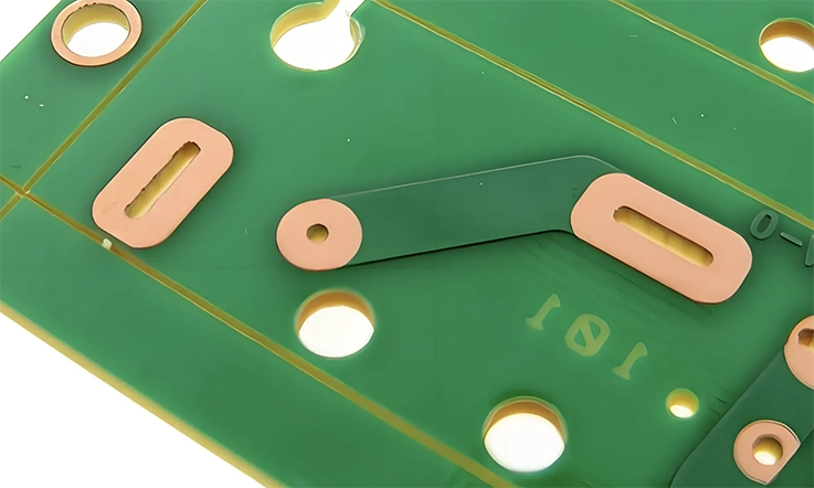
Implementing Heavy Copper and Embedded Coin Technologies
For extreme power applications, more aggressive thermal solutions are required. The robust nature of NPG151 supports these advanced structures.
●Heavy Copper Traces and Planes: NPG151 can be reliably fabricated with heavy copper layers (3 oz, 4 oz, or more). The main fabrication challenge is ensuring complete resin fill around these thick features.
●Embedded Copper Coin Technology: For localized hotspots, a solid copper coin can be embedded directly into a cutout in the PCB, providing a direct thermal path to a heatsink. The predictable resin flow of NPG151 is a requisite for achieving a void-free bond around the coin.
Table: Heavy Copper & Coin Integration Parameters
| Parameter | Specification |
| Heavy Copper Thickness | 3 oz – 6 oz (105 – 210 µm) |
| Minimum Spacing (Copper–Copper) | ≥ 0.2 mm with filled resin |
| Coin Material | Pure copper (≥99.9%) |
| Coin Integration Depth | Partial or full-depth cutout |
| Resin Fill Requirement | Void-free around edges (pressure-assisted lamination) |
| Prepreg Style Recommendation | 2116 or 7628 for controlled resin content |
Ensuring Signal Integrity in High-Speed and RF Designs
In systems operating at gigahertz frequencies, the PCB is no longer a simple interconnect but a complex component that influences signal behavior. The electrical properties of NPG151 provide a stable starting point, but expert design and fabrication are required to maintain signal integrity.
Achieving Precise and Consistent Impedance Control
Maintaining a constant impedance is a requirement for preventing signal reflections.
●Modeling and Material Characterization: Advanced field solvers and empirical data are used to accurately model trace geometries needed to achieve target impedances (e.g., 50Ω single-ended, 100Ω differential).
●Process Control for Consistency: Achieving tight impedance control (e.g., ±5%) requires precise control over the final dielectric thickness and trace width etching.
Mitigating the Glass Weave Effect in Multi-Gigahertz Systems
The periodic structure of the woven glass fabric can cause signal skew at multi-gigahertz frequencies.
●Strategic Material Selection: For sensitive layers, prepregs that use mechanically spread or flat-weave glass styles (e.g., 1067, 1080) are recommended to create a more uniform dielectric medium.
●Advanced Routing Techniques: High-speed differential pairs can be routed at a slight angle (e.g., 3-5 degrees) relative to the glass weave direction to minimize intra-pair skew.
Design Techniques for Minimizing Insertion Loss and Crosstalk
For a signal to arrive cleanly, loss and noise must be minimized.
●Low-Profile Copper Foils: For RF and high-speed digital layers, low-profile (LP) or very-low-profile (VLP) copper foils are paired with NPG151 to reduce conductor losses from the skin effect.
●Trace Spacing and Grounding: Proper spacing between traces minimizes crosstalk. Solid ground planes and strategically placed stitching vias provide a clean return path for signals.
A Commitment to Quality: In-Process Control for Zero-Defect Production
A superior material like NPG151 only reaches its full potential when processed under a rigorous quality control regime. Quality is not a final inspection step; it is a philosophy embedded in every stage of fabrication. This commitment to in-process control is how an excellent design becomes a zero-defect, high-reliability physical product.
The Foundation: Front-End Engineering and Material Traceability
Quality begins before the first sheet of laminate is cut.
●Comprehensive DFM Analysis: Every design undergoes an exhaustive Design for Manufacturability (DFM) review. CAM engineers simulate the entire fabrication process, identifying potential issues like acid traps or solder mask slivers before they can cause problems.
●Complete Material Traceability: A strict barcode-based traceability system is implemented. Every panel is linked to the specific batches of core, prepreg, and copper foil used in its construction.
Eyes on Every Layer: AOI and AXI In-Process Inspection
Catching defects early maintains high yields and ensures final quality.
●Automated Optical Inspection (AOI): After etching, every inner and outer layer is scanned by high-resolution AOI systems, identifying any defects such as opens, shorts, or incorrect trace widths with micron-level precision.
●Automated X-Ray Inspection (AXI): After lamination, AXI is used to see inside the board. This non-destructive technique verifies layer-to-layer registration with extreme accuracy.
The Final Proof: Electrical Testing and Microsection Analysis
Final verification provides objective proof that the board meets all specifications.
●100% Electrical Testing: Every board undergoes a “flying probe” or “bed-of-nails” electrical test, checking for continuity and isolation across the entire netlist.
●Time Domain Reflectometry (TDR) for Impedance Control: Test coupons fabricated alongside production panels are tested using a TDR to provide customers with documented proof that impedance requirements have been met.
●Destructive Physical Analysis (Microsectioning): As the ultimate proof of quality, cross-sectional analysis is routinely performed. Under a high-power microscope, inspectors check for PTH plating thickness, via fill integrity, and absence of delamination.
Verifying Endurance: Qualification and Long-Term Reliability Testing
High-reliability is not a claim; it is a verifiable attribute. The performance of NPG151 assemblies is validated through rigorous testing, providing the assurance needed for mission-application devices.
Assessing Conductive Anodic Filament (CAF) Resistance
CAF is an electrochemical failure mode causing shorts between vias or traces.
●Material and Process Factors: The NPG151 resin system and clean processing create a strong bond between the resin and glass fibers. This robust interface is highly resistant to CAF formation.
●Design for CAF Prevention: Design rules, such as maintaining minimum hole-to-hole spacing, further reduce the risk of CAF.
Simulating a Lifetime of Stress: Interconnect Stress Testing (IST)
IST is a method of accelerated reliability testing where the board is subjected to rapid thermal cycles.
●Verifying PTH and Microvia Reliability: IST is used to validate the thermomechanical robustness of NPG151 assemblies. The low Z-axis CTE of NPG151 consistently demonstrates superior performance in IST, showing minimal resistance increase.
Surviving the Extremes: Thermal Shock and Cycling Tests
This testing validates a board’s ability to withstand extreme temperature swings.
●Test Profile: A typical test involves rapidly transferring the assembly between extreme cold (-40°C) and hot (+125°C or higher) for hundreds or thousands of cycles.
●NPG151 Performance: NPG151 boards exhibit exceptional resistance to pad cratering, solder joint fatigue, and via barrel cracking during these tests.
Proven in the Field: Application-Specific Use Cases
NPG151 provides a dependable material platform for electronics across demanding sectors. Its balanced profile addresses the unique challenges of each.
Medical Devices: Ensuring Sterilization Resistance and Biocompatibility
Medical boards place extreme demands on a material’s chemical safety and stability.
●Withstanding Sterilization Cycles: The high Tg (>170°C) and excellent moisture resistance of NPG151 make it well-suited for devices that undergo multiple autoclave or vapor sterilization cycles.
●Chemically Safe Formulation: Its halogen-free, antimony-free, and red phosphorous-free composition reduces the risk of outgassing, making it a strong choice where biocompatibility is a consideration.
●Structural Stability for Miniaturized Designs: In compact medical analyzers or implantable devices, the material’s low Z-axis expansion protects delicate via structures.
Automotive Systems: Delivering Reliability Under Harsh Conditions
Automotive electronics must function for years while subjected to extreme temperature swings and constant vibration.
●Resilience to Thermal Fatigue: The NPG151 resin system controls thermal expansion effectively across wide temperature deltas (e.g., -40°C to +125°C), reducing mechanical stress on PTHs and solder joints.
●Support for High-Density Control Modules: In space-constrained ECUs, BMS, or ADAS modules, the material’s dimensional stability provides a dependable foundation for high-density layouts.
●Compatibility with Lead-Free Assembly: A high Tg provides the necessary processing window for the aggressive, multi-reflow soldering profiles required for modern automotive assemblies.
Industrial & 5G Infrastructure: Built for Endurance and Performance
Industrial boards require decades of operation, while 5G systems demand stable performance at high frequencies.
●Stable Dielectric Performance: NPG151 maintains its dielectric properties at higher operational voltages, making it suitable for servo motor controllers or power inverters.
●Mechanical Soundness for Large-Format Boards: When grain alignment practices are followed, the material exhibits low warpage, an advantage for the large-format panels used in power distribution systems.
●Flexible Cost-Performance Configurations: The availability of various prepreg glass styles allows designers to optimize the stackup for mechanical strength, resin fill, or cost.
Post-Assembly Considerations: Conformal Coating and Rework
The performance of the base material extends beyond board fabrication into the final assembly (PCBA) lifecycle.
●Conformal Coating Compatibility: The stable surface energy and chemical resistance of NPG151 ensure excellent adhesion with all common types of conformal coatings, including acrylic, silicone, and urethane. This provides a reliable, long-term barrier against moisture and contaminants for the final assembled board.
●Rework Resilience: The material’s high decomposition temperature (Td) and high Tg furnish a robust capacity to withstand the localized heat stress of rework operations. This allows for the safe removal and replacement of complex components like BGAs without inducing substrate delamination, blistering, or pad lift—a defining feature for high-value assemblies.
Technical Specifications and Compliance Verifications
A laminate’s specified chemistry and its associated verifications are foundational to its behavior during assembly and its long-term reliability. The specified chemistry and international approvals for Nanya NPG151 provide assurance for demanding electronics.
Environmentally Conscious Chemistry and Global Compliance
The design of NPG151 addresses environmental directives and operator safety. It is formulated without halogens, antimony, or red phosphorous.
●Safer Processing Environments: This chemistry markedly reduces the emission of toxic gases during thermal events.
●Improved Circuit Reliability: The halogen-free composition lowers the risk of corrosive residues that can impair the long-term function of a circuit.
●Verification of Global Compliance: NPG151 adheres to RoHS and REACH directives, ensuring boards can meet global market access requirements.
Adherence to International Performance and Safety Standards
The material’s behavior is defined by established industry benchmarks.
●Adherence to Performance Specifications: The material conforms to IPC-4101E (L127/128). This specification sets internationally recognized parameters for electrical, thermal, and mechanical properties.
●Fire Safety Verification: Its flammability rating meets the UL 94 V-0 classification and is confirmed under UL File E98983.
Navigating Commercials: Cost, Sourcing, and Supply Chain
Strategic planning for projects using Nanya NPG151 requires a comprehensive view of material choices, design complexity, and sourcing cycles. Aligning design specifications with assembly capabilities at the project’s outset is foundational to managing costs and ensuring supply stability.
Understanding the Drivers of Final Board Cost
The final cost of a board using NPG151 is shaped less by the raw material price and more by how the design affects the fabrication process.
●Heavy Copper and Resin Consumption: Designs with 2 oz or thicker inner-layer copper require more prepreg with high-flow characteristics for complete encapsulation.
●Overhead for Fine-Line or Impedance Control: Tight tolerances add to the CAM engineering workload and can lower panel yield if not carefully optimized.
●Complexity of Stackup Design: Using multiple, dissimilar prepreg glass styles within a single stackup can complicate the lamination press cycle.
Proactive Planning for Lead Times and Minimum Orders
Effective project scheduling requires foresight into the supply variations of different NPG151 configurations.
●MOQs for Specific Prepreg Styles: Less common prepreg configurations may be subject to longer replenishment intervals or higher minimum order quantities.
●Lead Time Variation by Copper Foil: While 0.5 oz and 1 oz copper foils are generally available, constructions requiring 2 oz inner layers may need a forecast of 3–4 weeks or more.
●Extended Cycles for Custom Stackups: If a project involves a non-standard build, the availability of all specified laminates should be confirmed during the design stage.
OEM Strategies for Lifecycle and Supply Risk Management
For long-lifecycle products, material selection must be validated for both performance and multi-year supply viability.
●Long-Term Planning with IPC Standards: Compliance with IPC-4101E (L127/128) provides a stable specification basis for qualification planning.
●Designing for Supply Chain Resilience: To mitigate risks, it is prudent to design and qualify an alternate stackup using more common prepreg substitutes.
●Using Buffer Stock for Demand Fluctuations: For high-volume programs, establishing a buffer stock of the specified laminate can help manage shared material demand.
Expert Support for NPG151 Projects
Bringing a Nanya NPG151 project to completion requires that board design and assembly methods work in close coordination. From resin behavior during lamination to copper distribution and drill performance, effective communication between layout engineers and board assembly personnel shapes the final outcome. For both early-stage prototypes and scaled system builds, having access to process details ahead of time can help reduce delays and avoid unnecessary revisions.
Request a Quote or Working Sample for Evaluation
Evaluating whether Nanya NPG151 suits the board requirements can begin with an informed cost estimate or a hands-on review of physical boards built with the material.
●Receive Comparative Quotes: Obtain cost comparisons across multiple stackup combinations, such as 4-layer, 6-layer, and 8-layer builds with various copper weights.
●Request Working Samples: A direct way to validate through-hole integrity, silkscreen adhesion, and surface finish quality before committing to a larger build.
●Match Requirements to Proven Configurations: Benefit from access to established stackups that have already passed qualification in medical, EV, or industrial applications.
Access Stackup Design and DFM Consultation
To use NPG151 effectively in complex designs—especially those with impedance control or mixed-dielectric constructions—stackup planning must align with actual process behaviors, not just datasheet values.
●Review of Prepreg Selection and Copper Balance: Access guidance on glass styles, resin flow potential, and copper balancing, which is especially useful when managing large ground planes or dense via fields.
●Analysis of Lamination Effects: For builds involving multiple press cycles or blind/buried vias, a simulation of Z-axis expansion and resin bleed at each stage can be provided.
●Guidance on Drilling and Aspect Ratios: Align drill-back tolerances and via aspect ratio plans with the specified inner-layer copper thickness to ensure mechanical strength and signal integrity.
Obtain Technical and Compliance Files
For internal compliance reviews or material traceability in regulated builds, structured technical references can simplify the qualification process.
●Complete IPC-4101E Specifications: Full conformance data for L127/L128 to assist with OEM board audits or quality reviews.
●Detailed Lamination and Pressing Profiles: Available files include recommended pressing rates, hold times, and cooling slopes for NPG151.
●Compliance and Safety Data: UL recognition data and RoHS/REACH status summaries can be prepared to match customer submission formats for large system contracts.
Frequently Asked Questions (FAQ)
1.Can NPG151 be used in a hybrid stackup with RF materials like Rogers or Taconic?
Yes. It is frequently used for digital or power layers in hybrid constructions. This requires precise lamination process control to manage the different thermal expansion properties.
2.Is the glass weave effect of NPG151 a concern for signals above 10GHz?
Yes, this is a characteristic of all woven-glass laminates. To mitigate the effect, using mechanically spread or flat-weave glass styles (e.g., 1080, 1067) and employing design techniques like rotated routing are recommended.
3.How does the cost of NPG151 compare to other high-Tg FR-4 materials?
It is positioned as a high-performance, cost-effective option. It offers certain thermal properties approaching more specialized materials but remains competitively priced against other high-performance FR-4 laminates.
4.How does NPG151 perform regarding outgassing in a vacuum?
It has low outgassing properties suitable for many vacuum environments but is not rated to NASA standards. For space-grade applications, specific testing per ASTM E595 would be required.
Glossary of Terms
●AOI (Automated Optical Inspection): An automated machine vision inspection of a printed circuit board for manufacturing defects such as shorts, opens, or incorrect component placement.
●AXI (Automated X-Ray Inspection): A technology used to inspect the internal layers and solder joints of a PCB, especially for BGA components and layer registration.
●CAF (Conductive Anodic Filament): An electrochemical failure mode involving the growth of a conductive filament along the resin/glass fiber interface within the PCB substrate.
●CTE (Coefficient of Thermal Expansion): The measure of a material’s tendency to change in shape, area, and volume when exposed to temperature variation. Z-axis CTE influences how well vias maintain structural integrity under thermal cycling.
●DFM (Design for Manufacturability): The practice of designing products in a way that makes them easy and efficient to manufacture.
●ELIC (Every Layer Interconnect): An advanced HDI design where each layer has laser-drilled microvias, allowing for maximum routing density.
●HDI (High-Density Interconnect): A type of PCB with a higher wiring density per unit area than conventional boards, characterized by fine lines/spaces, microvias, and high-performance thin materials.
●IST (Interconnect Stress Testing): An accelerated reliability test that subjects a PCB coupon to rapid thermal cycles to induce failures and assess the thermomechanical reliability of the interconnect structures.
●PCBA (Printed Circuit Board Assembly): A PCB with all the electronic components soldered onto it.
●PTH (Plated Through-Hole): A hole in a PCB that is plated with copper and connects copper traces from one layer of the board to others.
●TDR (Time Domain Reflectometry): A measurement technique used to determine the characteristics of electrical lines by observing reflected waveforms. It is used to verify the impedance of traces on a PCB.
Referenced Standards
●IPC-4101E: Specification for Base Materials for Rigid and Multilayer Printed Boards.
●UL 94: The Standard for Safety of Flammability of Plastic Materials for Parts in Devices and Appliances.
●ASTM E595: Standard Test Method for Total Mass Loss and Collected Volatile Condensable Materials from Outgassing in a Vacuum Environment.


