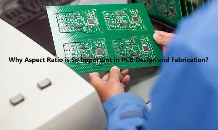
This is the ideal resource if you are seeking expert guidance on the aspect ratio of printed circuit boards (PCBs).
The aspect ratio is a vital concern in the design of PCBs, as it affects both the functionality and manufacturability of the board. High aspect ratios may impede the drilling of holes or production of vias, potentially compromising the overall performance of the board. Conversely, low aspect ratios may restrict the number of components that can be placed on the board.
In this article, we will provide a detailed explanation of PCB aspect ratios, including their significance in PCB fabrication. Please read on for a comprehensive overview.
What is Aspect Ratio in PCB Design ?
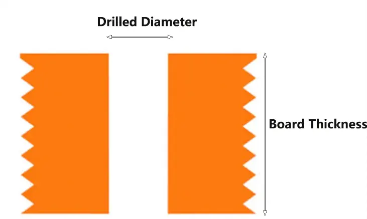
The aspect ratio in PCB design refers to the ratio of a printed circuit board’s thickness to the diameter of its drilled holes. In other words, it is the relationship between the drilled hole size and the thickness of the board material.
Aspect ratio is an important consideration in PCB design because it can affect the PCB’s reliability, manufacturability, and performance. High aspect ratios, where the ratio of the drilled hole diameter to board thickness is larger, can be more challenging to produce reliably and cost-effectively. Therefore, it is essential to carefully design PCBs with appropriate aspect ratios to achieve desired performance and functionality while also ensuring manufacturability.
Importance of Aspect Ratio in PCB Design
The aspect ratio is an essential consideration in PCB design because it can impact several aspects of the PCB’s performance and manufacturability. Here are a few reasons why aspect ratio is important in PCB design:
● Reliability: PCBs with an inappropriate aspect ratio can lead to reliability issues such as breakage or delamination during processing or in the field.
● Signal integrity: High aspect ratio PCBs can cause impedance mismatches, signal attenuation, and other problems that can degrade signal integrity.
● Manufacturability: PCBs with high aspect ratios can be more challenging to manufacture, especially in terms of drilling small holes.
● Cost: High aspect ratio PCBs are generally more costly to produce due to the added complexity and potential for errors during manufacturing.
● Space constraints: A PCB with a larger aspect ratio can allow for greater trace density while still maintaining clearance spacing, which is especially important for miniaturized electronics where space is limited.
As a result, selecting an appropriate aspect ratio for a PCB design is crucial to achieving desired performance, reliability, and manufacturability while also minimizing costs and maximizing use of space.
How Do You Calculate PCB Aspect Ratio ?
Calculating the aspect ratio of PCB vias is of utmost importance, regardless of whether you are creating an image, a video, or any other creative work. Typically, statistical methods are employed to determine the specifications of this calculator. The aspect ratio is the ratio that establishes how high graphic objects, pictures, or films should be and how wide they must be. It can be found in the formula for aspect ratio.
Although various aspect ratios may be available for height and length dimensions, the ratio value is typically scaled down to the lowest acceptable ratio that suitably accommodates all types of media.
Here are a few ways in which aspect ratio could be utilized in PCB:
As a PCB manufacturer, we understand that the aspect ratio is a crucial characteristic in the production of printed circuit boards.
● In the first example, a board thickness of 62 mils and a hole diameter of 31 mils result in an aspect ratio of 2:1.
● The second example achieves an aspect ratio of 8:1 through a board thickness of 64 mils and a drilled hole width of eight mils.
● The third scenario involves a board thickness of 80 mils, producing an aspect ratio of 10:1, and utilizing a drilled hole diameter of eight mils.
It is important to note that a higher aspect ratio leads to a greater need for plating, which in turn increases the risk of cracking due to expansion during the PCB assembly phase. Therefore, to promote stronger vias and improved electrical connections, lowering the aspect ratio is necessary. A lower PCB aspect ratio ensures more consistent plating throughout the vias, which contributes to a higher level of durability throughout the entire lifespan of the printed circuit board.
JarnisTech Capabilities of NC Drilling Vias
| Min NC Drilling Via Diameter | Available Aspect Ratio | Max Available PCB Thickness |
| 0.15mm | <=8:1 | 1.2mm |
| 0.20mm | <=10:1 | 2.0mm |
| 0.25mm | <=12:1 | 3.0mm |
JarnisTech Capabilities of Laser Ablated Microvias
| Smallest Laser Microvia | 3mil (0.075mm) |
| Largest Laser Microvia | 10mil (0.25mm) |
| Microvia Aspect Ratio | Standard: 0.75:1 Advanced: 1:1 |
| Capture Pad Size | Standard: μVia +0.008 Advanced: μVia +0.006 |
| Land Pad Size | Standard: μVia + 8mil Advanced: μVia + 6mil |
| Stacked Microvia | Yes |
| Type I Capabilities | Yes |
| Type II Capabilities | Yes |
| Type III Capabilities | Design Dependent |
| Copper Filled Microvias | Yes |
For through-hole vias, an AR 8:1 maximum is recommended, as stated by the design guidelines found in the IPC-2221A and IPC-222 documents. A minimum drill diameter of 0.20 millimeters is recommended for use with a standard PCB thickness of 1.60 mm. At JarnisTech, however, we can achieve a density of 10:1 and 12:1 for through-hole boards, as well as a density of 0.75:1 and 1:1 for microvia HDI PCBs.
These parameters are highly suggested by JarnisTech and are completely appropriate for use in PCB manufacturing. In order to meet the high dependability standards of IPC Class 3, requirements like these are necessary. It is not possible to unilaterally reduce the size of the via pad or the hole diameter since there are considerations related to reliability.
Factors Influencing PCB Aspect Ratio
Printed circuit boards (PCBs) are a crucial component in many electronic devices, providing a base for the mounting of various electrical parts. During the design and fabrication of PCBs, careful consideration must be given to the aspect ratio of the board as it can significantly impact the performance and reliability of the final product. In this section, we will explore the various factors that influence aspect ratio and their impact on the PCB design and manufacturing.
● Density and Size of Components: The size and density of components on a printed circuit board (PCB) can also have an impact on its aspect ratio. A greater density of smaller surface mount technology (SMT) components on a PCB can lead to less expansive aspect ratios. Conversely, using larger through-hole components necessitates larger vias and holes, which may limit the aspect ratio.
The component density on a PCB can also influence the aspect ratio. High-density printed circuit boards (PCBs) contain numerous components in a small area, necessitating smaller holes and vias. This can result in less desirable aspect ratios since the thickness of the PCB places a constraint on the depth of holes or vias.
● PCB Layer Count and Thickness: The aspect ratio of a printed circuit board (PCB) is primarily influenced by its thickness and layer count. Calculating the aspect ratio of a PCB involves dividing its thickness by the smallest hole’s diameter. As the PCB thickness increases, its aspect ratio reduces, and vice versa.
The layer count of a PCB can also impact its aspect ratio, with multi-layer PCBs typically featuring lower ratios. These PCBs possess more than two layers of conductive material that sandwich insulating layers, which limit the maximum drill depth achievable in the holes or vias.
● PCB Fabrication Process Capabilities: The manufacturing process utilized in making a PCB can also impact its aspect ratio significantly. Different manufacturing techniques offer varying capabilities when it comes to creating PCBs with varying aspect ratios. For instance, the drilling and plating process used to create holes or vias on a printed circuit board (PCB) can impact its aspect ratio.
Typically, mechanical or laser drilling is employed by PCB manufacturer to create holes or vias on a PCB. Mechanical drilling is utilized for larger holes and vias, whereas laser drilling is used for smaller ones, resulting in reduced diameter holes and vias and subsequently smaller aspect ratios.
The plating method used to generate the conductive layer within the holes or vias also has an influence on the aspect ratio. Electroless plating is the preferred choice for smaller holes and vias, while electroplating is employed for larger holes and vias. Electroless plating provides a more uniform and consistent plating layer within the hole or via, which can lead to a higher aspect ratio.
How the Aspect Ratio Affects the Design and Manufacturing of PCBs ?
The aspect ratio of a printed circuit board (PCB) affects both its design and production process. A larger aspect ratio allows for deeper holes or vias, which can increase the device’s mechanical stability and thermal efficiency, resulting in a more reliable and sturdy design. However, a high aspect ratio can make the manufacturing process more challenging, requiring greater precision during drilling and plating operations.
Producing PCBs with a high aspect ratio can be a time-consuming and costly process. Achieving high-quality holes and vias requires additional effort during drilling and plating, potentially leading to higher fault rates and lower yields. This can increase production costs and extend lead times.
Therefore, it is necessary to carefully consider the aspect ratio and its potential impact on the production process during PCB design. Appropriate design adjustments can help to balance the aspect ratio with the production feasibility, ensuring that the aspect ratio is conducive to the PCB’s normal production.
So, How to ensure that the aspect ratio is conducive to the normal production of PCB ?
● Communication with the Manufacturer: To ensure effective PCB manufacturing, it is crucial to maintain open communication with the manufacturer throughout the design process. This enables early identification of any manufacturing concerns and facilitates design revisions that can improve the product’s manufacturability.
Furthermore, it is important to have a comprehensive understanding of the manufacturer’s capabilities and constraints in designing printed circuit boards (PCBs). PCB manufacturers’ capabilities may vary in terms of aspect ratios, making it necessary to select a manufacturer capable of meeting the design specifications.
Designers must also consider the tolerances and requirements necessary for the holes and vias on the PCB to ensure the desired aspect ratio.
Additionally, designers should rely on design guidelines and principles to ensure that the PCB design meets the minimum criteria for drilling and plating. Such guidelines can prevent common manufacturing problems, including breakout and burrs. Maintaining open communication with the PCB manufacturer and following design principles can help achieve efficient and effective PCB manufacturing.
Impact of Aspect Ratio on PCB performance
The impact of aspect ratio on PCB performance includes:
● Signal Losses: Higher aspect ratio vias may have increased parasitic capacitance and inductance, leading to higher signal losses and decreased signal quality.
● Electrical Reliability: High aspect ratio vias may have insufficient plating thicknesses leading to open circuits, decrease in reliability or electrical performance degradation.
● Thermal Management: High aspect ratio vias impede the flow of heat in a PCB, which can lead to thermal management problems such as hot spots, uneven temperature distribution, and decreased reliability of components.
● Manufacturability: The aspect ratio of a via can impact manufacturability, which can affect the yield, cost, and production speed of PCB manufacturing.
● Design Flexibility: Low aspect ratio vias offer more design flexibility which can be preferable in some situations, but high aspect ratio vias are needed for some designs where a larger distance must be covered between layers.
Therefore, the aspect ratio of vias is an important consideration in PCB design and has a significant impact on both electrical performance and manufacturability of printed circuit boards.
Challenges in Achieving High Aspect Ratio
Achieving high aspect ratios in PCB design can be challenging due to a number of factors, such as:
● Drilling limitations: Drilling small holes with high aspect ratios can cause drill bits to break or wear out quickly, increasing the risk of errors and inaccuracies in the PCB design.
● Plating issues: Plating the inside of small, high aspect ratio holes with copper can be difficult, leading to incomplete plating or voids that may affect the performance of the PCB.
● Lamination challenges: Getting the copper layers to adhere properly during the lamination process can be tricky when dealing with very thin traces and tight spaces between them.
● Etching difficulties: Etching small, high aspect ratio traces can be difficult because the acid doesn’t always flow evenly into the narrow spaces.
● Signal integrity: High aspect ratios can create impedance mismatches, signal attenuation, and other problems that can degrade signal integrity.
Advanced Techniques for Maintaining Aspect Ratio
here are several advanced techniques for maintaining aspect ratio in high-density PCB designs:
● Laser drilling: Laser technology allows for precise drilling of small holes with high aspect ratios, which can minimize breaking or wearing of drill bits and reduce errors in the PCB.
● Sequential lamination: In this process, the laminate material is built up one layer at a time, allowing for more precise control of the thickness of each layer and ensuring better adhesion of the copper layers.
● Resin-coated copper (RCC): RCC is a process in which a resin coating is applied to the copper layer before drilling to provide reinforcement and prevent delamination.
● Plasma etching: Instead of using traditional acid etching, plasma etching employs charged gas molecules to create a highly controlled and more uniform process for etching small, high aspect ratio traces.
● Staggered drilling: Staggered drilling involves drilling holes in alternating locations in adjacent layers, which can reduce the aspect ratio by allowing for larger holes to be drilled in some layers.
By using these advanced techniques, it is possible to achieve the high aspect ratios necessary for miniaturized, high-density PCB designs while also maintaining high levels of performance, reliability, and manufacturability.
How to Choose the Right Aspect Ratio for Your PCB Design ?
Choosing the right aspect ratio for your PCB design involves several factors, including the size and complexity of the board, the number and size of components, and the performance and cost requirements of the final product. Here are a few steps to help you choose the appropriate aspect ratio for your PCB design:
Determine the size of the board and the number and size of components that will be used. This will help you determine the general thickness of the PCB.
Consider the pitch between components on the board and any other spacing requirements. This will help you determine the minimum drill size.
Check with your PCB manufacturer to determine their capabilities for drilling and plating small holes with high aspect ratios.
Calculate the required aspect ratio by dividing the board thickness by the minimum drill size. The recommended aspect ratio is typically between 8:1 and 12:1 to ensure proper plating and adhesion.
Consider any signal integrity issues that may arise with high aspect ratio designs. For high-speed applications, it may be necessary to adjust the aspect ratio to ensure proper signal integrity.
By carefully considering these factors and working closely with your PCB manufacturer, you can select an appropriate aspect ratio for your PCB design that balances performance, reliability, and manufacturability.
Summary
Aspect ratio is an essential consideration in PCB design as it influences the manufacturability, reliability, and performance of the printed circuit board. The aspect ratio of a PCB represents the relationship between its thickness and the diameter of its drilled holes, and choosing the right aspect ratio involves balancing numerous factors such as the size, complexity, and intended use of the PCB. Advanced techniques such as laser drilling, sequential lamination, RCC, plasma etching, and staggered drilling can help to overcome the challenges associated with high aspect ratio designs. Therefore, designers must carefully consider aspect ratio when developing PCB designs to ensure efficient and effective manufacturing, reliable performance, and optimal use of space.
PCB manufacturers considering reducing the aspect ratio of their circuit boards must keep in mind the board thickness and minimum drill diameter. Failing to do so can lead to manufacturing roadblocks and delays. Lowering the aspect ratio can result in stronger vias and larger connection areas for components.
JarnisTech, a reputable PCB manufacturer, offers a vast selection of capabilities and specifications due to over 20 years of experience serving customers in a range of industries. Our commitment to providing high-quality PCBs at affordable prices has earned us a prominent position in the industry. Our turnaround times are among the fastest in the market. Interested customers can contact us to learn more about the various types of PCBs that we offer.