
The design of a printed circuit board (PCB) stack-up plays a crucial role in the overall performance and functionality of electronic devices. A 4-layer PCB stack-up offers numerous advantages in terms of design flexibility, signal integrity, power distribution, and space optimization. This article provides a comprehensive overview of the considerations and benefits associated with 4-layer PCB stack-ups.
In the following sections, we will explore the different options for arranging layers, discuss the key considerations for thermal management, and highlight the significant advantages that a 4-layer PCB stack-up can offer. Understanding these aspects will empower designers to make informed decisions and optimize their designs for efficient and reliable operation.
What is 4-layer PCB Stackup?
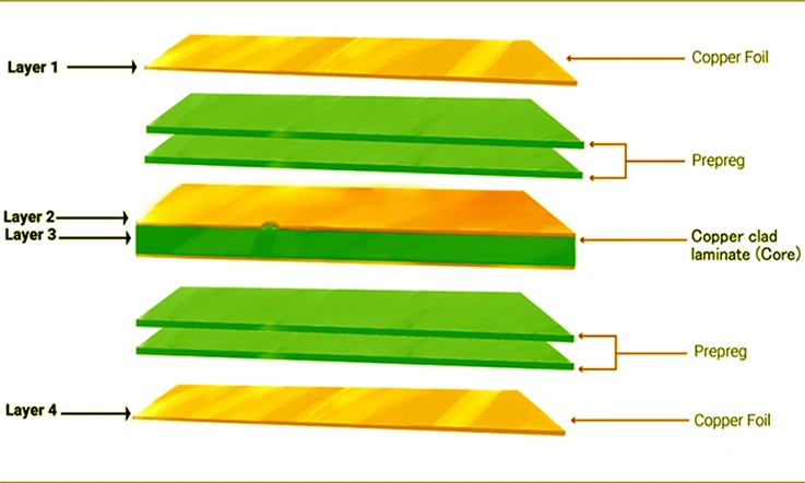
A 4-layer PCB configuration comprises four distinct layers: a top layer, a bottom layer, and two inner layers. Among these layers, two are dedicated to carrying signals, with one serving as a VCC (power supply) layer and the other as a GND (ground) layer.
Traditionally, the inner layers of a 4-layer PCB are utilized as power and ground planes to ensure effective distribution of power and stability of the reference voltage. By incorporating power and GND planes within the inner layers, electromagnetic emissions are minimized, thus enhancing the overall signal quality and robustness of the PCB design.
In terms of routing and component placement, the outer layers play a pivotal role. They are responsible for accommodating signal traces as well as providing adequate space for the strategic positioning of electronic components. The outer layers facilitate efficient routing of signals while considering factors such as signal integrity, impedance control, and noise immunity.
The allocation of the inner layers as power and GND planes in a 4-layer PCB offers notable advantages. By establishing low-inductance current paths and minimizing the loop area, potential EMI issues can be mitigated, leading to improved performance and reliability. Additionally, the presence of dedicated power and GND planes ensures stable power distribution, reduces noise susceptibility, and helps maintain a solid reference potential across the circuit.
Layers of 4-Layer Stack-up PCB
In a typical 4-layer stack-up PCB configuration, the layers are organized in the following order:
Top Layer: Positioned as the outermost layer of the PCB, the top layer accommodates components like SMDs, connectors, and other circuit elements. Its primary function is to route signals and traces, enabling the interconnection of components and facilitating signal flow.
Internal Signal Layer: Situated below the top layer, the first internal signal layer serves as an additional routing layer for signals and traces. Compared to lower-layer stack-ups, this layer offers increased routing options and flexibility, contributing to efficient signal routing and optimized circuit design.
Internal Power or Ground Plane: Found between the two internal signal layers, the internal power or ground plane plays a crucial role. It functions as a conductive layer responsible for carrying either the power supply voltage or serving as a reference ground. By providing a low-impedance path for power distribution, this plane helps minimize noise and electromagnetic interference, enhancing signal integrity and overall performance.
Bottom Layer: Positioned at the bottommost part of the PCB, the bottom layer serves as an additional routing layer. It facilitates the connection of components and completes the circuit paths, further enabling the flow of signals and traces.
The layer arrangement in a 4-layer stack-up PCB delivers several advantages. The inclusion of dedicated power and ground planes enhances signal integrity by minimizing noise and providing stable power distribution. These planes also help reduce electromagnetic interference, contributing to better overall performance and reliability of the PCB design.
Different Options for Arranging the Layers in a 4-layer PCB Stack-up
There are different options for arranging the layers in a 4-layer PCB stack-up. Here are a few common layer arrangements:
Signal – Ground – Power – Signal:
Top Layer: Signal routing and components
Second Layer: Ground plane
Third Layer: Power plane
Bottom Layer: Signal routing and components
Signal – Power – Ground – Signal:
Top Layer: Signal routing and components
Second Layer: Power plane
Third Layer: Ground plane
Bottom Layer: Signal routing and components
Ground – Signal – Signal – Power:
Top Layer: Ground plane
Second Layer: Signal routing and components
Third Layer: Signal routing and components
Bottom Layer: Power plane
Power – Signal – Ground – Signal:
Top Layer: Power plane
Second Layer: Signal routing and components
Third Layer: Ground plane
Bottom Layer: Signal routing and components
Signal – Ground – Signal – Power:
Top Layer: Signal routing and components
Second Layer: Ground plane
Third Layer: Signal routing and components
Bottom Layer: Power plane
Note that the specific layer arrangement depends on the design requirements, including signal integrity, power delivery, and thermal management. The decision may also be influenced by factors such as EMI/EMC considerations, component placement, and ease of manufacturing. It is crucial to carefully analyze and evaluate the particular project’s needs to choose the most suitable layer arrangement for a 4-layer PCB stack-up.
4-Layer PCB Stackup Thickness
Layer PCBs offer two options for the thickness of core and prepreg materials. The standard thickness is typically 1.6 mm (approximately 0.06 in), although 1.2 mm (about 0.05 in) is commonly used as well.
In a 1.6 mm (about 0.06 in) thick PCB, the core material occupies a thickness of 1.2 mm (about 0.05 in), while two prepregs are utilized, each with a thickness of 0.2 mm (about 0.01 in).
Alternatively, for a 1.2 mm (about 0.05 in) thick PCB, the core material is reduced to 0.8 mm (about 0.03 in), with one prepreg layer of 0.2 mm (about 0.01 in) containing a coil, and another prepreg layer of 0.2 mm (about 0.01 in) containing copper.
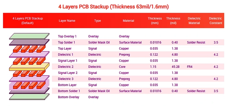
This differentiation in core and prepreg thicknesses allows for flexibility in the design and fabrication of 4-layer PCBs. Engineers can select the appropriate thickness based on specific design requirements, such as space constraints, signal integrity considerations, and mechanical strength. The choice of core and prepreg thicknesses plays a crucial role in achieving the desired electrical and mechanical performance of the PCB.
Benefits of 4 Layer PCB Stack-Up
There are several benefits associated with using a 4-layer PCB stack-up:
Increased Design Flexibility:
With four layers, engineers have more routing options and can achieve higher density designs. The additional layers provide greater freedom for signal routing, power distribution, and component placement, allowing for more complex and advanced circuit designs.
Enhanced Signal Integrity:
The multiple layers in a 4-layer PCB allow for better signal integrity. Separating power and ground layers from signal layers helps minimize noise and reduces the likelihood of signal interference, improving overall signal quality and reducing the risk of electromagnetic interference (EMI).
Efficient Power Distribution:
The dedicated power and ground planes in the internal layers of a 4-layer PCB provide consistent and stable power distribution. These planes help minimize voltage drops, control impedance, and reduce the chances of power-related issues, resulting in improved performance and reduced power noise.
Small Form Factor and Space Savings:
4-layer PCBs enable higher component density and compact designs, making them suitable for space-constrained applications. By utilizing multiple layers, circuit complexity can be increased while maintaining a relatively small physical footprint, which is essential for miniaturized electronic devices.
Cost Optimization:
Compared to higher layer count PCBs, such as 6 or 8 layers, designing and manufacturing a 4-layer PCB typically offers cost advantages. Fewer layers mean simpler manufacturing processes, reduced material costs, and shorter development cycles. It can be a cost-effective solution for many applications without compromising functionality and performance.
Improved Thermal Management:
When designing a 4-layer PCB, it is possible to allocate specific layers as thermal planes, allowing for efficient heat dissipation. By separating heat-generating components from critical signal traces, the PCB’s thermal performance can be optimized, resulting in improved reliability and reduced susceptibility to thermal issues.
Overall, the benefits of a 4-layer PCB stack-up include increased design flexibility, enhanced signal integrity, efficient power distribution, space savings, cost optimization, and improved thermal management. These advantages make 4-layer PCBs a popular choice for a wide range of electronic applications, from consumer electronics and telecommunications to industrial equipment and medical devices.
Considerations Associated with 4-Layer Stack-ups
When designing a 4-layer PCB stack-up, there are several important considerations to keep in mind:
Signal Integrity:
Ensure that signal traces have controlled impedance and minimal signal degradation. Proper placement and routing of traces, as well as appropriate layer selection, can help maintain signal integrity and reduce the risk of crosstalk and noise.
Power and Ground Planes:
Allocate dedicated power and ground planes in the inner layers to achieve stable power distribution, reduce noise, and provide a solid reference potential for signals. Proper placement and connectivity of these planes are critical for minimizing voltage drops and ensuring effective grounding.
Layer Arrangement:
Decide on the optimal layer arrangement based on specific design requirements. Consider factors like the complexity of the circuit, the need for controlled impedance, ease of routing, and thermal management. The order of layers, such as signal layers, power/ground planes, and reference planes, plays a significant role in achieving desired performance.
Thermal Considerations:
Adequate thermal management is crucial to prevent overheating of components. Allocate copper planes for heat dissipation and ensure sufficient spacing between components to allow for proper airflow. Proper choice of materials and consideration of thermal vias can help in efficient heat dissipation.
Manufacturing Constraints:
Understand the capabilities of the manufacturing process and select stack-up configurations that are compatible with the chosen fabrication technologies. Consider factors such as minimum track width, minimum via sizes, and material availability to ensure feasibility and cost-efficiency of the manufacturing process.
EMI/EMC:
Minimize electromagnetic interference (EMI) by controlling the layer stack-up and routing practices. Proper placement of power and ground planes, careful signal routing, and appropriate use of decoupling capacitors and shielding techniques can help reduce EMI and ensure compliance with electromagnetic compatibility (EMC) standards.
Design for Assembly and Serviceability:
Consider ease of assembly and future servicing requirements when deciding on the layer stack-up. Ensure accessibility to components, proper clearance and spacing for assembly tools, and ease of rework or repair if needed.
Cost Optimization:
Evaluate the design requirements and determine the most cost-effective stack-up configuration that meets the desired performance. Consider factors like material costs, manufacturing complexities, and the need for high layer count PCBs to maintain project budgets.
By taking these considerations into account during the design phase, engineers can optimize the performance, reliability, manufacturability, and cost-effectiveness of 4-layer PCB stack-ups. It is essential to assess the specific requirements and constraints of the project to make informed decisions and achieve the desired results.
Thermal Management Of 4-Layer Stack-ups
Thermal management is a critical aspect of designing 4-layer PCB stack-ups to ensure proper heat dissipation and maintain component reliability. Here are some considerations for thermal management in 4-layer stack-ups:
Component Placement:
Carefully position heat-generating components on the top layer to allow efficient dissipation of heat to the ambient environment. Consider factors such as component power dissipation, thermal impedance, and their proximity to thermal vias or copper planes.
Copper Planes:
Allocate copper planes in the inner layers of the stack-up for efficient heat spreading. These planes can act as heat sinks, dissipating heat generated by components through thermal vias. Proper copper plane arrangement, including shapes, coverage, and thickness, plays a crucial role in maximizing thermal performance.
Thermal Vias:
Use thermal vias to connect the top layer or component pads directly to the inner copper planes to facilitate heat transfer. These vias act as conductive paths for dissipating heat from the components to the copper planes, which can then distribute the heat more effectively throughout the PCB.
Thermal Relief Pads:
Employ thermal relief pads for large power or heat-sensitive components like large ICs or power transistors. These pads serve as a thermal break between the component’s soldering pad and the copper plane, reducing heat transfer resistance during soldering, and facilitating improved thermal dissipation.
PCB Substrate Materials:
Select PCB materials with good thermal conductivity properties to enhance heat dissipation. Materials like metal core PCBs or high-thermal conductivity substrates can provide better thermal performance compared to standard FR-4 materials. Proper material selection should balance thermal properties with other design requirements.
Heat Sinks and Fans:
If required, integrate heat sinks or fans into the overall system design. These external cooling mechanisms can supplement the PCB’s thermal management by providing additional heat dissipation, especially for high-powered components or environments with limited natural airflow.
Thermal Simulation and Analysis:
Utilize thermal simulation software to analyze and optimize the thermal performance of the PCB stack-up. This enables accurate modeling of heat generation, conduction, and dissipation, aiding in identifying potential hotspots and optimizing the design for better thermal management.
Design for Airflow:
Consider the airflow within the system and ensure that the PCB layout allows for proper ventilation. Design components, vias, and cutouts for efficient airflow, avoiding blockages or stagnant air pockets that could impede heat dissipation.
By implementing these thermal management techniques during the design of 4-layer stack-ups, it is possible to achieve effective heat dissipation and maintain acceptable operating temperatures for critical components, thereby ensuring the reliability and longevity of the PCB.
Conclusion
A 4-layer PCB stack-up offers significant benefits in terms of design flexibility, signal integrity, power distribution, and space optimization. By carefully considering layer arrangement options, thermal management techniques, and other design considerations, engineers can create robust and efficient PCB designs.
The arrangement of layers, such as signal, power, and ground planes, greatly influences signal integrity and noise reduction. Proper thermal management techniques, including component placement, copper planes, thermal vias, and material selection, are vital for dissipating heat and ensuring reliable operation. The advantages of a 4-layer stack-up, such as increased design freedom, enhanced signal integrity, efficient power distribution, space savings, cost optimization, and improved thermal management, make it a popular choice for a wide range of electronic applications.
As electronic devices become more complex and compact, the importance of a well-designed 4-layer PCB stack-up cannot be overstated. By understanding the considerations and benefits associated with 4-layer stack-ups, engineers can achieve optimal performance, reliability, and manufacturability in their PCB designs.
By continually exploring new techniques and advancements in PCB design, engineers can push the boundaries of innovation and leverage the full potential of 4-layer PCB stack-ups to meet the demands of today’s technology-driven world. With careful consideration and expertise, the 4-layer stack-up configuration can serve as a solid foundation for successful electronic designs.
In conclusion, the judicious use of 4-layer PCB stack-ups enables engineers to overcome design challenges, optimize functionality, and achieve the desired performance, making it an indispensable tool in modern electronic design.


