
In any PCB design, the PCB schematic diagram is where the magic begins. Whether you’re designing a simple circuit or a complex multi-layer PCB, these diagrams lay the foundation for the layout, routing, and functionality. Without a solid schematic design, it would be impossible to know if your components will work as expected. A well-drafted schematic is more than just a collection of symbols and wires; it is a precise map of the electrical pathways that will bring your circuit to life.
Designers, manufacturers, and engineers across the globe rely on the PCB schematic diagram to create reliable, functional, and cost-effective circuit boards. From novice engineers to seasoned professionals, understanding how to create and read schematic diagrams is a core skill that defines success in PCB development. In this article, we dive deep into the essentials of designing these vital diagrams, covering everything from basic concepts to advanced techniques for high-frequency, multi-layer boards.
What is a PCB Schematic Diagram?
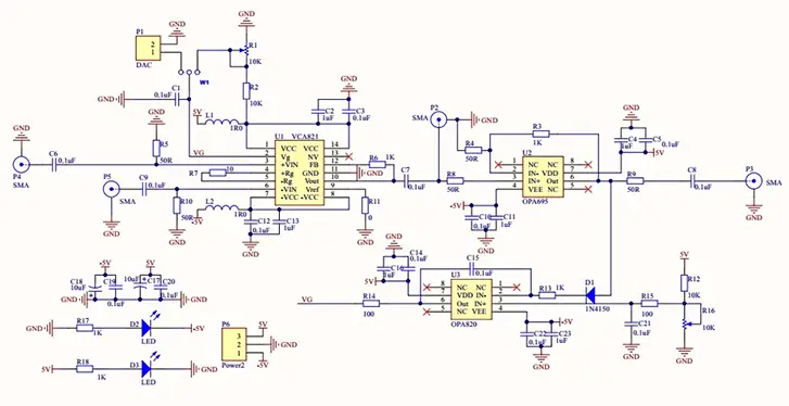
A PCB Schematic Diagram is a blueprint of the electrical connections that form the circuit for a printed circuit board (PCB). This diagram helps us design circuits, visualize the electrical paths between components, and ensure the functionality of the final board before physical production starts. Unlike the physical layout of a PCB, which defines where the components are placed on the board, the schematic diagram primarily focuses on the electrical connections and component relationships.
The schematic diagram is a critical tool that provides clarity during the design process, guides component selection, and forms the foundation for simulating the circuit’s behavior. Additionally, it is essential for error checking and troubleshooting before the actual board is fabricated.
Definition and Purpose of a PCB Schematic Diagram
The PCB schematic diagram serves as the visual representation of the electrical circuit within a PCB design. It shows the interconnection of components such as resistors, capacitors, diodes, transistors, and ICs (Integrated Circuits). Each component is represented by a standard symbol that makes the design easily interpretable. The diagram also includes the power and ground connections to ensure that the electrical pathways are complete and functional.
Understanding the function of PCB Schematic Diagrams: A PCB schematic diagram provides clarity about how electrical current will flow through the board, and it can reveal any potential issues in the circuit before manufacturing begins. It’s like a pre-production test run—ensuring everything is in order and behaves as expected.
How PCB Schematic Diagrams aid in component selection and circuit analysis-
One of the major benefits of a well-crafted schematic is that it acts as a guide for component selection. With accurate schematics, we can easily determine which components are required for the project, whether it’s resistors, capacitors, or more complex devices like integrated circuits. It simplifies the task of sourcing parts, making the process more streamlined and cost-effective.
Moreover, circuit analysis becomes far more efficient when you have a schematic to work with. You can easily identify nodes, voltages, and current flows, and simulate the behavior of the circuit in various scenarios. With this information, we can optimize the design for performance and efficiency.
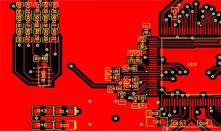
The Relationship Between PCB Schematic Diagrams and the Final PCB Layout
The schematic diagram is directly linked to the PCB layout. Once the schematic is finalized, the next step is translating the schematic into a physical design, where the placement of components and routing of traces take place. The schematic guides the PCB layout designer, ensuring that all components are properly connected and that there is a clear path for signals to flow with minimal interference.
Schematics to PCB Layouts: How To Convert-
●A complete schematic is converted using CAD software to PCB layouts that comprise footprints of the components and ratlines. The term “ratlines” is a bit unpleasant and is used to describe electrical connections that are not yet converted to physical connectors.
●The designer arranges the components and then utilizes the ratlines to guide the design of trace lines, copper pours and vias. The term “via” refers to a tiny through-hole which provides the electrical connections to another PCB surface (or to several layers–e.g. for example, a thermal via might be connected to the ground plane inside the board as well as a ground-connected copper pour at one of the boards’ bottoms).
An accurate schematic is the foundation for a successful PCB layout. Without it, the design might run into roadblocks like signal interference, unexpected short circuits, or uneven power distribution. The schematic acts as your blueprint, ensuring the PCB not only functions as intended but also hits the mark for performance and efficiency. It’s like having a map to avoid detours and dead ends, keeping your project on the right path.
Key Symbols and Components in PCB Schematic Diagrams
To understand a PCB schematic diagram thoroughly, it is essential to recognize the common components and symbols used to represent them. We can rely on a universal set of symbols to communicate complex circuits in a simple and understandable manner. These symbols ensure that everyone involved in the design and manufacturing process is on the same page.
Below is a table showing some common symbols and components typically found in PCB schematic diagrams:
| Component | Symbol | Function |
| Resistor | [Resistor Symbol] | Limits the flow of electric current, used to set voltage levels or control current. |
| Capacitor | [Capacitor Symbol] | Stores electrical energy and smooths out fluctuations in the power supply. |
| Inductor | [Inductor Symbol] | Stores energy in a magnetic field, used for filtering and reducing electrical noise. |
| Transistor | [Transistor Symbol] | A switch or amplifier, critical for controlling the flow of electricity. |
| Integrated Circuit (IC) | [IC Symbol] | A compact collection of components within one package, performing a specific function. |
| Ground | [Ground Symbol] | Provides a common return path for electrical current, acting as the reference point. |
| Power Source | [Power Symbol] | Supplies the required voltage to the circuit, usually marked with Vcc or Vdd. |
These symbols help us identify how the components are linked and provide insight into how the circuit operates. A well-drawn schematic allows everyone involved in the design and manufacturing process to collaborate more effectively, reducing mistakes and saving time.
Benefits of Proper PCB Schematic Diagram Design
The design of a PCB schematic diagram directly impacts the efficiency and success of the entire PCB development process. A well-designed schematic offers a range of benefits, making the design process smoother and more reliable. Let’s break down some of the some advantages.
How a well-designed PCB Schematic Diagram improves manufacturing efficiency-
Crafting a precise schematic diagram sets the stage for a smooth manufacturing process. Acting as a detailed guide to the electrical design, a well-prepared schematic ensures that manufacturers can interpret and implement the design seamlessly. This approach minimizes errors on the production floor, cuts down on wasted time and resources, and keeps rework at bay. For manufacturers focused on delivering top-notch quality, it’s like hitting the sweet spot between efficiency and excellence, all while keeping costs in check.
The Impact of Accurate PCB Schematic Diagrams on Reducing Errors and Rework-
An accurate schematic diagram helps reduce errors during both the design and manufacturing stages. Therefore, we can perform simulations and electrical tests to ensure that the circuit will function as intended. This minimizes the risk of discovering design flaws during the PCB fabrication process, preventing costly rework and delays.
| Benefit | Impact |
| Reduction in Manufacturing Errors | Clear diagrams reduce the likelihood of assembly mistakes and miswiring. |
| Fewer Design Iterations | Engineers can validate the design early on, reducing the need for multiple revisions. |
| Optimized Circuit Behavior | Accurate schematics improve overall circuit performance and reliability. |
Enhancing Design Clarity and Collaboration Through Effective PCB Schematic Diagrams-
A properly designed PCB schematic diagram also promotes better collaboration between different teams. For example, designers, engineers, and manufacturers can all access the schematic to verify their part of the process. This ensures that everyone is on the same page, streamlining the workflow and reducing the chance of miscommunication.
For instance, let’s say there’s a misunderstanding regarding the power connections in a circuit. A clear schematic would highlight the correct paths for power and ground connections, ensuring that the team understands how the power is being supplied to the circuit. In a well-executed schematic, there is no ambiguity—everyone can easily follow the design intent.
The Process of Creating a PCB Schematic Diagram
Designing a PCB schematic diagram follows a step-by-step method that ensures your circuits are both functional and ready for seamless manufacturing. By breaking the process into clear stages, you can address every detail with precision, avoiding common pitfalls and setting yourself up for success. Let’s dive into the workflow to make sure your design ticks all the boxes, from efficiency to reliability, while keeping production hurdles out of the picture.
Step 1: Initial Circuit Design and Component Selection
How to Begin Designing a PCB Schematic Diagram by Selecting Components Based on Project Needs-
The initial circuit design is where the design begins—deciding how your PCB will function. The first task is choosing the right components, which include resistors, capacitors, transistors, and more. You need to ensure that the selected components align with the project specifications, such as voltage, current capacity, and signal types.
Start by defining the overall circuit requirements. Determine the purpose of the circuit, such as power regulation, signal amplification, or signal filtering. Once these parameters are clear, you can select the components that best meet these needs.
The Role of PCB Schematic Diagrams in Optimizing Circuit Performance-
Once the components are selected, the schematic diagram takes over. It allows you to map out the connections between components in a way that ensures optimal circuit performance. By designing with the end goal of performance and efficiency in mind, you avoid unnecessary complexity and power losses. Proper placement of components on the schematic can minimize issues like signal interference and power noise, which can degrade circuit performance.
Cost Considerations When Selecting Components for PCB Schematic Diagrams-
While achieving optimal performance remains a priority, keeping an eye on component costs is just as important during the design process. With prices ranging widely across available options, a thoughtfully crafted PCB schematic diagram helps strike the perfect balance between project requirements and budget constraints. Opting for readily available, off-the-shelf parts or carefully selecting components based on cost-effectiveness and supply can help you save big without skimping on functionality. Smart choices in the design phase often mean fewer headaches—and expenses—down the line.
| Component | Example | Estimated Cost Range |
| Resistor | 1kΩ Resistor | $0.01 – $0.10 |
| Capacitor | 100nF Ceramic | $0.05 – $0.25 |
| Transistor | NPN Transistor | $0.10 – $0.50 |
| IC | LM317 Voltage Regulator | $0.50 – $2.00 |
This table highlights typical price ranges for some commonly used components, offering a sense of how costs can add up based on the components selected.
Step 2: Using CAD Tools for PCB Schematic Diagram Creation
The Importance of CAD Tools Like Altium, Eagle, and KiCad for Creating PCB Schematic Diagrams-
With the components chosen, the next step is moving to Computer-Aided Design (CAD) tools. Tools like Altium Designer, Eagle, and KiCad are specifically built for this task. These tools allow us to draw the schematic, connect components, and perform error checks. CAD tools also come with libraries of standardized components, making it easier to select and place parts on the schematic.
Using CAD tools not only speeds up the design process but also ensures that the schematic is error-free and adheres to industry standards. Most modern CAD tools come with automated checks that flag mistakes such as unconnected pins or incorrect part orientations, preventing costly mistakes before they reach the production stage.
How to Create Accurate and Reliable PCB Schematic Diagrams Using These Tools-
While the tools handle much of the work, it’s up to the designer to use the software effectively. When creating a schematic, please find the follow these steps:
●Place components logically: Group components based on their function (e.g., placing power components in one area, signal components in another).
●Check connectivity: Ensure all components that need to be connected are properly linked with wires.
●Label components clearly: Proper labeling of components, pins, and nets makes it easier for team members and manufacturers to understand the design.
●Use layers effectively: CAD tools allow you to work with multiple layers. Keeping the power, signal, and ground connections separate minimizes confusion and errors.
Benefits of Automated Checks and Validations When Designing PCB Schematic Diagrams-
One of the most valuable features of CAD tools is their ability to automate checks and validations. This drastically reduces human error and speeds up the design process. These tools can check for:
●Floating pins
●Unconnected traces
●Incorrect component values
●Overlapping parts
By catching these mistakes early in the design phase, you can avoid errors that would otherwise cause delays or rework in later stages of production.
Step 3: Signal Routing and Connectivity in PCB Schematic Diagrams
How to Effectively Route Signals in PCB Schematic Diagrams for Optimal Performance-
Once the schematic is drawn, the next important step is signal routing. In this stage, you’ll define how the signal paths are laid out to ensure that the current flow is efficient. Signal integrity is a priority—when designing a PCB schematic, proper signal routing ensures that the circuit operates as intended, without degradation or interference.
The Impact of Layout Design on Signal Integrity and Noise Reduction in PCB Schematic Diagrams-
When it comes to maintaining signal integrity, the schematic layout sets the stage for success. A poorly structured design can introduce headaches like electrical noise or trace cross-talk, disrupting the circuit’s performance. To dodge these pitfalls, it’s essential to nail down proper grounding, strategic decoupling, and smart component placement in the schematic. These design choices keep your circuit humming along smoothly and ensure it stays stable and dependable under real-world conditions.
Best Practices for Ensuring Reliable Signal Flow in PCB Schematic Diagrams-
To ensure reliable signal flow in your PCB schematic diagram, consider the following best practices:
●Minimize trace lengths: Shorter signal paths reduce the chances of interference and signal loss.
●Use proper trace width: Ensure traces are wide enough to handle the current without excessive heating.
●Integrate ground planes: A solid ground plane helps reduce noise and ensures stable operation of signals.
●Separate power and signal traces: Keep power and signal traces apart to avoid interference and cross-talk.
| Best Practice | Explanation | Benefit |
| Minimize trace lengths | Shorter traces reduce interference and signal loss. | Better signal integrity and lower impedance. |
| Use ground planes | A continuous ground plane ensures a stable reference. | Reduces noise and ensures stable operation. |
| Separate power and signals | Keep power traces away from sensitive signals. | Prevents interference and signal degradation. |
Best Practices for PCB Schematic Diagram Design
When designing a PCB schematic diagram, the process requires not only technical precision but also a focus on efficiency and accuracy. By following best practices, we can streamline the workflow, ensure consistency, and meet industry standards that align with global manufacturing requirements. Here’s a breakdown of the practices you should follow when creating a PCB schematic diagram.
Optimizing Workflow for PCB Schematic Diagram Creation
Tips for Streamlining PCB Schematic Diagram Design Processes to Save Time and Reduce Errors-
Designing a PCB schematic diagram can often feel like navigating a maze. However, using some tricks and techniques, you can cut down on design time and reduce the chances of errors. Here’s how you can streamline your workflow:
1.Start with a Clear Plan: Before diving into the CAD software, clearly outline your design objectives and circuit requirements. This includes component specifications, power requirements, and understanding the function of each component in the circuit.
2.Use Predefined Templates: Most PCB design software comes with templates that allow for quick setup and ensure consistency across projects. These templates include standard component libraries, trace widths, and voltage ratings, making it easier to begin the design process without having to set everything from scratch.
3.Leverage Auto-Routing Tools: Modern CAD tools offer auto-routing features that help automatically create connections between components. While you should review these automated routes, they can save time and reduce the manual effort required, especially for complex designs.
Utilizing Standard Libraries and Templates for PCB Schematic Diagrams-
Using standardized component libraries in PCB schematic design simplifies the entire process and boosts reliability. These libraries provide pre-verified symbols and footprints for common components like resistors, capacitors, transistors, and ICs, making it easier to maintain accuracy and consistency throughout your project. By sticking to industry-approved conventions, you reduce the chances of errors sneaking into your design and ensure smooth compatibility with global manufacturing processes. Think of it as cutting through the red tape while keeping everything on the up and up.
Additionally, templates can help you quickly establish your design structure, from basic component placements to wire routing. Standardized templates make it easier to ensure the circuit design is consistent across multiple projects, which can be a significant time-saver.
Ensuring Team Collaboration Through Version Control in PCB Schematic Diagrams-
Collaboration is key, especially in large engineering teams. Version control systems like Git or built-in features in CAD software can help ensure everyone on the team works from the latest schematic version. By tracking changes, you can avoid design conflicts, ensure that all team members are on the same page, and ensure traceability of modifications.
| Best Practice | Explanation | Benefit |
| Clear Planning | Outline your project before starting the schematic. | Reduces design time and minimizes mistakes. |
| Predefined Templates | Use libraries and templates for standard components and layouts. | Streamlines the design process and ensures consistency. |
| Version Control | Implement version control software like Git for collaboration. | Keeps track of changes and prevents errors caused by conflicting updates. |
Maintaining Consistency and Accuracy in PCB Schematic Diagrams
Importance of Consistent Component Footprints and Symbols in PCB Schematic Diagrams-
When designing a PCB schematic diagram, consistency is absolutely non-negotiable.. Every component used in the schematic must adhere to standardized footprints and symbols. By using standardized component libraries, you ensure that every part has the correct shape, pin configuration, and electrical properties. Consistency in footprints guarantees that the components fit in the final PCB layout, which helps avoid misalignments during manufacturing and assembly.
Consistency also extends to labeling components in the schematic. Each part should be clearly labeled with its value (e.g., 1kΩ resistor), part number, and a description. By adhering to these standards, you create a schematic that is easier to understand, review, and manufacture.
How to Maintain Accuracy During Schematic Design Reviews and Validations-
Design reviews and validation checks are a must when it comes to ensuring your PCB schematic is on point. During the review process, you and your team will go through the schematic to confirm that it ticks all the boxes—component selection, signal routing, and power connections all need to line up with the design specs. Think of it like a final check before hitting the green light—this step helps catch any missteps early, saving you time and money down the line. It’s all about making sure everything aligns perfectly before you move forward with the next phase.
1.Cross-Check for Errors: Always verify that all components are correctly placed and labeled. Check for floating pins or unconnected signals that could lead to malfunctions in the final product.
2.Use Validation Tools: Most PCB design tools offer automated validation checks, such as verifying the electrical properties of connections. These tools will scan for issues like incorrect connections, unconnected nets, and incompatible components.
3.Peer Review: Collaborate with colleagues or external engineers to review your schematic design before finalizing it. A fresh set of eyes can catch issues you might have overlooked.
Ensuring Correct Electrical Connections in PCB Schematic Diagrams-
One of the most common errors in PCB design is incorrect electrical connections between components. When working on a schematic diagram, it’s important to:
●Label all connections: Proper labeling ensures that each connection between components is clear.
●Double-check pin configurations: Ensure that pins and connections align with the components’ specifications, especially for ICs.
●Validate signal flow: Check that signals are flowing in the right direction and that power rails are correctly distributed.
Adhering to Industry Standards for PCB Schematic Diagrams
Overview of IPC Standards for PCB Schematic Diagrams and How to Comply with Them-
The IPC standards, set by the Institute for Printed Circuits, are recognized globally as the benchmarks for PCB design, including schematic diagrams. These standards define everything from component placement to connection rules, ensuring quality and interoperability between designs.
IPC standards ensure that:
●Components are placed correctly for manufacturing processes.
●Schematic diagrams are understandable by engineers, fabricators, and testers.
●The design adheres to global standards for electrical and mechanical performance.
For example, following IPC-2221 ensures that your design will meet electrical integrity requirements for high-frequency circuits.
How PCB Schematic Diagrams Impact Regulatory Approvals for Consumer Electronics-
When designing PCBs for consumer electronics, regulatory approvals are often required before the product can be mass-produced. These approvals typically come from organizations like FCC, CE, or UL. A well-designed PCB schematic diagram that complies with industry standards greatly enhances the likelihood of regulatory approval.
For example, FCC compliance for electronic devices often requires that the schematic avoids introducing electromagnetic interference (EMI). Proper grounding, power decoupling, and shielding can be integrated directly into the schematic to ensure regulatory compliance.
Advanced Concepts in PCB Schematic Diagrams
Creating effective PCB schematic diagrams isn’t just about placing components and connecting them — it’s about understanding the complexities that go into high-performance designs. As technology advances, PCB schematic diagrams must handle increasingly complex requirements, especially in fields like signal integrity, high-speed circuits, and manufacturability. Below, we dive into advanced concepts that can take your PCB schematic diagrams to the next level.
Signal Integrity in PCB Schematic Diagrams
Signal integrity is a factor to consider when designing PCB schematic diagrams, especially in high-performance circuits. Poor signal handling can lead to issues like signal degradation, noise, or interference, all of which can mess with your circuit’s functionality. A well-designed schematic helps ensure that all components and connections are mapped out correctly, which supports smooth signal flow. By addressing potential issues at the schematic level, you can avoid problems that might arise later in the design process, ensuring your system operates as expected. It’s all about keeping things clear and precise from the start to prevent hiccups down the road.
The Role of PCB Schematic Diagrams in Maintaining High Signal Integrity for Complex Circuits-
In complex designs, PCB schematic diagrams act as the first line of defense against signal integrity issues. Proper component placement and routing in the schematic can prevent issues such as cross-talk, reflection, and signal loss. For instance, ensuring proper grounding and decoupling techniques in the schematic helps reduce noise and power fluctuations, which can affect signal clarity.
Schematic designs also influence the physical PCB layout. A well-designed schematic ensures that signal paths are minimized and properly routed, reducing interference and ensuring that signals travel without unwanted distortion. For complex, high-speed circuits, understanding how signal paths interact can prevent long-term issues in the manufacturing stage.
Techniques to Minimize Signal Degradation and Noise in PCB Schematic Diagrams-
Signal degradation and noise can be reduced by following several techniques when creating the PCB schematic diagram:
1.Use of Differential Pairs: Differential signals, often used in high-speed circuits, should be routed as pairs to maintain the integrity of the signals. Schematic design should ensure that these pairs are tightly coupled to minimize external noise.
2.Ground Planes and Decoupling Capacitors: Proper grounding in the schematic helps to create stable reference points for signals, while decoupling capacitors minimize power supply noise and prevent signal degradation.
3.Minimizing Loop Areas: Keeping loops as small as possible in the schematic ensures that any potential noise does not have room to affect the signal paths.
4.Impedance Matching: Impedance mismatches between signal traces and components can lead to signal reflections and loss. The schematic design should consider the required impedance of traces and ensure that the components used match those specifications.
| Signal Integrity Techniques | Explanation | Benefit |
| Use of Differential Pairs | Routing signals in pairs to reduce noise interference. | Enhances signal clarity and reduces noise. |
| Grounding and Decoupling | Proper grounding and use of decoupling capacitors. | Reduces power fluctuations and maintains stable signals. |
| Minimizing Loop Areas | Reducing the physical area where current flows in the schematic. | Prevents electromagnetic interference and signal degradation. |
Understanding the Effects of Parasitics in PCB Schematic Diagrams-
Parasitic components, such as capacitance, inductance, and resistance, can significantly impact the performance of a circuit. These parasitics are inherent in all physical PCB designs, and their effects are often first visible in the schematic phase. Designing with parasitics in mind can help avoid performance degradation.
By simulating the schematic with parasitic effects incorporated, we can anticipate potential issues and mitigate them before they become problems in the PCB layout.
PCB Schematic Diagrams for High-Speed Circuits
Designing PCB schematic diagrams for high-speed circuits requires special consideration due to the rapid transmission of signals and the sensitivity of the components involved. High-speed circuits, especially those used in RF applications or digital systems, need precise and careful design to ensure signal integrity and prevent failures.
Unique Challenges of Designing PCB Schematic Diagrams for High-Frequency Applications-
High-frequency applications present several challenges when creating PCB schematic diagrams. One of the biggest concerns is the signal degradation caused by parasitic inductance and capacitance. These can cause delay, reflection, and loss of signal quality, especially at frequencies above several gigahertz.
The schematic must carefully account for these effects by selecting appropriate components, considering trace lengths, and ensuring the design minimizes any path that could create impedance mismatches.
How to Ensure Signal Integrity in PCB Schematic Diagrams for High-Speed Digital and RF Circuits-
Ensuring signal integrity in high-speed designs requires several strategies:
1.Proper Termination: In high-speed circuits, terminating the signal traces appropriately is necessary to avoid reflections. The schematic should include the correct termination resistors to match the impedance of the traces.
2.Controlled Impedance Routing: For high-speed circuits, it is essential to route traces with a controlled impedance. The schematic design should specify the required impedance values to prevent signal reflection and degradation.
3.Minimizing Trace Lengths: Longer signal paths in the schematic increase the risk of noise, interference, and signal degradation. Shorter traces minimize these risks and help maintain signal integrity.
4.Separation of Power and Signal Lines: Separating power and signal lines in the schematic helps prevent cross-talk and reduces the likelihood of power noise interfering with the signal.
Managing Impedance and Trace Length in High-Speed PCB Schematic Diagrams-
In high-speed designs, it’s all about managing impedance and trace lengths to make sure your signals travel cleanly without distortion. Things like trace width, layer stack-up, and the spacing between traces need to be dialed in perfectly. If not, you risk signal integrity issues that could throw off the whole circuit. A well-planned design ensures that impedance is kept in check, preventing unwanted noise or loss of signal quality. It’s like making sure the roads are smooth and clear for your signals to take the fast lane without any bumps or detours.
Using simulation tools early in the schematic design process helps predict how the traces will behave and allows us to tweak the design before physical manufacturing. Incorporating these factors into the PCB schematic diagram ensures a reliable, high-performance circuit in the final product.
Design for Manufacturability in PCB Schematic Diagrams
Designing PCB schematic diagrams with manufacturability in mind is necessary to ensure the final product is cost-effective, easy to produce, and error-free. This process involves selecting components, layouts, and designs that align with the manufacturer’s capabilities to minimize production delays.
How to Design PCB Schematic Diagrams that Align with Manufacturing Capabilities-
When creating PCB schematic diagrams, it’s important to consider the limitations and capabilities of your manufacturing process. Some design features that may be viable on paper may not be feasible for mass production due to cost, manufacturing limitations, or material constraints.
Ensure that the schematic reflects components and layouts that are available and manufacturable at scale. For example, specifying commonly available components in the schematic reduces the risk of sourcing delays or supply chain issues.
Cost-Saving Strategies in PCB Schematic Diagrams through Material Selection and Efficient Layout-
Cost savings can be achieved through material selection and optimizing the layout. The schematic can specify components that balance cost with performance. Choosing components with better availability or lower cost can drastically reduce production costs without compromising the quality of the design.
Additionally, careful layout planning in the schematic phase can optimize the use of space and reduce the number of layers in the PCB, thus lowering the overall manufacturing cost.
Reducing Production Delays with Accurate PCB Schematic Diagrams-
An accurate PCB schematic diagram reduces production delays by minimizing the likelihood of errors during the manufacturing process. An inaccurate schematic can lead to problems during the board layout, assembly, or even testing stages, which can cause significant delays and additional costs.
By thoroughly reviewing the schematic and ensuring its accuracy, you can avoid these delays and keep the production process on track.
Troubleshooting and Validation of PCB Schematic Diagrams
The creation of PCB schematic diagrams is a detailed and iterative process. Even experienced engineers encounter challenges that can compromise the quality and performance of a final design. Ensuring that PCB schematic diagrams are error-free and properly validated is a critical part of the design process. Let’s explore how to identify common errors, effectively troubleshoot issues, and validate PCB schematic diagrams to ensure reliable and functional designs.
Common Errors in PCB Schematic Diagrams and How to Avoid Them
PCB schematic design is not just about arranging components and wiring them together; it’s about ensuring the design functions as intended when translated into a physical PCB. There are several common errors that can arise during schematic design. By understanding these potential pitfalls, we can create more reliable designs.
Identifying Common Mistakes in PCB Schematic Diagrams-
1.Missing Components: One of the most frequent issues that can arise is forgetting to include necessary components in the schematic. These components could be passive elements like resistors or capacitors, or active components like ICs or voltage regulators. Missing components can lead to incomplete circuits, causing system failures after assembly.
2.Incorrect Connections: Another common mistake is improper connections between components. A simple wire crossing or misconnected pin can disrupt signal flow or cause a short circuit. These errors are often difficult to catch manually, which is why automated checks become invaluable.
3.Overlapping Wires and Nets: While designing the schematic, our engineers might accidentally overlap wires, causing unintentional connections or short circuits. These problems can be hard to notice in complex designs, but their consequences are far-reaching.
Best Practices for Error-Free PCB Schematic Diagrams Creation-
To reduce the likelihood of errors, the following best practices can be implemented:
●Component Checklists: Always create a component checklist before beginning the schematic design. This ensures that every necessary part is included and correctly placed.
●Connection Verification: Regularly verify connections, especially for core components like ground, power, and signal paths. Running consistency checks ensures that no components are left floating or connected incorrectly.
●Reviewing and Cross-Referencing: Regularly review the schematic against the design specifications and cross-reference it with simulation results to ensure everything is in place and functioning as intended.
Using Validation Tools to Check for Unconnected Nets and Overlap Issues in PCB Schematic Diagrams-
Most modern PCB design tools offer built-in validation features that can help detect errors in the schematic. Tools like Altium Designer, KiCad, and Eagle automatically flag common issues such as:
●Unconnected Nets: These are signals or power paths that have not been properly connected to their respective components. If left unconnected, the circuit will fail to work.
●Overlap Issues: Overlapping wires or components that cause physical or electrical conflicts. These errors often go unnoticed in a manual review.
These tools offer automated error checking that allows us to identify and address these problems early in the design process, reducing the risk of costly revisions later.
| Common Errors | Description | Solution |
| Missing Components | Omitting essential components like capacitors or resistors. | Use a component checklist and validate part selection. |
| Incorrect Connections | Miswiring components or missing connections. | Regularly verify schematic against design specifications. |
| Overlapping Wires/Nets | Unintentional wire overlaps or shorts. | Use validation tools for overlap detection. |
Testing and Debugging PCB Schematic Diagrams
Before moving on to PCB layout and physical prototyping, taking the time to debug your PCB schematic diagrams is a no-brainer. This step helps uncover design missteps and ensures the schematic functions as intended, saving you from headaches and pricey hiccups during the manufacturing phase. Catching issues early not only smooths out the design-to-production process but also keeps your project on the fast track to success.
Techniques for Debugging Issues in PCB Schematic Diagrams Before Moving to Layout-
●Schematic Simulation: One of the most powerful debugging techniques is simulation. Modern PCB design software allows you to run simulations of your schematic to check for functional correctness. You can simulate voltage, current, and signal flow through the schematic to ensure there are no errors before moving on to layout.
●Trace Analysis: During schematic debugging, always check the trace paths for signal quality, especially in high-speed designs. Identify potential issues like excessive trace length or improper component placement that may cause signal degradation.
Using Simulation Tools to Verify Functionality and Signal Integrity in PCB Schematic Diagrams-
Simulation tools like SPICE, HyperLynx, or integrated simulators in tools like Altium can provide valuable insights. You can simulate the following aspects:
●Signal Integrity: Verify that the signals maintain their quality and do not distort or lose power during transmission.
●Power Integrity: Ensure that all power paths are capable of delivering the necessary current without excessive voltage drop.
●Timing Analysis: In high-speed designs, perform timing analysis to check for timing errors like race conditions or setup/hold violations.
Troubleshooting Manufacturing Issues by Reviewing the PCB Schematic Diagram-
When issues arise during PCB manufacturing or assembly, the first place to start troubleshooting is often the schematic. Reviewing the schematic allows you to pinpoint areas where the design might not align with manufacturing capabilities or where human error may have occurred during assembly. Common problems include:
●Component Placement Errors: If the physical component placement doesn’t align with the schematic, it can result in incorrect connections.
●Missing or Incorrect Labels: If the schematic lacks proper labeling for test points, power rails, or component values, it can cause confusion on the assembly line.
●Design Rule Violations: A quick review of the schematic can help identify if any design rules related to component placement or spacing were violated.
A comprehensive schematic review during manufacturing can save time, reduce rework, and avoid production delays.
| Testing/Debugging Method | Purpose | Tools |
| Schematic Simulation | Verify functionality and performance of the circuit. | SPICE, HyperLynx, Altium Designer Simulation |
| Signal Integrity Testing | Ensure signal integrity through the schematic. | Signal integrity simulation tools in CAD software |
| Power Integrity Analysis | Verify the reliability of power delivery across the circuit. | Power analysis tools in CAD software |
| Manufacturing Review | Check for alignment with manufacturing capabilities. | Design rule checks in CAD tools, thorough schematic review |
Advanced Tools and Techniques for PCB Schematic Diagram Design
In today’s rapidly advancing design landscape, PCB schematic diagrams ensure electronic systems are dependable, high-performing, and tailored for efficiency. Achieving excellence in this process calls for adopting sophisticated design tools, leveraging automated error detection, and integrating external libraries effectively. By making informed choices about CAD software, utilizing built-in verification features, and incorporating third-party resources, we can craft schematics that are accurate, streamlined, and production-ready. Let’s explore the strategies and techniques that elevate schematic design while keeping the workflow smooth as butter.
Choosing the Right CAD Tools for PCB Schematic Diagrams
The choice of CAD tools directly influences the effectiveness and efficiency of the PCB design process. With numerous software packages available, it is important to consider a toolset that meets both your current design requirements and potential future needs.
A Comparison of Popular CAD Tools Used in PCB Schematic Diagram Creation-
Several CAD tools are commonly used in PCB schematic diagram creation, each with its own set of strengths. Here’s a brief comparison of some of the most popular options:
| CAD Tool | Key Features | Best For |
| Altium Designer | High-level integration for PCB design, real-time collaboration, advanced simulation features. | Complex designs requiring collaboration and high-speed routing. |
| Eagle | User-friendly interface, extensive component library, strong community support. | Hobbyists and small-scale designs. |
| KiCad | Open-source, versatile with extensive component libraries and powerful routing tools. | Cost-effective for startups and educational purposes. |
| Autodesk Fusion 360 | Cloud-based tool with mechanical, electrical, and PCB design integration. | Integrated design workflows across disciplines. |
Features of Advanced CAD Tools That Improve the Design and Simulation of PCB Schematic Diagrams-
Advanced CAD tools for PCB schematic diagrams offer features that streamline the design process, reduce errors, and increase efficiency. These include:
●Real-time Simulation: Many tools now integrate real-time circuit simulation, allowing us to validate our schematics before moving on to the layout stage.
●Signal Integrity Analysis: Tools like Altium Designer and Cadence Allegro come equipped with signal integrity analysis, helping engineers visualize and troubleshoot issues like cross-talk and signal degradation.
●Multi-Layer Design: For complex PCBs, CAD tools offer multi-layer design capabilities to accommodate dense circuits and multiple signal paths without compromising performance.
How to Integrate Third-Party Libraries and Tools with Your PCB Schematic Diagram-
Third-party libraries and additional tools enhance a PCB schematic diagram’s flexibility and functionality. We can integrate external component libraries, simulation tools, and DRC (Design Rule Check) add-ons with their primary CAD software. Popular integrations include:
●Component Libraries: Importing standard or custom component libraries from suppliers like DigiKey, Mouser, or SnapEDA allows for streamlined part selection and quick design validation.
●Simulation Tools: Integrating external simulators like SPICE for analog and mixed-signal analysis helps verify circuit behavior under various conditions.
Automated Design Checks in PCB Schematic Diagrams
Automation plays an integral role in modern PCB schematic diagram creation. It is not just about designing a circuit; it’s about ensuring that the design is functional, manufacturable, and free from errors. Automated design checks provide a safety net, ensuring that every connection is valid, all components are correctly placed, and no design rules are violated.
The Benefits of Automated Rule Checking in PCB Schematic Diagrams-
Automated rule checking is a critical component of the PCB schematic diagram process. It helps:
●Reduce Human Errors: Manual checks can easily overlook small but critical mistakes, such as incorrect component values, missing connections, or misplaced traces. Automated checks flag these errors before they progress further into the design process.
●Ensure Compliance with Design Rules: Tools can automatically ensure that designs adhere to electrical, mechanical, and manufacturing design rules, reducing the risk of issues during the PCB manufacturing phase.
How to Integrate Automated Checks for Electrical Integrity and Design Errors in PCB Schematic Diagrams-
To maintain a high standard of design integrity, automated checks can be applied across several stages of the PCB schematic diagram creation:
●Electrical Integrity Checks: Software tools such as Altium Designer and KiCad integrate electrical rule checks (ERC) that detect common issues like unconnected nets, incorrect net assignments, and floating pins.
●Design Rule Checks (DRC): These checks ensure that the schematic conforms to set guidelines related to trace width, spacing, and component alignment. DRCs also check for errors like shorts, overlapping connections, and missing power or ground paths.
Ensuring Consistency and Quality with Automated Validations in PCB Schematic Diagrams-
Automated validation tools work in conjunction with ERC and DRC to check for:
●Consistency: Ensuring that all component footprints and pin configurations match between the schematic and the final layout.
●Design Quality: Verifying that the schematic is clean and organized, with components correctly placed for future assembly and testing.
By automating these validation processes, designers can maintain a consistent, high-quality schematic design that is ready for the next phase of PCB development. This process also reduces the likelihood of design iterations due to overlooked errors.
| Automated Check | Purpose | Tool Integration |
| Electrical Rule Check (ERC) | Detect electrical errors such as unconnected nets and shorts. | Altium Designer, Eagle, KiCad |
| Design Rule Check (DRC) | Ensure adherence to physical and electrical design rules. | Altium Designer, Eagle, KiCad |
| Component Validation | Verify correct component placement and footprint matching. | KiCad, Altium Designer |
How PCB schematic diagrams drive efficiency in PCB Manufacturing?
Integrating BOM with PCB Schematic Diagrams
The Bill of Materials (BOM) is another essential component of PCB schematic diagram design, directly linked to the overall manufacturing process. When properly integrated, the BOM and schematic diagrams can eliminate manual errors, improve inventory management, and ensure that the right parts are available at the right time. Here’s how to make this integration work effectively:
Streamlining BOM Integration-
A well-detailed BOM should be an output from the schematic design process, linking each component in the diagram to its respective part number, value, and manufacturer. This integration allows:
●Automated Part Ordering: Once the schematic diagram is completed, the BOM can be used for ordering parts directly, avoiding delays caused by incorrect part numbers or missing components.
●Inventory Management: By ensuring that all components in the BOM match the schematic, we can track part usage more effectively, reducing the chances of excess inventory or stockouts.
Aligning BOM with PCB Design Specifications-
Integration also requires ensuring that the BOM accounts for all design details, including:
●Component Values and Ratings: Ensuring that the values listed in the BOM align with the schematic’s component specifications, reducing the risk of ordering incorrect parts.
●Packaging Details: For parts that require specific packaging formats for automated placement machines, including this in the BOM ensures smoother assembly.
| BOM Integration | Benefit | Impact |
| Automated Part Ordering | Minimizes errors and delays in the supply chain | More efficient part procurement and assembly |
| Inventory Management | Prevents overstocking or stockouts | Improved cost control and less waste |
| Detailed Component Specifications | Ensures the right components are sourced and used | Increased design reliability and accuracy |
This integration isn’t just about data accuracy; it’s a direct contributor to faster, more accurate production cycles, ensuring that manufacturing teams have everything they need, exactly when they need it.
Minimizing Manufacturing Errors with Accurate PCB Schematic Diagrams
Manufacturing errors can be a significant cost driver in high-volume production environments, leading to delays, rework, and scrapped PCBs. Ensuring that PCB schematic diagrams are precise, well-organized, and fully validated can drastically reduce these errors.
Best Practices for Error-Free Schematic Diagrams-
The best way to minimize manufacturing errors is to ensure the schematic diagram is clear, complete, and thoroughly checked before proceeding to the layout stage. Key practices include:
●Component Verification: Ensure that each component is correctly defined, with its specifications matching the schematic requirements, including orientation and footprint.
●Signal Path Verification: Double-check that all signal paths are correctly routed and that there are no conflicts with power/ground planes.
Utilizing Validation Tools-
With modern CAD tools, automated validation can catch errors early in the design process. Tools that check for:
●Unconnected Nets: These errors can often go unnoticed in manual reviews but are easily detected by automated checks.
●Overlapping Connections: Ensuring that no two components have their pins or leads accidentally connected reduces the chance of faulty designs.
| Validation Tool | Purpose | Benefits |
| ERC (Electrical Rule Check) | Detects unconnected nets and invalid connections | Reduces errors early in the design process |
| DRC (Design Rule Check) | Verifies that all components comply with design constraints | Ensures manufacturability and prevents costly production errors |
| Signal Integrity Check | Checks for potential signal degradation or interference | Enhances overall product reliability |
By utilizing these validation techniques and ensuring that the PCB schematic diagram is both complete and correct, we can significantly reduce the number of costly errors that would otherwise arise in the production phase.
FAQ&PCB Schematic Diagram
Why is a PCB Schematic Diagram necessary for PCB design?
It helps designers visualize the circuit before creating the physical PCB, ensuring proper component placement and connections.
What are the key components in a PCB Schematic Diagram?
Common components include resistors, capacitors, transistors, ICs, and connectors, each represented by specific symbols.
What CAD tools are commonly used for PCB Schematic Diagram creation?
Popular tools include Altium Designer, Eagle, KiCad, and OrCAD, offering features like schematic capture and simulation.
How do PCB Schematic Diagrams affect manufacturing?
Accurate schematics ensure proper component placement, minimizing errors and production delays during the manufacturing process.
What is the role of a Bill of Materials (BOM) in PCB Schematic Diagrams?
The BOM lists all components used in the design, providing essential information for procurement, assembly, and testing.
How can signal integrity be maintained in PCB Schematic Diagrams?
Proper routing, minimizing noise, and using correct trace widths and lengths help maintain signal integrity in high-frequency circuits.
What are common mistakes in PCB Schematic Diagrams and how can they be avoided?
Missing components, incorrect connections, and inconsistent symbols are common errors. Using validation tools and following best practices can prevent these issues.


