
Introduction:
Nelco N4000-29 is a high-performance laminate selected for advanced circuit boards destined for demanding high-speed and high-frequency operation. Realizing the full capabilities of this material is contingent upon a profound understanding of specialized design disciplines, precision fabrication techniques, and meticulous assembly protocols. This guide provides comprehensive information for advanced engineering projects, serving as a definitive technical resource. Its purpose is to inform design choices and illuminate how expert fabrication transforms complex schematics into dependable, high-performance hardware.
What is Nelco N4000-29?
The Nelco N4000-29 laminate system is specified for multilayer printed circuit boards (PCBs) that must function reliably under challenging electrical and thermal conditions. It is built on a high-performance, multifunctional epoxy resin, delivering a superior balance of signal integrity, thermal stability, and manufacturability when compared to standard FR-4 materials.
Material Composition and Structure
The foundation of Nelco N4000-29’s performance lies in its constituent elements.
● Resin System: It utilizes an advanced multifunctional epoxy resin matrix, providing a high crosslink density. This composition is the source of its exceptional thermal and chemical resistance.
● Reinforcement: It employs a standard E-glass woven fabric for reinforcement, offering excellent mechanical strength, dimensional stability, and a favorable cost structure.
● Copper Foil: The system is compatible with a wide range of copper foils, including standard electro-deposited (ED), reverse-treated (RT), and various low-profile (LP) options to suit different performance needs.
Primary Application Space
This material is engineered to occupy the space between conventional FR-4 and more exotic, high-cost RF/microwave laminates.
● High-Speed Digital: Suited for systems with fast signal rise times and high data rates, such as network routers, servers, data storage, and automated test equipment (ATE).
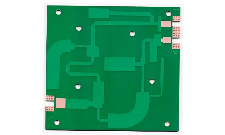
● High-Frequency RF: Applicable for many RF designs operating up to the ~15-20 GHz range, including telecommunications infrastructure, amplifiers, and filters where stable electrical properties are required.
Core Electrical and Mechanical Specifications
A material’s performance is defined by its data sheet values. A comprehension of these specifications is the first step in successful engineering. Below are the foundational properties of Nelco N4000-29.
Electrical Properties
These parameters govern how electrical signals behave as they propagate through the material.
| Property | Value |
| Dielectric Constant (Dk) | 3.7 @ 10 GHz |
| Dissipation Factor (Df) | 0.008 @ 10 GHz |
| Volume Resistivity | High |
| CAF Resistance | High |
● Dielectric Constant (Dk): Nominally 3.7 at 10 GHz. This stable, low Dk facilitates faster signal propagation and predictable impedance control.
● Dissipation Factor (Df): Nominally 0.008 at 10 GHz. This low loss tangent minimizes signal energy absorption, preserving signal amplitude (insertion loss) over long distances and at high frequencies.
● Volume Resistivity: High electrical insulation properties ensure minimal current leakage between conductive layers.
● CAF Resistance: The material exhibits high resistance to Conductive Anodic Filament (CAF) formation, a reliability factor for high-density designs in humid environments.
Thermo-Mechanical Properties
These parameters define the material’s physical robustness during manufacturing and its operational life.
| Property | Value |
| Glass Transition Temp (Tg) | >210°C |
| Decomposition Temp (Td) | >380°C |
| CTE (Z-axis) | Low, matched to copper |
| Flexural Strength | High |
● Glass Transition Temperature (Tg): Greater than 210°C. A high Tg ensures the material remains rigid and stable during high-temperature lead-free assembly, preventing warpage.
● Decomposition Temperature (Td): Greater than 380°C. This provides a wide safety margin above soldering temperatures, preventing irreversible chemical degradation of the resin.
● Coefficient of Thermal Expansion (CTE): The material features a low Z-axis CTE, closely matched to copper. This attribute minimizes stress on plated through-holes (vias) during thermal cycling, greatly enhancing long-term reliability.
● Flexural Strength: High mechanical strength ensures the board can withstand the physical stresses of assembly and handling without fracturing.
Signal Integrity by Design: Layout Guidelines for N4000-29
The preservation of signal integrity (SI) is a fundamental objective in high-speed design. Layout choices directly dictate performance. Adherence to established SI principles when designing with Nelco N4000-29 is a prerequisite for success.
Controlled Impedance Routing
Traces at high frequencies behave as transmission lines, and their impedance must be managed.
| Aspect | Best Practice | Purpose |
| Microstrip/Stripline | Use precise trace width and dielectric height for impedance targets | Achieve 50Ω (single-ended), 100Ω (differential) routing |
| Reference Planes | Route signals over continuous ground or power planes | Ensure return path integrity and minimize EMI |
| Geometry Consistency | Maintain uniform width/spacing throughout trace length | Avoid impedance discontinuities and reflections |
●Microstrip and Stripline: Utilization of proper geometries (trace width, dielectric height) for outer-layer microstrip and inner-layer stripline traces allows for achieving target impedances (e.g., 50Ω single-ended, 100Ω differential).
●Reference Planes: High-speed signals should be routed over a solid, continuous reference (ground or power) plane to provide a clear return path and minimize noise. Routing over splits in the reference plane should be avoided.
●Consistent Geometries: A uniform trace width and spacing must be maintained for the entire length of a controlled-impedance line to avoid reflections.
Crosstalk Mitigation
Crosstalk is the unwanted electromagnetic coupling of signals between adjacent traces.
| Technique | Description | Effectiveness |
| Trace Spacing | Space traces ≥3x trace width (3W rule) | Reduces near-end and far-end crosstalk |
| Orthogonal Routing | Alternate routing directions on adjacent layers | Reduces broadside coupling between layers |
| Guard Traces | Grounded trace with stitching vias between sensitive signals | Provides additional electromagnetic shielding |
●Trace Spacing: Increasing the spacing between parallel high-speed traces is a primary mitigation technique. A general guideline is to maintain a space at least 3x the trace width (3W rule).
●Orthogonal Routing: Routing signal layers in alternating directions (e.g., Layer 3 horizontal, Layer 5 vertical) minimizes broadside coupling between layers.
●Guard Traces: For highly sensitive signals, routing a grounded guard trace parallel to the signal trace, with stitching vias along its length, provides additional isolation.
Via and Layer Transition Design
Vias are a major source of impedance discontinuities if not properly designed.
●Stub Minimization: The unused portion of a via barrel (the “stub”) can cause resonant reflections. For very high-speed signals (>10 Gbps), specifying back-drilling to remove these stubs is a common practice.
●Return Path Vias: Placing ground vias in close proximity to signal vias during layer transitions provides a continuous return path for the signal. This prevents large, noisy current loops.
●Pad and Annular Ring: A sufficient annular ring (the copper pad area around a drilled hole) ensures a reliable connection after drilling and plating operations.
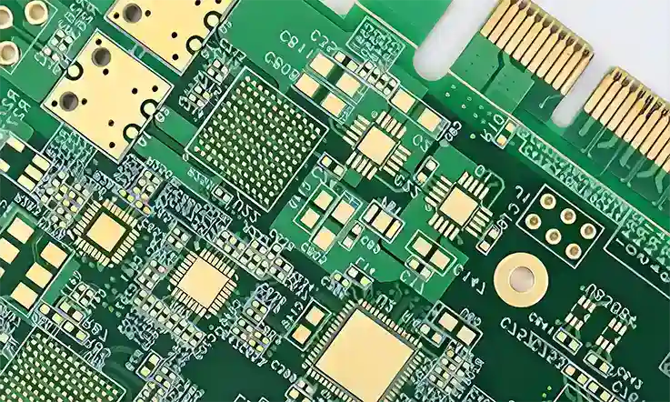
High-Speed Digital Design: Advanced Considerations
As data rates escalate beyond 28 Gbps into the 56 Gbps and 112 Gbps PAM4 signaling space, second-order electrical effects that were once negligible become dominant sources of channel degradation. Designing with Nelco N4000-29 for these leading-edge applications requires a deeper level of analysis and specific mitigation techniques.
Managing Skew and Jitter
At high data rates, timing precision is absolute.
●Intra-Pair Skew: This timing difference between the two lines of a differential pair must be minimized. This is accomplished by ensuring the physical lengths of the P and N traces are meticulously matched, often to within 1-2 mils.
●Channel-to-Channel Skew: In parallel data buses, the timing difference between different channels also requires control through careful length matching across the entire bus.
●Jitter Budget: Jitter (timing uncertainty) is induced by various factors, including material properties, reflections, and crosstalk. An effective design minimizes these factors to stay within the channel’s overall jitter budget, which is a condition for achieving a low Bit Error Rate (BER).
The Fiber Weave Effect and Mitigation
At frequencies above 10 GHz, the reinforcement pattern of the glass fabric within the laminate can affect signal propagation.
●Mechanism: The woven glass reinforcement creates periodic variations in the local Dk value, depending on whether a trace runs over a resin-rich area (knuckle) or a glass-rich area (opening). This can lead to unpredictable skew and impedance variations.
●Mitigation Strategies: Several strategies can combat this effect. One is to route critical traces at a slight angle (e.g., 5-10 degrees) relative to the glass weave axis. Another is to specify laminates with flatter glass styles (like 1078 or 1086 glass), with which Nelco N4000-29 can be procured for sensitive applications. Advanced simulation tools can also model and account for this effect.
Insertion Loss Budgets and S-Parameter Analysis
Every element in a high-speed channel contributes to signal loss.
●Loss Budget: A total insertion loss budget is allocated for the entire channel, and the PCB’s contribution must be carefully managed. The low Df of N4000-29 provides a distinct advantage in this regard.
●S-Parameter Models: For sensitive channels, pre-layout simulation using S-parameter (Scattering parameter) models is strongly advocated. Accurate material characterization data can be used to feed these models, allowing designers to predict channel performance, including insertion loss (Sdd21) and reflections (Sdd11), before committing to fabrication.
The Function of Back-Drilling in SERDES Channels
For SERDES (Serializer/Deserializer) channels at 28 Gbps and above, back-drilling is a frequently specified process.
●Stub Resonance: A via stub can behave as a resonant antenna. At a frequency where the stub is a quarter wavelength, it creates a deep null in the frequency response, which can severely close the signal’s eye diagram.
●Stub Removal: Back-drilling is a controlled-depth drilling process that mechanically removes the unused via stub after the main through-hole has been plated. This action eliminates the resonant null and improves signal integrity.
●Design and Fabrication: The process requires careful design specification and precise fabrication control to ensure the correct depth is achieved without damaging the active portion of the via.
Navigating the complexities of high-speed channel design? Request a consultation to discuss your signal integrity requirements.
DFM Guidelines: Ensuring Manufacturability and Yield
A design that is theoretically perfect but cannot be manufactured reliably is impractical. Design for Manufacturability (DFM) principles ensure a layout aligns with fabrication process capabilities, leading to higher yields and lower costs.
Stack-up and Panelization
These foundational choices influence the entire fabrication sequence.
●Symmetrical Stack-up: A symmetrical layer stack-up (a mirror image around the center) is a primary factor in preventing board warpage.
●Copper Balancing: Distributing copper as evenly as possible across each layer and throughout the stack-up facilitates uniform plating and prevents “bow and twist.”
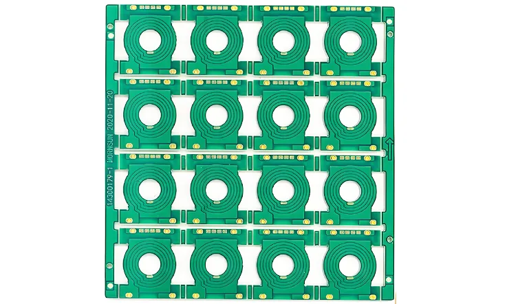
●Panelization: Planning the panelization scheme early is advisable. Clear instructions for V-scoring or tab routing, including placement of tooling holes and fiducials, should be provided.
Drilling and Plating Considerations
Reliable interconnects are built upon sound drilling and plating practices.
●Aspect Ratio: The via aspect ratio (board thickness divided by the smallest drill diameter) must be considered. High aspect ratios (>10:1) are more challenging to plate reliably; consultation regarding specific capabilities is recommended.
●Via-in-Pad: If using via-in-pad designs, they should be specified as filled and capped (plated over). This action prevents solder wicking during assembly and creates a reliable, planar surface for component mounting.
●Thermal Reliefs: Using thermal relief pads when connecting pads or vias to large copper planes allows for proper heat flow during soldering, preventing cold joints.
Solder Mask and Silkscreen
These final layers are for assembly and identification.
●Solder Mask Dam: A sufficient solder mask “dam” (webbing) between fine-pitch component pads helps prevent solder bridging during assembly.
●Clearances: Adequate clearance between silkscreen markings and solderable pads prevents ink from contaminating the pads.
● Via Tenting: A design should specify whether vias will be tented (covered with solder mask), plugged (filled with mask), or left open.
Ready to ensure your design is optimized for manufacturing? Submit your files for a complimentary DFM analysis.
Advanced Thermal Management Strategies with N4000-29
As component densities and power consumption increase, thermal management becomes a demanding design discipline. Nelco N4000-29’s favorable thermal properties provide a strong foundation, but effective heat dissipation requires deliberate design strategies.
Application of Thermal Vias
Thermal vias are a primary mechanism for conducting heat away from components.
●Placement: An array of thermal vias should be placed directly under the thermal pads of high-power components (e.g., QFNs, power FETs).
●Design: Thermal vias should have as large a diameter as practical and connect directly to a large ground or power plane on an inner or outer layer, which then acts as a heat spreader.
●Effectiveness: The effectiveness of thermal vias is proportional to the total copper cross-sectional area. Using multiple vias is more effective than relying on a single one.
Integration of Embedded Coins and Heatslugs
For the most demanding applications, more aggressive thermal solutions may be specified.
●Copper Coins: A solid copper coin can be embedded into a cutout in the PCB, directly beneath a high-power component. This provides a highly efficient, direct thermal path from the component to a chassis or external heatsink.
●Press-Fit Heatslugs: Similar to coins, these are metal slugs that can be pressed into the board post-fabrication. They offer an excellent thermal interface for components generating extreme localized heat.
●Fabrication Complexity: These technologies require advanced fabrication techniques, including precise milling, depth control, and specialized lamination cycles, yet offer unparalleled thermal performance.
Surface Heatsinking and Conduction Cooling
Using the board itself as part of the thermal solution is a cost-effective strategy.
●Copper Pours: Maximizing the use of large, solid copper planes on the outer layers, especially around hot components, allows the copper to act as a heat spreader, reducing localized hot spots.
●Chassis Grounding: In systems with a metal enclosure or chassis, using multiple mounting holes with plated perimeters tied directly to the ground planes allows the chassis to function as a large heatsink for the entire board.
Facing a complex thermal challenge? Consult with an engineer on advanced cooling solutions.
Power Distribution Network (PDN) Design and Optimization
A stable, low-impedance Power Distribution Network (PDN) is just as fundamental as signal integrity for reliable high-speed performance. The PDN must supply clean, steady voltage and current to active devices under all operating conditions.
Understanding Target Impedance
The objective of PDN design is to maintain a low impedance across a wide frequency range.
●Transient Current: When digital components switch, they demand a sudden, large burst of current. If the PDN has high impedance, this current draw causes a voltage drop (noise), which can compromise performance.
●Frequency-Dependent Impedance: The impedance of the PDN changes with frequency. The design goal is to keep this impedance below a calculated target value from DC up to the gigahertz range.
Decoupling Capacitor Strategy
Capacitors are the primary tool for managing PDN impedance.
●Bulk Decoupling: Larger capacitors (10-100μF) are used to supply low-frequency current and stabilize the voltage regulator module (VRM).
●Ceramic Decoupling: Smaller ceramic capacitors (0.1μF, 0.01μF) should be placed as close as physically possible to the power pins of every active device. These supply the high-frequency transient currents.
●Mounting Inductance: The effectiveness of a decoupling capacitor is limited by its mounting inductance. Using short, wide traces and connecting directly to the power/ground planes via multiple vias minimizes this inductance.
Leveraging Embedded Capacitance Planes
The PCB structure itself can be used as a high-frequency capacitor.
●Plane Capacitance: By placing a power plane and a ground plane very close together (using a thin Nelco N4000-29 prepreg layer), a parallel-plate capacitor is created.
●Benefits: This embedded capacitance provides extremely low inductance and is effective at suppressing noise at very high frequencies (above 500 MHz), where discrete capacitors become less effective.
●Implementation: This technique is highly effective in Nelco N4000-29 builds due to its ability to be reliably fabricated with very thin dielectric layers.
RF and Microwave Circuit Design Considerations
Nelco N4000-29’s stable electrical properties make it a suitable choice for many RF and microwave applications. Specific design techniques are required to maximize its performance in this domain.
Transmission Line Structures
The choice of transmission line influences performance and manufacturability.
● Microstrip: Easiest to fabricate, but is unshielded and prone to radiation. Best for non-sensitive RF lines.
● Stripline: Offers excellent shielding and isolation as the trace is “buried” between two ground planes. This is the preferred structure for sensitive RF traces, filters, and couplers.
● Coplanar Waveguide (CPW): Can offer very good performance and isolation, especially when grounded (GCPW). It keeps the signal and its return path on the same layer, simplifying layer transitions.
Implementing Passive RF Structures
The physical layout of copper defines the function of many RF components.
● Filters: The resonant frequency and bandwidth of printed filters (e.g., edge-coupled, hairpin) are highly dependent on the material’s Dk. The stability of N4000-29’s Dk ensures predictable filter performance.
● Couplers and Dividers: Structures like Lange couplers and Wilkinson power dividers rely on precise geometric control of line widths and spacing. The excellent fabrication tolerances achievable with N4000-29 are beneficial here.
● Phase Matching: In phased-array antennas and other phase-sensitive circuits, trace lengths must be precisely matched. The material’s uniform Dk ensures that electrical length corresponds directly to physical length.
Grounding and Shielding for RF Isolation
Preventing unwanted coupling between RF circuits is a design necessity.
● Via Stitching: Creating a dense “picket fence” of ground vias around the perimeter of RF circuits and along the edges of coplanar waveguides results in a virtual shielded box, containing electromagnetic fields.
● Shielding Cans: Designing pads on the PCB for soldering on metal shielding cans provides a high degree of isolation for sensitive circuits like local oscillators (LOs) or low-noise amplifiers (LNAs).
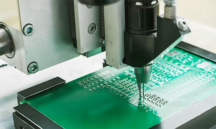
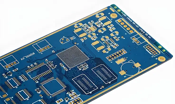
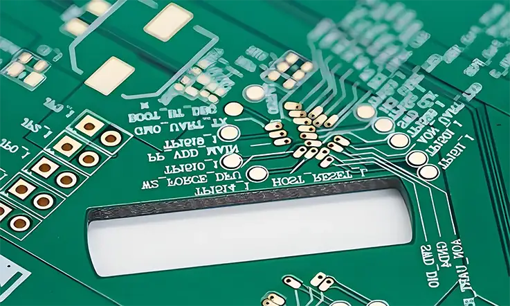
The Fabrication Process: From CAM to Bare Board
This stage transforms digital design files and raw materials into a physical, high-precision multilayer bare board. The process is a sequence of meticulously controlled chemical and mechanical steps.
Pre-Production and Tooling
●CAM Engineering: Engineers use advanced CAM software to panelize a design, add fabrication-specific features (tooling holes, coupons), and run DFM checks.
●Impedance Modeling: Trace widths and dielectric spacing are fine-tuned in the CAM data using a field solver to ensure the final product meets specified impedance targets.
Inner Layer Processing
●Imaging: Inner layer cores are imaged with circuit patterns using high-resolution Laser Direct Imaging (LDI) technology.
●Etching: The unwanted copper is chemically etched away, leaving the desired trace and pad patterns.
●AOI (Automated Optical Inspection): Every inner layer is scanned by an AOI machine to verify it is 100% free of shorts, opens, or other defects.
Lamination and Drilling
●Lay-up: The inspected inner layers and layers of Nelco N4000-29 prepreg are stacked together in a precise alignment.
●Lamination: The stack is placed in a large lamination press, where immense pressure and high temperature are applied to cure the prepreg and bond the layers into a single solid board.
●Drilling: High-speed CNC drills create all the plated through-holes (vias). For HDI boards, precision lasers are used to drill the tiny microvias.
Plating and Outer Layer Definition
●Electroless Copper: A thin layer of conductive copper is deposited in the drilled holes, a foundational step for layer-to-layer connection.
●Outer Layer Imaging & Plating: The outer layers are imaged, and then additional copper is electroplated onto the traces, pads, and into the via barrels.
●Final Etch: The remaining unwanted foil on the outer layers is etched away, defining the final circuit pattern.
The Assembly Process: From Solder Paste to Final Product
The assembly stage (PCBA) populates the bare board with electronic components, bringing the design to life. This stage requires absolute precision to maintain the board’s designed performance.
Solder Paste Application and Inspection
●Stencil Printing: A custom stainless-steel stencil is used to apply solder paste to the component pads on the bare board with high precision.
●3D SPI (Solder Paste Inspection): Immediately after printing, an automated 3D SPI machine inspects 100% of the solder paste deposits, verifying correct volume, height, area, and alignment to prevent soldering defects before they happen.
Component Placement
●SMT Placement: High-speed, high-accuracy pick-and-place machines use vision systems to rapidly place surface-mount technology (SMT) components onto the solder paste deposits.
●Component Variety: The assembly lines accommodate a huge range of components, from large connectors to fine-pitch BGAs and tiny 01005 passive devices.
●Through-Hole and Manual Assembly: For through-hole components or other parts that cannot be machine-placed, skilled technicians perform manual insertion and selective soldering.
Soldering and Cleaning
●Reflow Soldering: The populated board passes through a multi-zone convection reflow oven. A custom thermal profile is created for each assembly to ensure all solder joints are formed perfectly without overheating the board or its components.
●Wave Soldering: For boards with a high density of through-hole components, a wave soldering process may be used.
●Cleaning: After soldering, boards can be passed through an aqueous cleaning process to remove flux residues, a procedure for high-reliability and RF applications.
Value-Added Services: Beyond Assembly
The commitment to a project’s success extends beyond manufacturing and assembly. A suite of value-added services can deliver a fully tested, protected, and deployment-ready product, streamlining the supply chain and reducing time to market.
Conformal Coating Services
Conformal coating is a protective polymer film applied to the PCB assembly to shield it from environmental hazards.
●Protection: It protects sensitive electronics from moisture, dust, chemicals, and temperature extremes, enhancing long-term reliability.
●Coating Types: Various types of coating can be offered to suit different applications, including Acrylic (general purpose), Urethane (excellent chemical resistance), and Silicone (best for high-temperature environments).
●Application Methods: Capabilities may include automated spray coating for high-volume work, selective coating to mask off specific areas like connectors, and precision manual coating for complex assemblies.
Functional Testing (FCT) and Programming
Verifying that a product works as designed is a final confirmation of quality.
●Test Fixture Development: A collaborative effort with a client or their designated test engineering firm can develop and build custom functional test fixtures (“bed of nails”).
●Firmware Flashing and Programming: Services can include flashing firmware, programming microcontrollers, and loading serial numbers or MAC addresses onto the boards as part of the assembly process.
●Testing Services: Technicians can execute FCT protocols, providing pass/fail data for every unit and helping to diagnose any failures.
Rework and Repair Services
For high-value assemblies, expert rework can offer significant cost savings.
●BGA Rework: Specialized BGA rework stations with split-vision optics allow for the precise removal and replacement of complex Ball Grid Array components.
●Fine-Pitch Component Repair: Highly skilled technicians can perform delicate rework on fine-pitch SMT components, including trace repair and pad restoration.
●Certified Technicians: Rework should be performed by technicians certified to IPC standards, ensuring the highest level of quality and reliability.
Quality Assurance and Reliability Testing Protocols
Quality is not a final inspection; it is a philosophy embedded in every step of the process. A multi-layered approach to verification ensures every product meets or exceeds industry standards like IPC-A-600 Class 2 or Class 3.
In-Process Quality Control (IPQC)
●Microsection Analysis: Routinely, cross-sectional analysis is performed on coupons from the production panel. This allows for visual inspection of plating thickness, layer registration, lamination quality, and hole wall integrity under a high-power microscope.
●Process Monitoring: All chemical baths (etching, plating) and mechanical processes (lamination, drilling) are constantly monitored and controlled via Statistical Process Control (SPC).
Bare Board Electrical and Physical Testing
●100% Electrical Test: Every bare board is tested for opens and shorts using either a flying probe or bed-of-nails tester, guaranteeing its electrical integrity matches the netlist.
●TDR Testing: For controlled impedance boards, Time-Domain Reflectometry (TDR) testing is performed on on-panel coupons to provide empirical proof that the impedance values are within the specified tolerance.
●Dimensional Inspection: Automated systems verify hole sizes, board dimensions, and overall physical conformance to the fabrication drawing.
Assembly-Level Inspection
●Post-Reflow AOI: Every assembled board is scanned by a 3D AOI machine to verify correct component placement, polarity, and solder joint quality.
●X-Ray Inspection: For components with hidden solder joints like BGAs and QFNs, 2D and 3D X-ray inspection is used to see through the component and verify solder joint integrity, checking for voids, bridges, and other hidden defects.
Have stringent quality or reliability requirements? Request a sample quality report or discuss your specific testing needs.
Reliability Engineering and Failure Analysis
For industries where failure has severe consequences, standard quality assurance is not enough. A Design for Reliability (DfR) philosophy and the capabilities for in-depth failure analysis are needed to ensure a product survives its intended operational life.
Understanding Common Failure Modes
A proactive approach to reliability starts with understanding potential weaknesses.
●Via Fatigue (Barrel Cracking): Caused by Z-axis CTE mismatch, this is a known failure mode in thermal cycling. The low CTE of N4000-29, combined with robust plating processes, directly mitigates this risk.
●Conductive Anodic Filament (CAF): An electrochemical process that can cause shorts between vias. The high CAF resistance of N4000-29 is an advantage for long-life, high-density products.
●Pad Cratering: A fracture that occurs under a BGA pad during mechanical or thermal stress. Best practices in material selection and assembly can minimize this risk.
An Approach to Root Cause Analysis (RCA)
When failures do occur, a systematic approach to finding the root cause is required.
●Comprehensive Toolkit: A failure analysis lab can utilize a range of tools, including high-magnification microscopy, cross-sectioning, X-ray inspection, and electrical characterization.
●Systematic Process: A disciplined RCA process can isolate the failure, identify the mechanism, and determine the underlying cause, whether it’s related to design, material, or process. This leads to effective and permanent corrective actions.
Designing for Long-Term Reliability (DfR)
Building reliability into a design from the start is the most effective approach.
●Physics of Failure: Understanding the physics behind potential failure mechanisms allows for informed design choices.
●HALT/HASS: Robust assemblies can be provided to support Highly Accelerated Life Testing (HALT) and Highly Accelerated Stress Screening (HASS) protocols, helping to identify design weaknesses early.
Engineering Hybrid PCBs: Integrating N4000-29 with Other Materials
A hybrid or mixed-dielectric PCB, which combines Nelco N4000-29 with other materials like standard FR-4 or specialized RF laminates, is a powerful strategy for optimizing both performance and cost.
Common Hybrid Stack-up Configurations
| Configuration Type | Material Usage | Key Application Areas |
| RF/Digital Hybrid | Rogers (outer layers) + N4000-29 (inner layers) | Antennas, filters, high-speed digital |
| Performance/Cost Hybrid | N4000-29 (critical signal layers) + FR-4 (power/ground planes) | Cost-sensitive high-speed designs |
● RF/Digital Hybrid: A common configuration places a low-loss RF material (like a Rogers laminate) on the outer layers for antenna or filter performance, while using Nelco N4000-29 for the inner layers carrying high-speed digital signals.
● Performance/Cost Hybrid: For cost-sensitive but high-performance designs, N4000-29 can be used for the high-speed signal layers, while standard FR-4 materials are used for the non-critical power and ground planes.
Fabrication and Lamination Challenges
Building hybrid boards requires deep process expertise.
●Dissimilar Material Properties: Each material has a different CTE, resin flow characteristic, and optimal lamination temperature. The lamination cycle must be carefully engineered to be compatible with all materials in the stack-up to ensure a void-free, reliable bond.
●Hole Wall Preparation: The process for preparing the drilled hole walls for plating (desmear) can be different for different materials. A process must be used that effectively prepares all exposed dielectrics without damaging any of them.
●Sequential Lamination: Many complex hybrid designs require sequential lamination, where subsets of layers are laminated and processed first, and then additional layers are added in a second or even third lamination cycle. This requires extremely precise registration control.
Benefits of the Hybrid Approach
●Targeted Performance: This approach allows a designer to use the best-performing material exactly where it is needed, without paying a premium for the entire board.
●Cost Optimization: It can substantially reduce the total material cost of a board compared to using the most expensive material throughout the entire stack-up.
●Design Flexibility: It opens up new possibilities for integrating different types of circuitry onto a single, compact PCB.
Planning a mixed-material design? Discuss your hybrid stack-up with a fabrication specialist.
Applications and Industry Case Studies
Nelco N4000-29’s balanced performance profile makes it a frequently selected material across numerous demanding industries where reliability and signal integrity are non-negotiable.
Telecommunications and Networking
●Application: High-speed backplanes, line cards, and switch fabric boards for core routers and switches.
●Reasoning: Its low loss is beneficial for transmitting data at rates of 28 Gbps, 56 Gbps, and higher across large boards. Its thermal stability allows it to survive the assembly of large, high-thermal-mass connectors and operate reliably in thermally dense chassis.
Aerospace and Defense
●Application: Avionics control systems, radar and communication modules, and electronic warfare systems.
●Reasoning: It offers extreme reliability through thermal cycling and vibration. Its CAF resistance is beneficial for long-life missions in potentially humid environments. Its stable electrical properties ensure consistent performance of navigation and communication circuits.
Automotive and Electric Vehicles (EV)
●Application: Advanced Driver-Assistance Systems (ADAS) sensor fusion modules, EV battery management systems (BMS), and powertrain control units.
●Reasoning: It provides the thermal robustness to survive harsh under-hood operating conditions. Its stable dielectric properties are needed for processing high-speed sensor data reliably.
Test and Measurement:
●Application: Probe cards for semiconductor testing, ATE load boards, and high-frequency test fixtures.
●Reasoning: It provides a stable, low-loss platform for testing high-speed devices, ensuring that the test fixture itself does not corrupt the measurement. Its mechanical stability is beneficial for maintaining precise alignment in probe applications.
Comparative Analysis: N4000-29 vs. Competing Laminates
Choosing the right laminate requires balancing performance, cost, and manufacturability. Here is how Nelco N4000-29 compares against common alternatives.
N4000-29 vs. Standard FR-4
| Comparison Factor | N4000-29 | Standard FR-4 |
| Dielectric Constant (Dk) | ~3.7 @ 10 GHz | ~4.2–4.5 @ 1 MHz |
| Dissipation Factor (Df) | ~0.008 @ 10 GHz | ~0.020–0.025 @ 1 MHz |
| Glass Transition Temp (Tg) | >210°C | ~130–170°C |
| Decomposition Temp (Td) | >380°C | ~300°C |
| Cost | Moderate to High | Low |
●Performance: N4000-29 offers substantially lower signal loss (Df), a more stable dielectric constant (Dk), and much higher thermal stability (Tg, Td) than any standard FR-4.
●Cost: It is more expensive than FR-4, but this cost is often justified for applications with signal speeds above ~2-3 Gbps or operating in high-temperature environments.
●Selection Guidance: Choose N4000-29 when FR-4 fails to meet signal integrity or thermal reliability requirements.
N4000-29 vs. “High-Performance” FR-4 (e.g., FR408HR)
| Comparison Factor | N4000-29 | FR408HR (Example) |
| Dielectric Constant (Dk) | ~3.7 @ 10 GHz | ~3.6–3.8 @ 10 GHz |
| Dissipation Factor (Df) | ~0.008 @ 10 GHz | ~0.012 @ 10 GHz |
| Glass Transition Temp (Tg) | >210°C | ~180–200°C |
| Decomposition Temp (Td) | >380°C | ~340–360°C |
| Cost | Comparable | Comparable |
●Performance: This is a closer comparison. Materials like Isola’s FR408HR offer similar high thermal performance. However, N4000-29 typically maintains a slight edge in lower signal loss (Df) and electrical stability across frequency.
●Cost: Costs are often comparable, making the choice dependent on specific electrical performance needs and supply chain availability.
●Selection Guidance: Choose N4000-29 when needing the best electrical performance within the high-performance epoxy class of materials.
N4000-29 vs. Ultra-Low-Loss RF/Microwave Laminates (e.g., Rogers RO4350B)
●Performance: Materials like Rogers RO4350B offer even lower signal loss, making them the standard for very high-frequency RF applications (>20 GHz). However, their thermal properties (specifically Z-axis CTE) can be more challenging in high-layer-count builds.
●Cost: N4000-29 is substantially more cost-effective than most Rogers materials.
●Selection Guidance: Choose N4000-29 for applications up to ~15-20 GHz where the exceptional performance of a Rogers material is not strictly necessary, or in hybrid builds to control cost.
Cost-Performance Analysis: Finding the Economic Sweet Spot
The true cost of a PCB extends beyond the price of the bare board. A proper analysis considers the Total Cost of Ownership (TCO), which includes factors like fabrication yield, assembly success, field reliability, and potential redesign costs.
Beyond Material Cost: The Value of Reliability
●Fabrication Yield: N4000-29’s robust manufacturability often leads to higher yields on complex designs compared to more exotic materials, reducing scrap and lowering the effective price per board.
●Assembly Success: Its thermal stability reduces the risk of assembly-related failures like delamination or pad lift, saving on costly rework and repair.
●Field Reliability: A single field failure can have costs far exceeding the price of the entire PCB. Investing in a reliable material like N4000-29 is a form of insurance against costly product recalls and warranty claims.
Defining Crossover Points
●Upgrading from FR-4: The crossover point is typically when signal loss over a given trace length becomes unacceptable, or when the operating temperature or number of reflow cycles exceeds the limits of FR-4.
●Choosing N4000-29 Instead of Premium RF Materials: The crossover point is when the marginal improvement in signal loss offered by a more expensive material does not provide a functional benefit to the system, or when budget constraints are primary and N4000-29’s performance is sufficient.
Material Handling and Storage Protocols
Proper handling and storage of high-performance laminates like Nelco N4000-29 are foundational to ensuring their performance is not compromised before fabrication begins.
Moisture Sensitivity and Bake-Out
●Hygroscopic Nature: All epoxy-based systems are hygroscopic, meaning they can absorb moisture from the atmosphere. This trapped moisture can cause catastrophic delamination during the high temperatures of lamination or reflow.
●Storage: All raw laminates and prepregs must be stored in a climate-controlled environment (typically <25°C, <50% RH) and must remain in their original vacuum-sealed packaging.
●Bake-Out Procedures: If material has been exposed to ambient conditions for an extended period, a pre-fabrication bake-out cycle (e.g., 4-6 hours at 120°C) is required to drive out any absorbed moisture.
In-Process Handling
●Cleanliness: All handling must be done in a clean environment. Oils, dust, and other contaminants on the surface of the laminate can lead to poor adhesion, delamination, or electrical defects.
●ESD Precautions: While the laminate itself is an insulator, proper ESD (Electrostatic Discharge) protocols must be followed in any area where electronic designs are being handled.
A Collaborative Engineering Engagement
Every project is approached as a technical engagement. The objective is to work with designers from the earliest stages to ensure a successful outcome. The collaborative process is designed to be transparent, supportive, and efficient.
Phase 1: Initial Design Consultation
●DFM/DFA Review: The process begins with the submission of design files. An engineering review identifies any potential optimizations for manufacturability, cost, or reliability.
●Material and Stack-up Support: Assistance can be provided to select the optimal materials and design a robust, cost-effective stack-up tailored to specific performance requirements.
Phase 2: Prototyping and Validation
●Production-Grade Prototypes: Prototypes can be fabricated using the exact same materials and processes as full-scale builds, ensuring that validation testing is meaningful.
●Rapid Turnaround: Expedited turnaround times for prototypes can accelerate development and test cycles.
Phase 3: Scaling to Volume
●Seamless Transition: Once a design is validated, a seamless transition to volume quantities can occur using the same tooling and process parameters, ensuring consistency from the first board to the last.
●Supply Chain Management: The material supply chain can be managed to ensure a steady, reliable source of Nelco N4000-29 and other required components for a production run.
Ready to move from design to delivery? Initiate your project quote today.
Frequently Asked Questions (FAQs)
Q: Can N4000-29 be used with heavy copper for high-power applications?
A: Yes, N4000-29 is compatible with heavy copper weights (e.g., 3 oz or 4 oz). Its thermal stability helps maintain laminate integrity during the thermal cycling of heavy copper boards.
Q: How many lead-free reflow cycles can a typical N4000-29 board withstand?
A: Due to its high Tg and Td values, a well-fabricated N4000-29 board can typically withstand 5-6 lead-free reflow cycles without delamination or thermal damage.
Q: What is the typical impedance control tolerance achievable on N4000-29 boards?
A: A standard impedance tolerance of ±7% is consistently achievable. With tighter process controls for specific designs, tolerances of ±5% can be attained.
Q: Is N4000-29 suitable for sequential lamination cycles?
A: Yes, it is well-suited for sequential lamination. Its excellent dimensional and thermal stability allow it to maintain precise layer-to-layer registration through the multiple lamination cycles required for complex HDI builds.
Q: What are the main considerations when bonding N4000-29 to PTFE-based materials?
A: The primary considerations are the CTE mismatch and lamination profile compatibility. This requires specialized bonding films and a precisely controlled lamination cycle engineered for both material types.
Q: How does N4000-29 perform when used for buried capacitance layers?
A: It performs excellently. Its uniform dielectric thickness control and stable dielectric constant allow for the creation of reliable buried capacitance layers with predictable capacitance values for high-frequency decoupling.
Q: What are the minimum line/space features achievable on N4000-29 using LDI?
A: With LDI (Laser Direct Imaging) and fine-tuned etching processes, line and space features of 3/3 mil (0.075mm / 0.075mm) are consistently achievable to meet high-density design requirements.


