
Plated through holes (PTH) play a crucial role in connecting traces and components across multilayer PCBs, while facilitating electrical connections between layers. PTHs are a reliable and versatile choice for mechanical and mounting needs.
However, a potential issue lies in the manufacture of PTHs. In some cases, it may not be necessary to have the via extend through the entire board. The unfinished section, referred to as a stub, does not contribute to the circuit’s functionality and can create signal distortion, particularly in high signal level circuits.
For production purposes, incorporating backdrilling in the fabrication of multi-layer circuit boards presents an effective solution. Backdrilling serves to mitigate issues related to deterministic jitter, high bit error rates, signal attenuation, and electromagnetic interference.
Compared to buried and blind vias, backdrilling is a more cost-effective and efficient approach for multilayer boards. While buried and blind vias require distinct drilling and plating processes, drilling and plating through all layers of the board before backdrilling is a superior cost-effective option. With this technique, problematic stubs in PTH can be removed effectively.
Therefore, the use of backdrilling is an effective method to rid PTHs of problematic stubs for multilayer circuit boards, thereby enhancing signal quality and improving overall circuit stability.
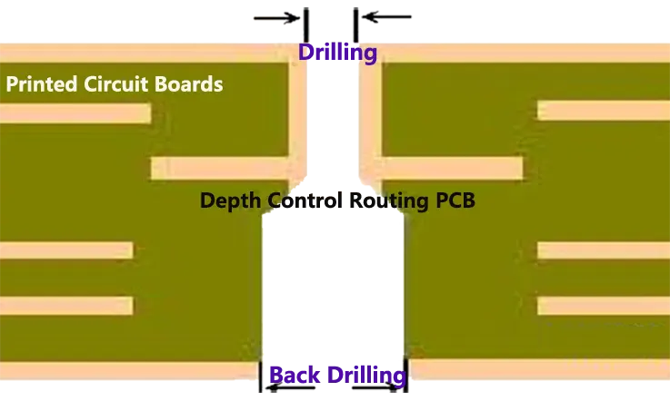
Definition of Back Drilling and Controlled Depth Drilling
The design of high-speed printed circuit boards (PCBs) poses challenges in maintaining signal integrity, but these challenges can be addressed by adhering to appropriate manufacturing and design standards. One problem that occurs in high-speed design is the presence of via stubs which are non-functional components of a via that can cause signal reflection and interfere with intended transmission. To overcome this problem, back drilling can be carried out, which involves removing the majority of the via stub by using a slightly larger diameter drill bit during the second round of drilling.
When back drilling, a hole that is only slightly bigger in diameter than the plated through hole (PTH) is drilled to remove the conductive via stub and reduce its length to 10 mils or less to avoid signal reflections. Controlled depth drilling is a feasible solution for any type of PCB with stubs that induce signal degradation and involves minimal design and layout considerations. However, when using blind vias, the aspect ratio needs to be taken into account.
After the PCB fabrication process, holes with stubs are redrilled using a slightly larger drill to remove the unnecessary stubs. The holes are then back drilled to a controlled depth, stopping just short of making contact with the layer previously utilized by that route.
So, controlled depth drilling and back drilling can help resolve signal integrity issues related to via stubs in high-speed PCB design. These techniques provide a practical solution for PCB manufacturers to improve signal quality and prevent signal reflections, making them a critical component in high-speed circuit design.
Back Drilling of PCB Boards : Advantages and Disadvantages and Features
Back drilling is a technique used in printed circuit board (PCB) design to remove excess material from vias that are non-functional, referred to as stubs, which can cause signal reflections and degradation of transmission quality in high-speed PCBs. Here are some advantages, disadvantages, and features of back drilling:
Advantages
● Improves signal integrity: By removing the excess material in via stubs, back drilling reduces signal reflections and maintains signal integrity, improving the overall performance of the PCB.
● Cost-effective: Back drilling uses a simple process that is less expensive than other solutions, such as the use of blind or buried vias.
● Easy to implement: Back drilling is easy to implement, requires minimal design and layout considerations, and can be applied to any PCB with stubs that cause signal degradation.
● No impact on other layers: The back drilling process only removes material from the unwanted via stubs, and does not affect the other layers of the PCB.
● Wide range of applications: Back drilling can be used in a wide range of high-speed PCB applications, such as server systems, telecommunications, and high-frequency circuits.
Disadvantages
● Reduced mechanical strength: Back drilling may decrease the mechanical strength of the PCB at the locations of the removed via stubs, which can be a concern in applications where mechanical stress or vibration is present.
● Requires additional manufacturing steps: Back drilling requires an additional manufacturing step, which may increase the manufacturing time and costs.
● Limits the number of back drills: There is a limit to the number of back drills that can be performed on a single via before it is rendered ineffective.
Features
● Controlled depth: Back drilling is a controlled depth drilling process, which ensures removal of excess material from the via stubs without affecting the other layers of the PCB.
● Small tolerance: The drill bit used in back drilling has a small tolerance to ensure that it removes only the excess material from the via stubs and does not damage the other layers of the PCB.
● Reduces EMI: Back drilling reduces electromagnetic interference (EMI) in high-speed PCBs, leading to better signal quality and reducing the probability of missed signals.
● Enables higher frequencies: By removing signal reflections, back drilling allows for the use of higher frequencies in the PCB without signal degradation.
Back Drilling vs. Vias
Back drilling and vias serve similar functions in PCB design, which is to connect multiple layers of a printed circuit board. However, back drilling and vias differ in some aspects.
● Vias are small plated-through holes in the PCB that provide a path for electrically connecting two or more conductive layers of a PCB. They create electrical connections between the layers and can also be used to dissipate heat, reduce ground loops, and for mechanical support.
● Back drilling, on the other hand, is specifically used to remove unused via stubs that can cause signal reflection and signal integrity issues. Back drilling helps ensure high-speed and reliable data transmission by optimizing signal integrity.
● While both technologies are necessary for different reasons, back drilling is particularly important with some high-frequency and high-speed applications where timing and signal integrity are critical.
In a words, both vias and back drilling play a critical role in PCB design. They may be used together when appropriate, but for high-speed PCB designs, back drilling may be the preferred option since it reduces noise, signal reflection and improves signal quality.
Which PCBs Require Back Drilling?
● When there is a trace connected to via holes at the top or bottom layer of a PCB, stub bifurcation can occur, which leads to signal reflections and lower signal quality. This issue is particularly problematic for high-speed signals, such as those with a rate of ≥ 1 Gbps.
● To mitigate these issues and achieve high-quality signal transmission, it is essential to incorporate back-drill design into the circuit tracks on the PCB board. However, the design of high-speed interconnection lines requires system engineering expertise, and it is not a straightforward task. In some cases, if the chip’s drive capacity is strong enough or the system’s interconnection links are short, it might be possible to pass without the need for back-drill design.
Therefore, for a reliable solution, system interconnection link simulation is the most effective way to determine whether back-drilling is necessary. This simulation aids in identifying possible signal distortion issues and enables engineers to make the appropriate design choices to enhance signal quality and system performance.
● In addition to employing back drilling technology to remove via stubs and prevent signal reflections, PCB manufacturers can utilize various building techniques such as blind and buried vias, microvias, alternate stack-up arrangements, and trace relocation to reduce or eliminate via stubs. However, such alternatives are not always practical due to manufacturing limitations and cost considerations. For high-density PCBs or backplanes/mid-planes, removing via stubs by back drilling is often the most practical solution.
● When blind vias cannot be used due to the frequency of the board’s operation exceeding 1 GHz and less than 3 GHz, back drilling becomes necessary. In cases where PCBs contain numerous layers, some holes may not be designed as blind holes. For instance, in a 16-layer PCB, some via holes must connect with L1-10, while others need to connect with L7-16, making such holes unsuitable for blind design; instead, they are best designed as back drilled holes.
Therefore, while there are alternative methods for reducing via stubs on PCBs, back drilling is often the most rigorous and reliable, especially in high-density PCBs or backplanes/mid-planes where redesigning trace layouts is infeasible. Blind vias may not always be practical, and back drilling can be a necessary alternative for such cases.
Design Parameter of Back Drill Table
| Index | Type | Value min. |
| A | Back drilling Ø | 400µm |
| B | Plated-through via Ø | 200µm |
| C | Copper clearance | 150µm |
| D | Ø-Difference circumference | 100µm |
| E | Back drilling depth | 200µm |
| F | Distance to connected layer | see below |
| G | Thickness target layer | see below |
| H | Thickness stub remainder (safety) | see below |
Required Target Layer Thickness “G”
When requesting a specific layer buildup for printed circuit boards (PCBs), it is imperative to adhere to the minimum prepreg thickness of the layer where the drilling stops, as specified in the table below (G). This ensures that the necessary thickness calculations are factored in and the PCB meets the required specifications.
If a specific layer buildup is unnecessary, our PCB manufacturing process will perform all thickness calculations with reference to the thickness of “G.” This guarantees accuracy and consistency in the manufacturing process, thereby preventing errors and ensuring that the PCB meets all necessary standards and requirements.
| F ≤ 1.0mm | 1.0mm < F ≤ 2.0mm | 2.0mm < F ≤ 3.0mm | 3.0mm < F ≤ 4.0mm | |
| G min. | 250µm | 300µm | 400µm | 500µm |
| H | 125µm | 150µm | 200µm | 250µm |
| Tolerance | ± 100µm | ± 125µm | ± 175µm | ± 225µm |
Note:
● Gmin. = Thickness Target Layer.
● H = Distance To Connected Layer.
● Tolerance = Thickness Stub Remainder.
Important Design Considerations to Keep in Mind While Back Drilling
Here are some important design considerations to keep in mind while back drilling:
● Location: The location of the via stubs to be back drilled is important for the signal quality of the PCB. Via stub length and placement on the board need to be carefully considered to optimize signal integrity.
● Layer Thickness: The thickness of the layer may impact the back drilling process and its effectiveness. Layer thickness should be analyzed in relation to the drill bit being used to avoid any potential issues.
● Drill Bit Size and Type: Drill bit selection is essential to ensure via stubs can be accurately and efficiently removed. The selected drill bit must match the diameter of the concentrated copper pad of the vias being drilled.
● Manufacturing Capabilities: Back drilling requires advanced manufacturing capabilities, and it is essential to choose a manufacturer with a track record of delivering quality products. This ensures the manufacturer can provide the precision, accuracy, and consistency necessary for back drilling to be effective.
● Signal Integrity Analysis: Before designing the PCB, performing a thorough signal integrity analysis to determine if back drilling is needed is an essential step. This analysis helps identify signal weaknesses and locate excessive via stubs that should be back drilled.
Steps for a Back Drill Manufacturing Process
The back drilling process for producing printed circuit boards (PCBs) involves several critical steps to ensure successful manufacturing. These steps include:
● Use the locating holes provided on the PCB to precisely locate the first drilling holes on the board.
● Before electroplating, close the placement holes with a dry film to prevent electroplating in those areas.
● Electroplate the first drilled layer of the PCB.
● Transfer outer layer graphics onto the electroplated PCB.
● Perform graphic plating on the PCB once the outer layer pattern has been established.
● Before graphic plating, provide dry film sealing treatment on the placement hole to ensure the accuracy of the drilling.
● For back drilling, use the same placement hole as the initial drill.
● Back-drill the electroplated holes that require drilling to remove via stubs.
● Thoroughly clean the back drilling holes to remove any residual drill chips that may remain in the back-drilling process.
● Careful adherence to each of these steps is critical for proper back drilling of vias and achieving excellent signal integrity in high-speed PCB applications.
As a result, successful back drilling of PCBs for signal integrity requires precise location, dry film treatments, electroplating, graphic plating, and, most importantly, careful and thorough cleaning. These steps ensure that the PCB meets necessary industry standards and operates flawlessly in all applications.
Difficulties of Back Drilling process
● Back Drilling Depth Control: The technique of back drilling is utilized in PCB manufacturing to accurately process blind holes, wherein the depth control function of the drill bit is employed. The tolerance of this process is predominantly affected by the precision of the back drilling equipment, along with the precision of the thickness of the medium being drilled.
Achieving optimal results via back drilling method is reliant on appropriate drilling materials and procedures, as several external factors can influence its precision. These include the resistance of the drill bit, the angle of the drill bit, the contact effect between the cover plate and the measuring unit, and the warpage of the plate. Therefore, it is crucial to maintain a stringent approach to the production process that enables maximal control over the precision of the process.
● Back Drilling Precision Control: In the realm of PCB manufacturing, back drilling is achieved through secondary drilling, which is performed based on the diameter of the hole produced by the primary drilling process. The secondary drilling operation must be executed with an exceptional degree of accuracy, given its crucial influence on the quality control of the PCB during subsequent processing stages.
The precision of the equipment utilized in the back drilling process, the expansion and contraction of the board, and the method of punching can significantly impact the accuracy of the secondary drilling operation. As such, attaining an appropriate level of accuracy during secondary drilling via thorough and meticulous production procedures is paramount to uphold the quality and integrity of the final product.
Back-drilling PCB design: Notes and Common Problems
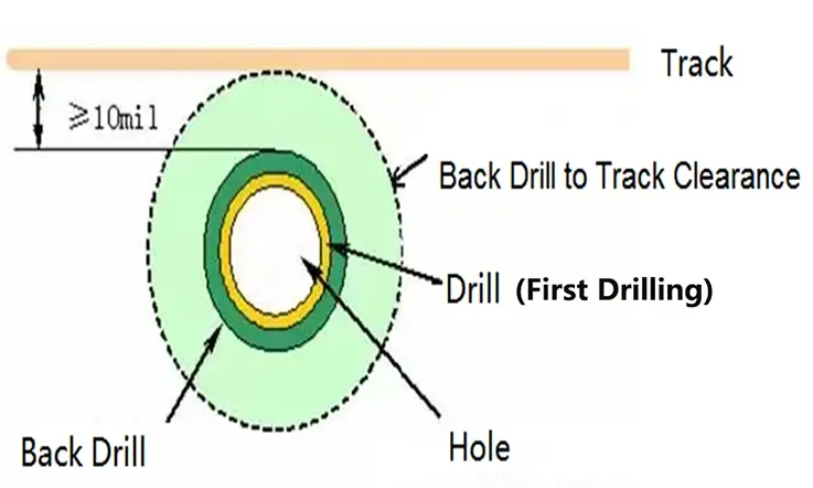
In PCB manufacturing, it is imperative to provide clear and concise instructions for outputting back-drill layers to the PCB board manufacturer. These instructions must include a specification detailing which layer corresponds to the layer requiring the matching back-drilling. Additionally, the size of the holes designated for reverse drilling must be greater than those for the initial drilling process, with a minimum back-drill size of 0.2 mm and hole-to-trace distance of 0.35 mm for the first drilling (0.2 mm for back-drilling).
When designing a PCB stack-up, it is essential to consider the dielectric thickness to prevent the trace from being drilled during the back-drilling process. If drilling to the “M” layer is required, a minimum of 0.2 mm of dielectric thickness (distance) must be maintained between the closest layer exempt from drilling and the “M” layer to ensure accuracy and consistency in the drilling process.
Here are some common back drilling issues that can arise during the PCB manufacturing process:
● Misaligned Drill Bit: If the drill bit is not properly aligned or is misaligned during the back drilling process, it can affect the signal integrity of the vias. This can cause crosstalk and interference with the adjacent vias.
● Breakout Voids: Breakout voids occur when the drill bit breaks through more layers than the intended number during the back drilling process. This can create copper protrusions that can short-circuit with adjacent traces, leading to signal integrity issues.
● Resin Smearing: During the back drilling process, resin may smear over the vias, which could lead to mechanical failures or affect the electrical performance of the PCB. Proper cleaning is imperative to remove any smearing effects.
● Thru-Hole Damage: Back drilling can cause the through-holes to break, which may lead to short circuits and signal integrity problems affecting PCB functionality.
● Uneven Back Drilling: Uneven back drilling can occur when the drill bit is not optimally positioned or when vibrations and other environmental factors occur. This asymmetry can cause difficulty in PCB assembly since pads may not provide enough support to have proper soldering.
To prevent these issues, it is important to perform proper quality control measures before, during and after the back drilling process. This includes monitoring the manufacturing process, testing the PCB thoroughly, and working with reputable manufacturers to ensure high precision and quality.
Application of Back Drilling
The back-drilling technique used for PCB production has found significant employment in various industries, including but not limited to communications hardware, aerospace, medical electronics, the military, and large servers.
● Network Communication Equipment: Back drilling is frequently used in network communication equipment such as routers, switches, and modems. These devices require high-speed data transmission with low signal reflection, which can be achieved through back drilling.
● High-Speed Computer Components: Back drilling can be used for high-speed computer components, including motherboards and graphics cards. This helps on achieving maximum speed and minimizing signal interference.
● Aerospace and Defense Systems: Aerospace and defense industries require high-speed, accurate, and reliable communication systems. Back drilling can ensure that their high-frequency circuits deliver optimal signal quality.
● Medical Devices: Medical devices in areas such as diagnostic imaging and other high-speed medical equipment require reliable data transmission, which can be ensured by back drilling.
● Automotive Electronics: Advanced driver-assistance systems (ADAS) and other vehicle systems require high-speed communication for proper operation and safety. Back drilling can be used to optimize signal integrity and ensure reliable communication reliability.
PCBs manufactured via back-drilling have demonstrated superior efficacy and reliability for use in diversified applications within these industries.
Recap of Back Drilling as an Essential PCB Design Technique
Back drilling is a crucial technique used in Printed Circuit Board (PCB) design and manufacturing. It involves removing unused via stubs that can cause signal integrity issues, leading to noise and reflection, and ultimately, affecting data transmission speeds.
Back drilling ensures high-quality and reliable data transmission by reducing signal reflections and noise, which is especially important for high-speed PCB designs. It is a cost-effective way to improve signal integrity and reduce the possibility of signal loss by removing unused via stubs.
Therefore, back drilling is an essential PCB design technique that ensures the highest possible performance level of the PCBs. It should be considered in all high-speed PCB designs to guarantee reliable and high-quality data transmission.
Conclusion
In the realm of PCB production, back drilling technology plays a vital role in removing unwanted solder mask stubs from the board surface. Without the use of a back drill, resolving problematic solder mask stubs can prove to be a challenging task, potentially leading to unfortunate signal crosstalk, among other issues. Therefore, back drilling technology is crucial for enhancing signal integrity on PCBs.
At JarnisTech, we are a one-stop PCB manufacturing and assembly factory situated in ShenZhen, China, specializing in a range of services, including PCB prototype and batch production, PCB assembly (SMT), PCB design, electronics module sales, CNC machining, and more. Our commitment to ensuring the highest quality, timely delivery, and cost-effectiveness for our clients’ requirements in the electronics industry is unwavering. We strive to meet the needs of producers worldwide across various sectors.
Related Posts:
1. What Is PCB Etching and How to Make a perfect PCB Etching?
2. The Best PCB Panelization Guide
3. The Importance of 3D Printed PCBs in Modern Electronics Production
4. Understanding PCB Delamination: A Comprehensive Guide
5. The Best Backplane Printed Circuit Boards Factory
6. An Overview of Through-hole Technology (THT)
7. Detail Talk Surface Mount Technology
8. PCB Clone : Copy Your Printed Circuit Board
9. PCB Drilling: Definition, Technology Types and Process
10. Castellation PCB Fabrication: Castellated Hole (Plated Half Hole) Technologys Why So Important


