
As a reputable PCB manufacturer, it is imperative to recognize that via protection is a crucial aspect of modern PCB design. Implementing this feature provides significant advantages throughout the production and assembly phases of PCB manufacturing, ultimately increasing the yield of acceptable finished products. By prioritizing the implementation of via protection in PCB design, manufacturers can ensure that their products meet or exceed industry standards, resulting in higher levels of customer satisfaction.
What Is a Via ?
In PCB manufacturing, plated through holes (PTHs), commonly referred to as vias, are utilized to establish the electrical connections between traces on different board layers. Due to their non-component lead installation function, the diameter of the holes and pads is usually on the smaller side. To achieve this goal, the two methods that are most commonly used in PCB manufacturing are outlined below. It is essential for PCB manufacturers to be knowledgeable about these methods to ensure the efficient production of high-quality printed circuit boards.
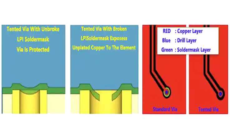
Soldermask Covered (Tented): 1
Solder resist, which is also referred to as Liquid Photo Imageable (LPI) ink, is a crucial component used in PCB manufacturing for via tenting. Via tenting requires designers to remove the solder mask opening from the via in their design by following a set of specified protocols. Standard practice entails using solder resist to cover a via’s annular copper ring, and this step does not impact the PCB’s cost.
Control over the outcome during this stage of the process is limited to whether or not the copper ring will be covered in solder resist ink. It is noteworthy that while the surface of the hole may be covered with solder resist ink, this is not a guaranteed result.
It is essential to note that the best possible results can be obtained by reducing the through hole size wherever possible. PCB designers should aim to choose a through hole that is equal or greater than 0.20mm in size. Via hole diameters smaller than 0.3 millimeters have the highest likelihood of being filled accurately, whereas filling results become less predictable when dealing with diameters between 0.3 and 0.5 millimeters. As the filling process is considered unregulated, it is not recommended for applications that require hole closure.
● Advantages: As a PCB design engineer, it is important to note that since via filling is conducted during the regular PCB process, it does not incur any additional costs. However, it is important to highlight that the screen printing process is an added cost. It is crucial to keep this in mind when designing PCBs and determining feasibility for specific projects. By considering the cost implications of each process, designers can make informed decisions that allow for cost-effective and efficient manufacturing processes.
● Disadvantages: While via filling is a useful technique, it may not be appropriate for all designs. For instance, it is not recommended for designs that require a filled-via percentage of exactly 100%. In such situations, an alternative technique would need to be utilized.
Moreover, via filling is not suitable for the Via In Pad technique, which is typically used for active via applications. Thus, it may not be recommended for use in highly complex designs that feature fine pitch Ball Grid Array (BGA) components. Engineers should consider these factors when planning PCB designs to ensure that they are selecting appropriate techniques that meet the specific requirements of each project.
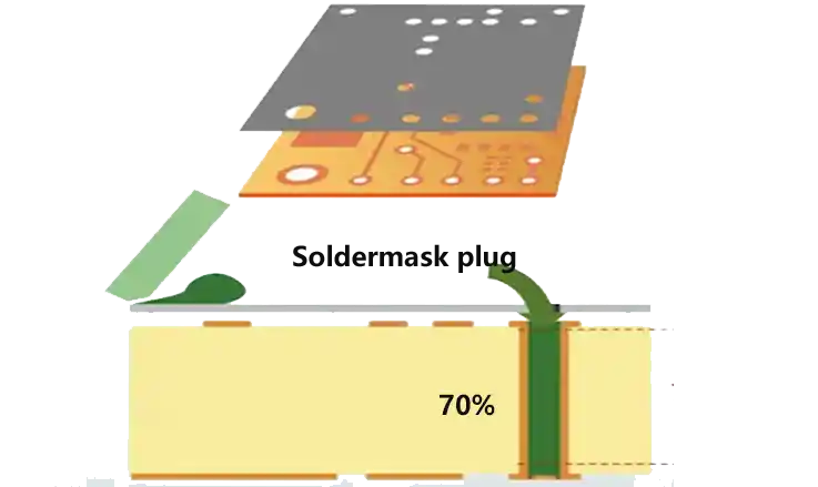
Soldermask Plug: 2
In PCB manufacturing, solder resist ink (LPI) can be utilized for filling via holes, similar to the process involved in tenting vias. This technique can be a useful solution for closing via holes in a PCB, which can improve its overall performance and reliability. It is important to consider various factors, such as hole size and location, when determining the feasibility of using this technique for any specific PCB project. By leveraging the appropriate tools and expertise, PCB manufacturers can achieve efficient and high-quality via filling as part of their overall manufacturing process.
In the via filling process, a drilled ALU sheet is employed to facilitate the injection of typical solder resist ink (LPI) into the via holes that require filling. Following this screen printing procedure, the standard solder mask technique can be carried out. The use of these techniques can provide exceptional results, with a one hundred percent success rate in most cases. It is important for PCB manufacturers to follow established best practices when performing these procedures to ensure that the via filling process is executed accurately and efficiently. By doing so, manufacturers can produce high-quality PCBs that meet the needs of their customers.
Screen Printing Process
● Advantages: When comparing the cost of via filling using solder resist ink (LPI) to the cost of through plugging processes, such as conductive or non-conductive plating, the former is generally less expensive. This makes via filling using LPI an excellent choice in situations where an absolute guarantee of filled vias is necessary.
Since the cost of via filling using solder resist ink is lower, it can be a more cost-effective option, especially when dealing with a large number of vias. It is important for PCB manufacturers to consider the specific requirements of each project and the associated cost implications when selecting a via-filling technique. This can help ensure that the chosen method is both effective and efficient, leading to high-quality results that meet the needs of their clients.
● Disadvantages: While via filling using solder resist ink (LPI) can be a suitable technique for certain PCB designs, it may not be appropriate for all situations. One example where it is not an appropriate choice is when utilizing the Via In Pad manufacturing method, which is commonly used for active via.
In such scenarios, alternative via-filling methods would need to be employed to ensure adequate coverage and optimal performance. PCB designers and manufacturers should be aware of these limitations when selecting a via filling method and should choose techniques best suited to the specific requirements of each project. By doing so, they can ensure that their PCBs are of high quality and meet their intended functionality.
Purpose of Via Protection
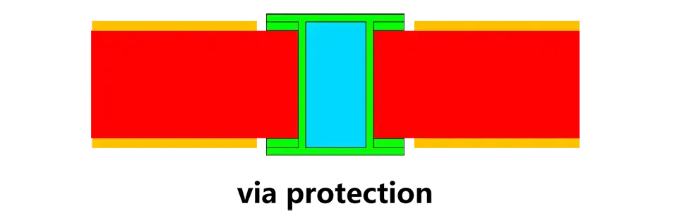
The purpose of via protection is to ensure reliable and robust electrical performance of printed circuit boards (PCBs) by protecting vias from damage or exposure to external elements. Via protection typically involves covering vias with materials such as solder mask, copper, or fill material to prevent the ingress of contaminants and improve their durability over time.
Via protection techniques can also help to maintain the electrical integrity of the circuit by preventing over-etching of vias during PCB fabrication, reducing the risk of signal loss, and interference. Additionally, via protection can help to reduce the likelihood of via failure due to factors such as thermal stress, mechanical stress, and electrostatic discharge (ESD) by improving the overall structural integrity of the via.
Via Protection Design Considerations
The design of via protection should be considered during the PCB layout and routing process. Some considerations for via protection design include:
● Trace routing: The placement and routing of PCB traces can affect the effectiveness of via protection techniques. For example, traces should not be routed close to the edge of a via that has been covered with solder mask to prevent the mask from peeling off or being damaged.
● Component placement: Components, especially those with high thermal dissipation, should not be placed too close to vias, as the heat generated by the component can damage the via or the via protection.
● Thermal management: High-temperature areas should be identified and proper thermal management techniques should be implemented to prevent thermal stress on vias. This can include designing vias with larger diameters to improve thermal conduction or implementing thermal relief patterns to reduce thermal stress.
● Mechanical stress: Vias that are exposed to mechanical stress, such as those located near the edges or corners of the PCB, should be reinforced with additional via protection to prevent damage.
● ESD protection: To prevent ESD damage to vias, additional protection such as overvoltage protection can be added to the design.
Considering these factors will ensure that via protection methods are applied effectively, resulting in reliable and robust PCB design.
Via Types
IPC-4761, also referred to as the Design Guide for Protection of Printed Board Via Structures, offers various strategies that can safeguard PCB vias. These approaches are classified into seven types:
● Type I (Tented): Covering the hole with a dry film solder mask that has been stretched over it, with no additional materials.
● Type II (Tented and Covered): Additional layer of dry film or a layer of liquid solder mask applied over the tented Type I via.
● Type III (Plugged): Partial insertion of a non-conductive material into the hole, which does not go all the way through.
● Type IV (Plugged and Covered): Additional layer of dry film or a layer of liquid solder mask used to cover the plugging of a Type III via.
● Type V (Filled): Complete filling of the hole with a conducting or non-conductive material that has penetrated all the way through.
● Type VI (Filled and Covered): Type V filled via masked using an additional layer of dry film or liquid solder mask.
● Type VII (Filled and Capped): Application of a metalized coating on top of the filled material in a Type V filled via.
In general, the production costs increase as you move down the list, with Type III being more expensive than Type I, and so on. PCB manufacturers should carefully evaluate the requirements of each project and select an appropriate via protection strategy that balances cost with functionality, ensuring that the end product meets the desired quality and reliability standards.
IPC-4761 Via Protection: Via Tenting, Via Plugging, Via Filling
To meet the technical and production-related requirements of PCB manufacturing, via protection is a crucial step that must be taken. There are several viable options available for covering vias, including:
● Completely Filled: Via Filling or Filled Vias.
● Partially Filled: Via Plugging or Plugged Vias.
● Simply Covering: Via Tenting or Tented Vias.
PCB manufacturers must consider the technical and production requirements of each project when selecting the appropriate via protection option to balance cost and functionality. This ensures that the final product is of high quality and achieves the desired level of reliability.
Via Tenting
● IPC-4761 Type I (Tented Via): A dry film solder mask stretched over the via hole without additional materials.
● IPC-4762 Type II (Tented & Covered Via): An additional layer of dry film or liquid solder mask applied over the tented Type I via.
Application
● Covering of critical vias, e.g. beneath BGA.
● Enables vacuum-adaption for production.
● Guard against solder paste that could float up to the component side.
Alternatives
One potential approach for protecting vias is through the use of the Via Filling method. This technique involves reducing the solder mask clearance, which can help ensure that BGAs are adequately covered by solder mask bridges. Through this method, some of the solder mask can be applied to the annular rings of the vias.
Parameters
| Covering | Max. Drill Diameter |
| Via Tenting | 0.3mm |
Designation
To achieve this, simply covering the vias with the solder mask layer is sufficient.
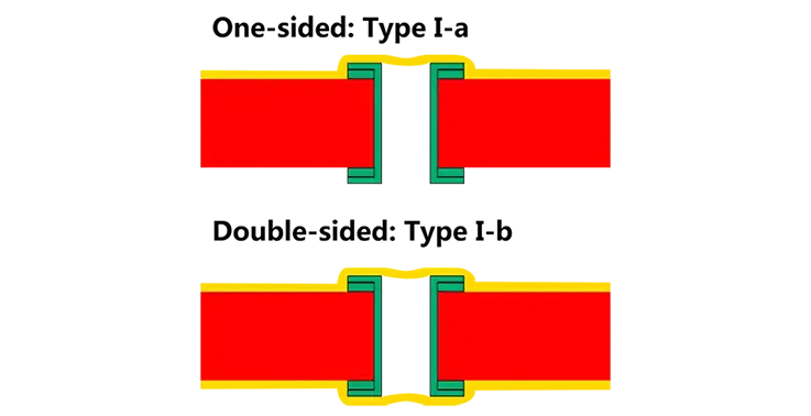
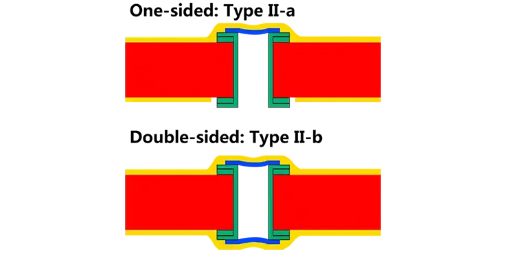
Via Plugging
● IPC-4761 Type III (Plugged Via): A non-conductive material partially inserted into the via hole, which does not extend to the other side.
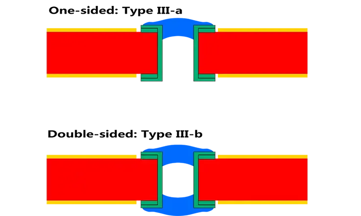
● IPC-4761 Type IV (Plugged & Covered Via): An additional layer of dry film or liquid solder mask applied over the plugged Type III via.
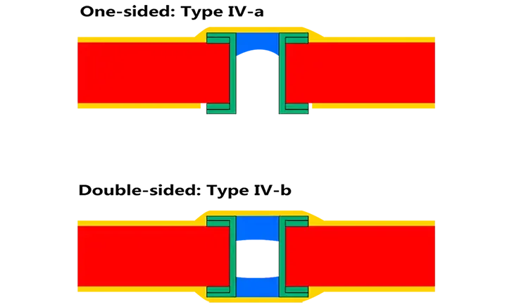
To mitigate the risk of cracks caused by encapsulated gas during the soldering of double-sided plugged vias on a multi-layer PCB, it is recommended to use the one-sided plugging method, specifically Type III-a or Type IV-a plugging techniques. These approaches entail plugging the vias on only one side of the board, thereby lowering the chances of encountering gas encapsulation issues.
Application
Efforts have been taken to optimize the manufacturing process through the integration of vacuum adaptation. In addition, measures have been implemented to prevent solder paste from inadvertently rising up to the component side, thereby ensuring effective protection during the manufacturing process.
Parameters
| Covering | Min Drill Diameter | Max Drill Diameter |
| Via Filling | 0.25mm | 0.5mm |
Designation
To ensure proper communication with the PCB manufacturer regarding vias that require filling, it is advisable to duplicate the vias onto an extra layer and explicitly label it in the fabrication notes. This will help ensure that the manufacturer is aware of the specific vias that require filling, thereby minimizing the likelihood of errors or misunderstandings during PCB production.
Via Filling
● IPC-4761 Type V (Filled Via): A conducting or non-conductive material poured into the via hole, completely filling it.
● IPC-4761 Type VI (Filled & Covered Via): An additional layer of dry film or liquid solder mask applied over the filled Type V via to mask it.
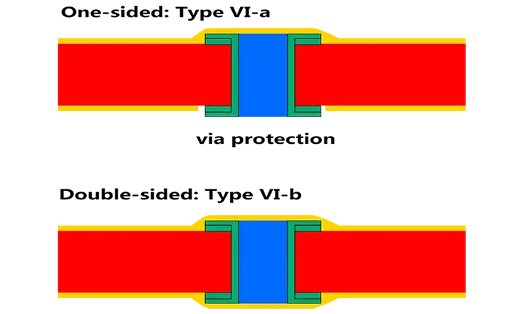
● IPC-4761 Type VII (Filled & Capped Via): An additional layer of dry film or liquid solder mask applied over the filled Type V via to mask it.
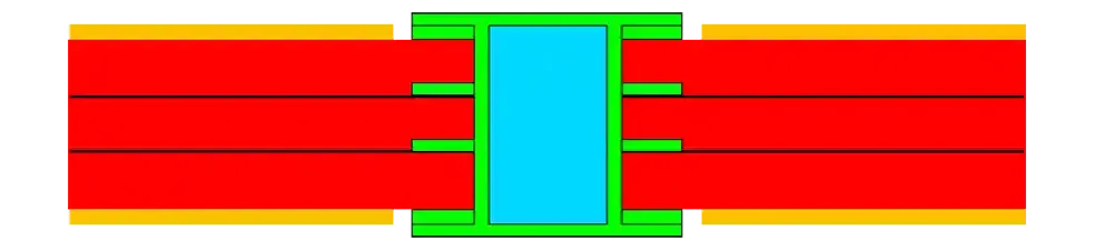
Via Filled and Capped Technology is a widely used solution for Via-in-Pad (VIP) requirements and is equally suitable for stacked and staggered via, as well as microvia in HDI (High-Density Interconnect) boards. One key advantage of via plugging is its facilitation of further routing of conductor traces between BGA vias. Moreover, the use of filled and capped vias is also a viable option for blind vias.
Application
Via filling and capping technology offers several advantages, including space-saving benefits and simplified implementation of Via-in-Pad Technology for components like BGAs. It also offers protection against errant solder paste that could float up to the component side and supports sequential build-up (SBU) multilayer stacking and staggered Microvia configurations.
Parameters
| Covering | Min Drill Dia. | >Pad Dia. | Max Drill Dia. | >Pad Dia. | Aspect Ratio |
Filled & Capped IPC-4761 Type VII | 0.15mm | 0.35mm | 0.4mm | 0.6mm | 1:12 |
Filled & Capped eletroplated | 0.1mm | 0.3mm | – | – | 1:10 |
NOTE: Filled and capped The aspect ratio of blind vias 1:1
Designation
To ensure accurate communication with the PCB manufacturer when requesting via plugging, it is recommended to create a duplicate of the vias that require filling on a separate layer and designate it accordingly. The layer should be appropriately labeled through the application of solder paste. This approach ensures that the manufacturer receives clear and precise instructions, thereby minimizing the risk of errors during production.
Application of Via Protection Techniques
The application of via protection techniques depends on the specific requirements of the PCB design. Some common applications include:
● RF circuits: RF circuits have specific requirements for via protection due to the high frequencies used in these applications. Specialized techniques such as “via-in-pad” or “blind via” can be used to reduce parasitic capacitances and inductances introduced by the vias.
● High-powered circuits: High-powered circuits generate a lot of heat, which can damage the vias and affect their electrical performance. To protect the vias in these applications, additional via-paste or copper filling is used, which helps to distribute the heat generated by the circuit more evenly.
● High-frequency circuits: In high-frequency circuits, via performance can impact overall signal integrity. Techniques such as “back-drilling” can be used to remove the via stub and reduce signal reflections.
● Circuit reliability: To improve overall circuit reliability, vias can be filled with materials such as resin or copper to provide additional mechanical support, reduce the risk of via cracking or damage during reflow process, or to prevent the ingress of contaminants.
By selecting the most suitable via protection technique based on specific requirements, users can ensure that they are achieving the best possible signal integrity and overall performance for their PCB design.
Future Developments and Trends in Via Protection
Current and future developments in via protection are focused on improving the reliability and performance of PCB designs. Some emerging trends include:
● New material advancements: Emerging materials such as polyimide or flexible circuit board materials present new challenges in via protection design. As such, new material sets are being explored and developed that can improve the performance of via protection techniques.
● Implementation of advanced manufacturing techniques: Laser drilling and plating techniques are being developed to create smaller and more precise vias, allowing for higher density designs. Additional improvements in additive manufacturing techniques, such as 3D printing, could lead to significantly higher precision and accuracy in via protection techniques.
● Improved ESD protection: As sensitive electronic components continue to become smaller and more densely packed on PCBs, the risks of ESD damage are increasing. New via protection techniques are being developed which offer better protection from ESD events.
● Design for high-frequency and high-speed signal integrity: As PCBs become denser and have higher frequencies, designers must address the challenges created by signal integrity. New design methodologies that account for both the electrical and mechanical aspects of via protection are being developed to meet these challenges.
By staying up-to-date with the latest developments and trends in via protection, designers can ensure that their PCB designs remain cutting-edge and reliable.
Summary
Filling and plugging vias can help enhance the reliability of a printed circuit board (PCB) by minimizing the risk of air or liquid becoming trapped within the vias. This improves assembly yields, ensuring the continuity of the final product. However, in our production processes, we prioritize the use of filled vias due to their superior benefits and advantages over plugged vias.
At JarnisTech, we have more than 20 years of experience in delivering PCBs across various industries. We offer a comprehensive range of circuit board types, from tented vias to filled and plugged holes, providing customized solutions to suit your requirements. Our commitment to delivering high-quality PCB manufacture and assembly services is paramount, and our team of professionals provides unparalleled after-sales service and maintenance support. In case of any queries, please feel free to contact us through our website.
We recommend that you select a suitable type of via protection based on your desired PCB quality and budget. If you require guidance on the best Via protection types for your board, please do not hesitate to contact us, and we will assist you accordingly.
Related Posts:
1. What Is PCB Etching and How to Make a perfect PCB Etching?
2. The Best PCB Panelization Guide
3. The Importance of 3D Printed PCBs in Modern Electronics Production
4. Understanding PCB Delamination: A Comprehensive Guide
5. The Best Backplane Printed Circuit Boards Factory
6. An Overview of Through-hole Technology (THT)
7. Detail Talk Surface Mount Technology
8. PCB Clone : Copy Your Printed Circuit Board
9. PCB Drilling: Definition, Technology Types and Process
10. Castellation PCB Fabrication: Castellated Hole (Plated Half Hole) Technologys Why So Important


