
Printed circuit boards (PCBs) continue to be at the core of most electronic devices, and their design involves a series of intricate processes. A vital characteristic of PCBs is the slot feature, which plays a pivotal role in electronics engineering.
Efficient PCB slot and cutout design enhances mechanical stability, thermal management, and electrical performance while ensuring compliance with industry standards like IPC-2221, IPC-6012, RoHS, REACH, and UL94. From CNC routing vs. laser cutting to signal integrity considerations, every aspect of slot and cutout placement affects fabrication tolerances, component soldering, and panelization. Avoiding common design mistakes and optimizing Gerber and drill file submissions streamlines production and reduces defects. Whether designing for RF circuits, high-power applications, or wearable devices, mastering these techniques ensures reliable performance and cost-effective manufacturing.
Understanding PCB Slots and PCB Cutouts
Designing PCB slots and cutouts might seem straightforward, but trust us, there’s more to it than just punching holes in a board. Whether you’re dealing with high-density PCB layouts, thermal dissipation strategies, or mechanical reinforcement, slots and cutouts have a direct impact on both electrical performance and structural integrity.
Engineers who overlook the details often end up with boards that warp under heat, suffer from poor signal integrity, or crack under mechanical stress—and nobody wants to deal with costly rework or field failures. In this section, we’ll break down the fundamentals, including key definitions, differences, and practical applications.
What Are PCB Slots and PCB Cutouts?
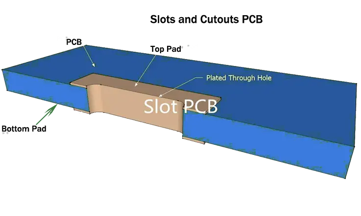
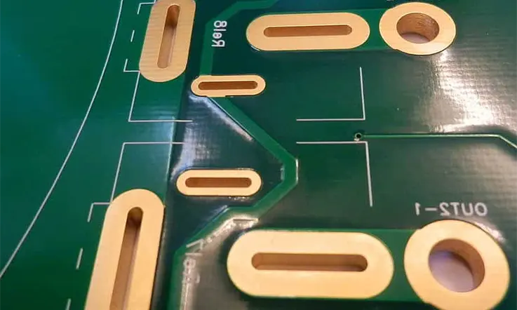
In PCB fabrication, slots and cutouts refer to non-circular openings machined into the board. These features vary in shape and size depending on design requirements, material constraints, and assembly needs. Unlike drilled holes, which are typically round, slots and cutouts accommodate rectangular, irregular, or custom-shaped components.
Manufacturing Methods for Slots and Cutouts-
1.Milling (CNC Routing):
●Most commonly used for fabricating non-plated slots and cutouts.
●Precision-controlled cutting ensures dimensional accuracy but increases fabrication time.
●Requires appropriate routing bits to prevent burn marks and fiber tearing in FR4 materials.
2.Laser Cutting:
●Used for high-precision PCBs, especially in RF and microwave applications.
●Provides a clean edge finish, reducing post-processing needs.
●Best suited for flexible and thin substrates, where mechanical stress must be minimized.
3.Punching and Stamping:
●Common in high-volume production where consistency is required.
●Suitable for standardized cutout shapes but may lead to burr formation if not carefully managed.
●Less precise than CNC milling but cost-effective for mass production.
4.EDM (Electrical Discharge Machining):
●Used for metal-core and exotic PCB materials.
●Allows for highly precise micro-cutouts in heat-sensitive boards.
●Each method has trade-offs in cost, speed, and precision, and the choice depends on material selection, production volume, and required tolerances.
The Influence of PCB Slots and Cutouts on Manufacturing and Assembly
Fabrication Constraints and Design Rules-
PCB manufacturers define specific guidelines for slots and cutouts to ensure smooth production:
●Minimum Slot Width: Typically ≥ 0.6mm, based on routing tool capabilities.
●Clearance from Copper Features: At least 0.5mm, preventing delamination risks.
●Edge-to-Edge Distance: Maintains mechanical stability and prevents warping.
Neglecting these factors can result in rough edges, copper peeling, or structural defects, leading to potential fabrication issues.
Impact on PCB Assembly and Soldering-
●Solder Mask Considerations: Improperly placed slots can lead to mask misalignment, exposing conductive areas unintentionally.
●Through-Hole Component Fitting: Slots designed for THT components need adequate space for lead bending and secure mounting.
●Thermal Expansion Effects: Cutouts must be arranged thoughtfully to avoid stress concentrations during reflow soldering.
Understanding these aspects early in the design process helps us avoid common pitfalls during manufacturing and assembly.
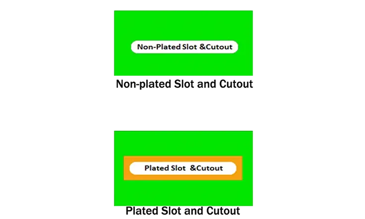
Plated vs. Non-Plated Slots: Differences and When to Use Each
How Plated and Non-Plated Slots Are Manufactured-
1.Plated Slots:
●Created by drilling oversized holes, followed by copper plating along the inner walls.
●Used for through-hole components requiring electrical continuity.
2.Non-Plated Slots:
●Routed after the copper plating process, leaving edges free of metal layers.
●Used for mechanical clearances, mounting points, and ventilation.
Quality Control in Slot Fabrication-
●Optical Inspection: Ensures dimensions meet specifications.
●X-Ray Analysis: Used for multilayer boards to verify slot positioning.
●Mechanical Stress Testing: Confirms that slot placement does not weaken PCB structure.
Mechanical and Electrical Considerations for PCB Slots and PCB Cutouts
When designing PCB slots and PCB cutouts, it’s not just about carving out space for components or improving airflow. These design elements impact mechanical stability, material integrity, and electrical performance. If not properly planned, slots and cutouts can lead to structural weaknesses, stress fractures, and grounding issues—all of which could turn a well-engineered board into a manufacturing headache.
Let’s explore three critical aspects: how slots and cutouts influence a PCB’s mechanical strength, strategies for preventing material defects, and best practices for ensuring solid grounding and electrical isolation.
How PCB Slots and PCB Cutouts Affect Mechanical Stability?
A PCB isn’t just a carrier for electrical components—it’s a structural part of an electronic device. Slots and cutouts introduce discontinuities in the board, altering its rigidity and overall durability. If not properly designed, they can weaken mounting areas, cause bending under load, or even create failure points during handling and assembly.
How Slots and Cutouts Influence PCB Strength-
| Factor | Impact on Mechanical Stability | Design Recommendation |
| Size and Shape | Larger slots reduce overall board strength | Keep slot dimensions within recommended limits |
| Placement | Slots near mounting holes can cause fractures | Avoid placing slots near stress points |
| Material Thickness | Thinner boards are more prone to flexing | Increase thickness in critical areas |
| Layer Stackup Design | Unbalanced layer structure increases warping potential | Ensure symmetrical copper distribution |
Best Practices for Slot Placement in High-Stress Areas-
●Keep slots away from mounting holes, screw locations, and high-torque areas to prevent stress fractures.
●If multiple cutouts are needed, distribute them evenly across the board to avoid creating weak bending points.
●Reinforce sections with additional copper layers or fiberglass stiffeners if large slots are necessary.
Even small design tweaks can make a huge difference in PCB durability—and that’s something worth paying attention to before manufacturing starts.
Preventing Cracking and Delamination Around PCB Cutouts
One of the biggest headaches in PCB manufacturing is when slots and cutouts lead to cracks, layer separation, or delamination. This often happens due to poor material selection, excessive mechanical stress, or improper routing techniques.
Common Causes of Cracks and Delamination-
| Cause | Effect on PCB Reliability | Preventive Action |
| High Mechanical Stress | Stress points can cause micro-fractures | Add reinforcement around cutouts |
| Sharp Corners in Cutouts | Sharp angles create stress concentration zones | Use rounded internal corners |
| Incorrect Routing Techniques | Excessive tool pressure can weaken the laminate | Optimize cutting speed and bit size |
| Thermal Expansion Issues | Uneven heating during soldering can cause peeling | Ensure balanced material expansion rates |
Strategies for Avoiding Material Defects-
●Avoid sharp corners in cutouts—use a minimum radius of 1mm to reduce stress concentration.
●Ensure smooth routing of slots by using appropriate cutting speeds and sharp tool bits to prevent rough edges.
●Consider pre-baking PCBs before assembly to remove excess moisture, reducing the risk of delamination during reflow soldering.
Nobody likes dealing with failed boards due to cracked laminates—taking these steps ensures PCBs stay intact from production to deployment.
Ensuring Proper Grounding and Electrical Isolation with PCB Slots
PCB slots and cutouts are more than just mechanical elements—they directly influence electrical behavior. Poor placement can mess with grounding, cause unwanted signal coupling, and lead to EMI troubles.
Electrical Effects of Slots and Cutouts-
| Electrical Concern | Impact on PCB Performance | Design Solution |
| Interrupted Ground Planes | Creates unwanted impedance shifts | Use ground bridges across slots |
| Increased EMI Susceptibility | Slots can form unintended antennas | Ensure continuous return paths |
| Signal Integrity Issues | Uneven trace impedance affects performance | Use stitching vias to control impedance |
| Dielectric Disruptions | Slots break the uniformity of insulating layers | Avoid slots near high-speed traces |
Techniques for Managing Grounding and Isolation in PCB Slot Design-
●If a slot breaks a ground plane, use stitching vias on both sides to maintain a low-impedance return path.
●Keep high-speed signal traces at least 20 mils away from slots to prevent unwanted coupling.
●When dealing with high-voltage isolation, make sure slots have adequate creepage and clearance distances as per IPC-2221 standards.
A well-thought-out slot placement strategy ensures that electrical performance remains stable—no one wants to debug signal noise issues after the board is already in production.
Design Guidelines for PCB Slots and PCB Cutouts in High-Performance PCBs
When working with high-performance PCBs, every structural detail can influence fabrication, assembly, and long-term durability. Slots and cutouts aren’t just about making space for connectors or improving heat dissipation—they interact with electrical performance, mechanical strength, and EMI shielding.
A well-thought-out approach ensures that manufacturing challenges are minimized, preventing last-minute design modifications that could delay production. Below, we’ll explore placement strategies, signal integrity considerations, and common pitfalls to keep your PCB layout tight and efficient.
Best Practices for Placing PCB Slots and PCB Cutouts in Your Layout
Placing slots and cutouts correctly can make all the difference between a smooth manufacturing process and a series of headaches that slow down production. Ignoring design rules can lead to board warpage, structural weaknesses, and alignment issues during assembly.
Guidelines for Effective Placement:
1.Maintain Structural Integrity-
●Avoid placing large cutouts or multiple slots too close to the board’s edge. This prevents the board from becoming too fragile, especially in rigid-flex designs.
●If a slot is necessary near the edge, reinforce it with a copper pour or additional routing clearance.
2.Ensure Proper Alignment for Components-
●Plated slots for through-hole components must align with fabrication tolerances, ensuring a snug fit.
●Non-plated slots should account for thermal expansion to avoid stress fractures during reflow soldering.
3.Consider Manufacturing Constraints-
●CNC routing and laser cutting have minimum width requirements—typically ≥0.6mm for mechanical stability.
●Routing tools wear over time, affecting cut precision—so keep slot tolerances within manufacturer recommendations.
If you’re working on complex layouts, collaborating with your PCB manufacturer (JarnisTech) early can prevent unexpected hiccups when your board hits the production line.
How PCB Slots and PCB Cutouts Impact Signal Integrity and EMI?
Slots and cutouts don’t just affect mechanical properties—they can also interfere with signal transmission, grounding efficiency, and electromagnetic interference (EMI). If not accounted for in the design phase, these issues can turn into board-level noise, crosstalk, or impedance mismatches that reduce circuit performance.
Electromagnetic Impact of Slots and Cutouts:
1.Interrupted Ground Planes Cause EMI Issues-
●A poorly placed slot in a ground plane can create unwanted radiation paths, leading to higher EMI emissions.
●Using stitching vias around a slot helps maintain signal return paths, reducing electromagnetic leakage.
2.Signal Integrity in High-Speed Designs-
●If a high-frequency trace crosses a slot or cutout, it can introduce reflections and signal loss.
●Keeping high-speed traces away from these features avoids transmission line disruptions.
3.Minimizing Noise in Sensitive Circuits-
●Analog and RF circuits should have dedicated, uninterrupted ground planes, ensuring minimal interference.
●Isolated power domains can benefit from strategically placed cutouts, but they should be modeled for impedance variations.
Avoiding Common Mistakes in PCB Slot and PCB Cutout Design
It’s easy to overlook slot and cutout design details, but some mistakes can lead to costly redesigns or outright manufacturing failures. Many of these issues stem from misalignment, improper sizing, or ignoring material limitations.
Top Design Errors and How to Avoid Them:
1.Misaligned Slots in Plated Through-Holes-
●If plated slots are misaligned with drill and routing layers, they can create poor solder joints or weak electrical connections.
●Double-check Gerber and NC drill files before sending them for fabrication.
2.Cutouts Too Close to Copper Traces-
●Placing a cutout too close to a trace can lead to delamination or peeling during assembly.
●Keep at least 0.5mm clearance between cutouts and copper features to avoid manufacturing defects.
3.Uneven Stress Distribution-
●Irregular slot shapes can create stress concentration points, causing micro-cracks over time.
●Rounded corners in slots reduce stress buildup, improving mechanical reliability.
Manufacturing PCB slots and cutouts requires attention to detail, and even small adjustments can make the difference between a flawless board and one that needs costly rework. If you’re tackling a new layout, triple-checking DFM (Design for Manufacturability) guidelines can keep things on track.
H2: How to Use Eagle Software to Design PCB Slot and Cutouts?
If you’re working with Eagle for PCB design, you might be wondering if the software supports creating slots. Slotted holes are widely used in PCBs, especially for components that need to handle rising current efficiently. Components with wider pins tend to offer better mechanical stability, making them a go-to choice in many designs.
To lay out PCB slots and cutouts, you’ll need to work with a through-hole pad that has a diameter matching the intended slot width. An oval-shaped pad usually does the trick.
When drawing slotted holes and cutouts, there are multiple approaches, including the use of the dimension layer. However, this method has some quirks—autorouting might not properly recognize the inside of the pad, leading to dimension errors. To keep things precise, always ensure that the drill size of the pad stays within the PCB slot’s outline.
Once the design checks out, the next move is sending the Gerber file to the PCB manufacturer, along with a note specifying that the designated slots need to be milled out. This step is what seals the deal, making sure the finished board looks and functions exactly as intended.
Manufacturing Techniques for High-Precision PCB Slots and PCB Cutouts
Designing PCB slots and cutouts is not just about making room for connectors or mechanical supports—it’s about ensuring they are produced with accuracy and repeatability. Different manufacturing methods impact slot geometry, surface quality, and board durability. Therefore, if you’re working with standard FR4, high-frequency laminates, or flexible PCBs, selecting the right fabrication approach can make or break the final board’s performance.
Let’s explore how CNC routing and laser cutting compare, how slot dimensions affect production tolerances, and what edge finishing methods can improve board quality.
CNC Routing vs. Laser Cutting: The Best Methods for PCB Slots and PCB Cutouts
When it comes to fabricating PCB slots and cutouts, two of the most commonly used methods are CNC routing and laser cutting. Each has its place in PCB manufacturing, depending on board thickness, slot shape, and volume requirements.
Comparison of CNC Routing and Laser Cutting for PCB Slot and Cutout Manufacturing-
| Feature | CNC Routing | Laser Cutting |
| Best suited for | Standard FR4, plated slots, large cutouts | Thin PCBs, complex geometries, RF circuits |
| Minimum slot width | 0.6mm (depends on router bit size) | 0.1mm (higher precision for fine details) |
| Edge characteristics | Slightly rough, requires post-processing | Smooth but may have thermal effects |
| Production speed | Moderate | Faster for intricate designs |
| Mechanical stress | Applies slight stress during machining | No direct mechanical force |
| Plating capability | Ideal for plated slots | Not suitable for plated slots |
| Cost efficiency | Lower for large-scale production | More cost-effective for small-batch or fine-detail work |
Key Considerations-
●CNC routing handles plated slots well, making it the go-to option for connector pins and mounting points.
●Laser cutting provides finer detail, making it useful for RF circuits and microelectronics, but it may cause thermal discoloration on some materials.
●For thin substrates or intricate cutouts, laser cutting offers better accuracy, but for high-volume runs, CNC routing is often more practical.
How PCB Slot and PCB Cutout Size Affects Fabrication Tolerances?
Even small deviations in slot and cutout dimensions can lead to component misalignment, mechanical instability, or assembly issues. We must follow specific tolerance standards to maintain consistent results across production batches.
Recommended Fabrication Tolerances for PCB Slots and Cutouts-
| Feature | CNC Routing Tolerance | Laser Cutting Tolerance |
| Slot Width | ±0.1mm – ±0.2mm | ±0.05mm – ±0.1mm |
| Slot Length | ±0.2mm – ±0.3mm | ±0.1mm – ±0.2mm |
| Plated Slot Diameter | ±0.05mm – ±0.1mm | Not applicable |
| Edge Roughness | Medium (Deburring needed) | Smooth (Minor thermal effect) |
Practical Insights-
●Tighter tolerances require more precise tooling, which may affect production costs.
●Plated slots must account for additional copper thickness, ensuring a snug fit for press-fit connectors or screw terminals.
●Longer slots may require reinforcement, particularly in high-vibration environments.
Designing within realistic fabrication limits can help prevent unexpected yield issues and unwanted redesigns down the road.
Ensuring High-Quality Edge Finishing for PCB Slots and PCB Cutouts
Edge finishing isn’t just about looks—it affects how components fit, how well slots align with plated features, and even long-term board reliability. Poorly finished edges can lead to burrs, micro-fractures, or uneven copper deposition.
Edge Finishing Methods for PCB Slots and Cutouts-
| Edge Finishing Method | Commonly Used For | Benefits |
| Mechanical Deburring | CNC-routed slots | Removes sharp edges, improves handling |
| Plasma Treatment | Laser-cut edges | Eliminates thermal residues, improves adhesion |
| Vibratory Tumbling | CNC-routed PCBs | Smooths edges in high-volume production |
| Chemical Edge Smoothing | RF and high-frequency boards | Reduces material loss, maintains slot accuracy |
Best Practices for Edge Finishing-
●If using CNC routing, post-processing like deburring or vibratory tumbling helps achieve cleaner slot edges.
●For laser-cut boards, plasma treatment removes carbonization, making the slots suitable for soldering or press-fit components.
●When working with plated slots, ensuring the edges remain smooth helps maintain consistent copper deposition.
If connectors, shields, or mounting hardware are involved, edge quality is worth the extra attention. Nobody wants a board that doesn’t fit right when it gets to assembly!
How to Avoid Manufacturing Defects in PCB Slot and PCB Cutout Design?
Designing PCB slots and PCB cutouts may seem straightforward, but small missteps can lead to fabrication headaches. When dimensions, copper clearances, or drill files aren’t set up correctly, we either struggle to produce the board as intended or send it back for revisions. That means delays, extra costs, and a whole lot of frustration.
By paying close attention to copper clearances, cutout dimensions, and proper file submissions, you can dodge these issues before they become full-blown problems. Let’s go over the common trouble spots and the best ways to handle them.
Preventing Copper Clearance Issues in Plated PCB Slots
Plated PCB slots are used for edge connectors, mounting points, and specialized components. Since these slots are drilled and then plated with copper, proper clearance must be maintained to prevent electrical shorts, uneven plating, or weak structural integrity.
One of the most common issues occurs when copper pours or traces are placed too close to the slot edge. This can result in poor plating adhesion or even a breakdown of insulation between different circuit layers. If we has to manually adjust the clearance, it can slow down production or cause unexpected electrical behavior.
How to Get Copper Clearances Right-
●Stick to manufacturer guidelines—most fabrication houses recommend at least 0.2mm clearance between copper and plated slots.
●Check for overlapping traces—high-speed signals running too close to plated slots can experience interference.
●Use DRC (Design Rule Check) settings in your PCB software to flag clearance violations before submission.
When these factors are addressed early in the design process, manufacturing moves forward without unnecessary back-and-forth adjustments.
Common Causes of PCB Failures Due to Incorrect PCB Cutout Dimensions
Poorly designed PCB cutouts can lead to misalignment, mechanical stress, and soldering problems. A cutout that’s too small for a component forces assembly teams to make manual adjustments, while oversized cutouts can weaken the board’s structure.
Some issues show up only after production begins. For example, if a cutout is placed too close to a high-current trace, thermal expansion during operation may cause cracks, leading to unexpected failures.
How to Avoid Dimensional Mistakes in PCB Cutouts-
●Double-check component datasheets before finalizing cutout sizes. A small mismatch can mean a big problem.
●Maintain safe spacing from high-stress areas, such as mounting points or high-power traces.
●Use precise routing techniques to avoid rough edges that could lead to stress fractures.
By fine-tuning these aspects, your board will hold up during both assembly and real-world use.
PCB Slot and PCB Cutout Considerations in PCB Assembly and Panelization
Designing PCB slots and cutouts isn’t just about mechanical fit—what happens during assembly and panelization can make or break the entire process. So, whether it’s soldering challenges, stress points, or panel breakout strategies, every choice affects fabrication yield and long-term reliability.
Let’s break it down into three major considerations: how slots and cutouts impact soldering and placement, how to minimize board warpage, and how to optimize panel breakout methods.
How PCB Slots and PCB Cutouts Affect Soldering and Component Placement?
It’s easy to overlook, but slots and cutouts can create unexpected headaches during PCB assembly. They impact thermal distribution, influence solder paste application, and can even cause misalignment issues if not properly accounted for.
Challenges When Soldering Near PCB Slots and Cutouts-
| Issue | Impact on Assembly | Solution |
| Uneven Heat Distribution | Can lead to cold solder joints or tombstoning | Use thermal relief pads near slot edges |
| Stencil Printing Issues | Openings near cutouts may cause paste bleeding | Adjust stencil design to control paste flow |
| Pick-and-Place Misalignment | Components near cutouts may shift during reflow | Ensure fiducial marks are placed strategically |
| PCB Panel Strength Reduction | Large cutouts can make panels fragile during handling | Use breakaway tabs to reinforce structure |
Best Practices for Soldering Near PCB Slots and Cutouts-
●If a slot is too close to an SMT pad, the reflow oven may heat unevenly, leading to cold joints.
●Pick-and-place machines rely on a stable surface—avoid placing components directly next to large slots, as they can sink slightly during placement.
●To prevent warping in reflow, distribute slots symmetrically whenever possible.
Preventing PCB Warpage and Stress Concentration Around PCB Cutouts
Slots and cutouts change how stress moves through a PCB panel, and if not properly planned, they can turn your board into a banana-shaped headache. Warping affects pick-and-place alignment, reflow consistency, and even long-term durability.
Why Do PCBs Warp When Using Slots and Cutouts?
1.Uneven Copper Distribution – If one side of the board has more copper weight, it contracts differently than the other side when cooling.
2.Panelization Weak Spots – Large cutouts create natural bending points, especially when paired with V-scoring or routing.
3.Reflow Oven Heat Cycling – If slots and cutouts are poorly placed, localized stress can twist the board after cooling.
Design Adjustments to Minimize PCB Warping-
| Design Factor | How It Affects Warping | Solution |
| Slot and Cutout Symmetry | Asymmetrical layouts cause uneven stress | Keep cutout distribution balanced |
| Copper Distribution | Heavy copper on one side pulls during cooling | Use copper balancing techniques |
| Panel Reinforcement | Large cutouts weaken PCB rigidity | Add supporting rails or temporary tabs |
| Layer Stackup Adjustments | Uneven dielectric layers lead to warping | Ensure symmetrical layer stackup |
Pro Tips for Reducing Warpage-
●Never place large slots on only one side of the board—it’s like putting all the weight on one end of a seesaw.
●If the board requires breakaway tabs, ensure they are evenly distributed to avoid twisting.
●For multilayer PCBs, balance the copper layout on each layer—don’t leave one side heavily plated while the other is empty.
If your PCB starts looking like a potato chip after assembly, chances are cutouts and panel design need another look.
Using V-Scoring, Routing, and Breakaway Tabs for PCB Slot Optimization
When PCB slots and cutouts are part of a panelized design, removing individual boards cleanly is just as important as their placement. The wrong breakout method can leave rough edges, excessive stress, or even broken traces.
Common PCB Panelization Methods for Slots and Cutouts-
| Method | How It Works | Best Used For |
| V-Scoring | Boards are partially cut with a V-shaped groove, then snapped apart | Straight-line slots and cutouts |
| Routing | A router bit cuts through the board outline, leaving small connecting tabs | Curved slots, irregular cutouts |
| Breakaway Tabs | Small tabs with drilled perforations hold the PCB in place | Boards with large cutouts |
Which One Works Best for PCB Slots?
●V-scoring is fast and clean, but only works for linear slots.
●Routing allows curved slots, but generates fiberglass dust during depaneling.
●Breakaway tabs work well, but need careful placement to avoid stress near cutouts.
Best Practices for Panelization with Slots and Cutouts-
●Always reinforce large cutouts with temporary support rails in panelized designs.
●If using breakaway tabs, keep them away from delicate copper traces to prevent damage when snapping boards apart.
●If using routing, check with your manufacturer about tool diameter limitations—some slots may be too thin for standard router bits.
Carefully planning panel breakout methods helps prevent edge defects and ensures boards separate cleanly without damaging traces.
Advanced Applications of PCB Slots and PCB Cutouts in Electronics
Modern electronics are pushing design boundaries, requiring PCB slots and PCB cutouts to go beyond simple mechanical functions. Whether it’s managing heat in power electronics, optimizing RF performance, or enabling compact wearable devices, these structural features are playing an increasing role in specialized applications.
For designers working with high-power, high-frequency, or flexible circuit designs, integrating PCB slots and PCB cutouts effectively can mean the difference between a product that meets specifications and one that struggles in real-world use. Let’s break down how these features contribute to thermal management, RF performance, and next-gen flex PCBs.
Using PCB Slots and PCB Cutouts for Thermal Management and Heat Dissipation
Heat dissipation is one of the biggest challenges in power electronics, LED drivers, and high-performance computing. While thermal vias and heatsinks handle most of the workload, PCB slots and PCB cutouts can improve airflow, reduce localized heat buildup, and provide space for active cooling components.
How PCB Slots Help with Heat Management-
●Enhancing convection cooling – Strategically placed PCB slots allow natural or forced air to pass through, improving heat dissipation.
●Reducing thermal stress – Cutouts around heat-generating components can prevent heat from spreading to sensitive areas of the board.
●Providing space for heatsinks – Some power circuits require heatsinks mounted directly onto the PCB. Cutouts ensure a perfect fit while preventing electrical contact with traces.
Design Considerations for Thermal PCB Slots-
●Keep slots at least 0.5mm away from high-current traces to prevent mechanical weakening.
●Ensure plated edges are properly finished if slots are used near power components to prevent electrical shorts.
●Use staggered slots instead of a single large cutout to maintain PCB rigidity.
When used correctly, PCB slots and PCB cutouts don’t just shape the board—they actively contribute to temperature control and long-term reliability.
The Role of PCB Slots and PCB Cutouts in RF and High-Frequency PCBs
RF circuits and high-frequency PCBs require careful layout to maintain signal integrity and minimize electromagnetic interference (EMI). PCB slots and PCB cutouts are often used to separate different circuit regions, block unwanted coupling, and reduce parasitic capacitance.
Why RF Designs Rely on PCB Cutouts-
●Minimizing unwanted coupling – Slots between high-frequency traces help prevent crosstalk and improve signal integrity.
●Ground plane separation – PCB cutouts can isolate sections of a ground plane to create distinct RF paths.
●Reducing edge effects – Cutouts in RF shields prevent unwanted reflections that can distort signals.
Best Practices for RF PCB Cutouts-
●Place slots perpendicular to signal paths to minimize unwanted radiation.
●Avoid abrupt edges—smooth transitions prevent sudden impedance mismatches.
●Use grounded slots when needed—plated slots can act as barriers to contain EMI.
Flexible and Rigid-Flex PCB Slot Innovations for Wearable Devices
Wearable technology demands compact, lightweight, and mechanically flexible PCB designs. PCB slots and PCB cutouts in flexible and rigid-flex PCBs allow for increased flexibility, improved strain relief, and optimized sensor integration.
Why Wearable PCBs Use Slots and Cutouts-
●Improved bending capability – Strategically placed slots prevent material stress when the PCB flexes.
●Sensor integration – Cutouts provide openings for optical, pressure, and biometric sensors.
●Reducing mechanical failure – Eliminating rigid connections in flex regions prevents stress fractures.
Optimizing Slot Design for Wearable Devices-
●Use rounded edges instead of sharp corners to avoid stress concentrations.
●Reinforce slot edges with coverlay to protect traces near cutout regions.
●Keep slot width within manufacturer-recommended limits to maintain structural integrity.
Compliance and Industry Standards for PCB Slots and PCB Cutouts
Designing PCB slots and PCB cutouts isn’t just about getting the layout right—it also involves ensuring the board meets industry regulations. Whether it’s mechanical strength, material selection, or environmental compliance, ignoring established standards can lead to fabrication roadblocks, regulatory setbacks, and even product failures.
From the widely recognized IPC-2221 and IPC-6012 standards to international compliance requirements like RoHS, REACH, and UL certification, staying aligned with these regulations helps us avoid production delays and costly revisions. Let’s break down the most relevant guidelines and how they apply to PCB slot and PCB cutout design.
IPC-2221 and IPC-6012 Standards for PCB Slot and PCB Cutout Design
The IPC (Institute for Printed Circuits) standards serve as the foundation for PCB design and manufacturing across industries. When it comes to PCB slots and PCB cutouts, two main documents—IPC-2221 and IPC-6012—outline the recommended design practices and acceptance criteria.
What IPC-2221 Covers-
IPC-2221 acts as the universal PCB design standard, addressing general requirements for mechanical features like slots and cutouts. Key considerations include:
●Minimum spacing between slots and conductive elements to prevent short circuits.
●Slot width tolerances based on fabrication capabilities.
●Recommendations for plated vs. non-plated slots based on current-carrying needs.
How IPC-6012 Defines Quality Levels-
IPC-6012 focuses on performance and reliability, classifying boards into three levels:
●Class 1: Consumer-grade electronics with minimal reliability requirements.
●Class 2: Industrial and automotive-grade PCBs where long-term functionality matters.
●Class 3: High-reliability applications like aerospace and medical devices, where every detail in slot and cutout fabrication must meet tight tolerances.
Avoiding Common Pitfalls in IPC Compliance-
●Failing to meet minimum slot width requirements can lead to fabrication defects and rejected boards.
●Non-plated slots used incorrectly can weaken mechanical stability in connector areas.
●Ignoring slot-to-copper clearances may result in electrical shorts during assembly.
Before sending Gerber files to a manufacturer, ensure your slot and cutout dimensions align with IPC specifications—it’s a simple step that can prevent costly revisions down the road.
Ensuring RoHS, REACH, and UL Compliance for PCB Slots and PCB Cutouts
Beyond design guidelines, environmental and safety regulations shape how PCBs are manufactured, particularly when dealing with PCB slots and PCB cutouts that expose inner layers or require special material considerations.
RoHS and REACH: Keeping Hazardous Materials Out-
●RoHS (Restriction of Hazardous Substances): Ensures that materials used in PCB fabrication—including exposed areas around cutouts—are free from harmful substances like lead, mercury, and cadmium.
●REACH (Registration, Evaluation, Authorization, and Restriction of Chemicals): Addresses the use of chemicals in PCB manufacturing, particularly in plating processes for plated slots and cutouts.
UL Certification: Fire Safety for PCB Slots and Cutouts-
If a PCB is expected to handle high power or operate in safety-critical environments, UL (Underwriters Laboratories) certification is often required. UL 94 is the most relevant standard for PCB flammability, which applies to:
●Slot and cutout edges that expose inner laminate materials.
●Cutout areas near high-temperature components, which may need UL-approved flame-retardant materials.
●Plated slots in power circuits, where insufficient plating thickness can create heat buildup and potential safety risks.
Best Practices for Compliance-
●Confirm that PCB materials meet UL 94V-0 flammability ratings, especially around cutout edges.
●Work with certified manufacturers to avoid non-compliant board materials.
●Use proper plating thickness on conductive slots to meet safety and durability requirements.
With global electronics regulations tightening, ensuring compliance from the start saves time, cost, and legal headaches during mass production.
FAQs About PCB Slots and Cutouts
1.Do PCB cutouts affect thermal expansion and contraction?
Yes, cutouts can lead to uneven thermal distribution, potentially causing warpage or mechanical stress if not properly considered.
2.How do PCB slots impact the PCB panelization process?
Slots can weaken breakaway tabs and affect V-scoring efficiency, requiring adjustments in panel design for better stability.
3.What is the difference between oval and rectangular PCB slots?
Oval slots are smoother and easier to manufacture, while rectangular slots with sharp corners may require laser cutting or additional milling.
4.Are there any restrictions on the placement of PCB slots near traces?
Yes, placing slots too close to traces can cause copper peeling, signal interference, or mechanical weakness in the board.
5.Can PCB slots and cutouts improve high-voltage isolation?
Yes, slots are commonly used in high-voltage designs to increase creepage and clearance distances, reducing the risk of electrical arcing.
6.What file format should be used to define PCB slots for manufacturers?
Slots should be clearly specified in Gerber X2, ODB++, or separate mechanical layers in the CAD file to avoid fabrication errors.
7.Can PCB slots be used for weight reduction in large boards?
Yes, strategic slot placement can reduce overall PCB weight, which is useful for aerospace, automotive, and wearable electronics applications.
Related Posts:
1. What Is PCB Etching and How to Make a perfect PCB Etching?
2. The Best PCB Panelization Guide
3. The Importance of 3D Printed PCBs in Modern Electronics Production
4. Understanding PCB Delamination: A Comprehensive Guide
5. The Best Backplane Printed Circuit Boards Factory
6. An Overview of Through-hole Technology (THT)
7. Detail Talk Surface Mount Technology
8. PCB Clone : Copy Your Printed Circuit Board
9. PCB Drilling: Definition, Technology Types and Process
10. Castellation PCB Fabrication: Castellated Hole (Plated Half Hole) Technologys Why So Important


