
The management of thermal loads is a primary determinant of performance and longevity in power electronics. Hybrid Aluminum Printed Circuit Boards (PCBs) are a purpose-built construction for this challenge, providing an engineered framework for high-demand applications. This comprehensive guide covers the entire lifecycle of these specialized boards, from material science and precision fabrication to full turnkey assembly and advanced design considerations.
Defining Hybrid Aluminum PCBs: The Convergence of Power and Thermal Control
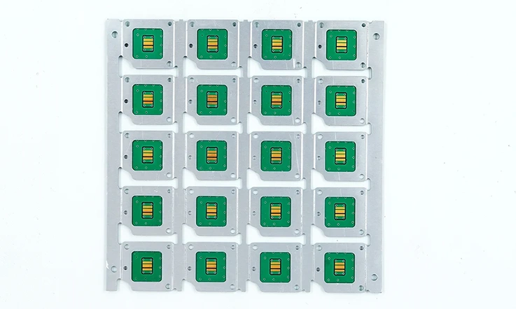
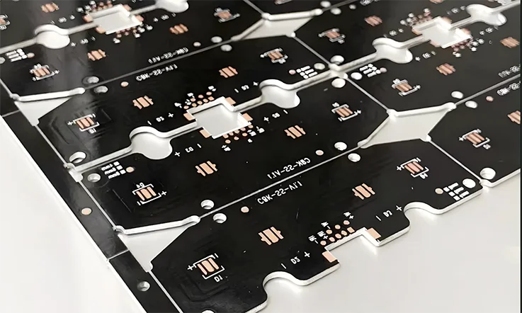
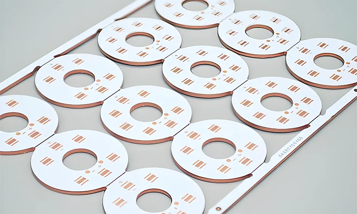
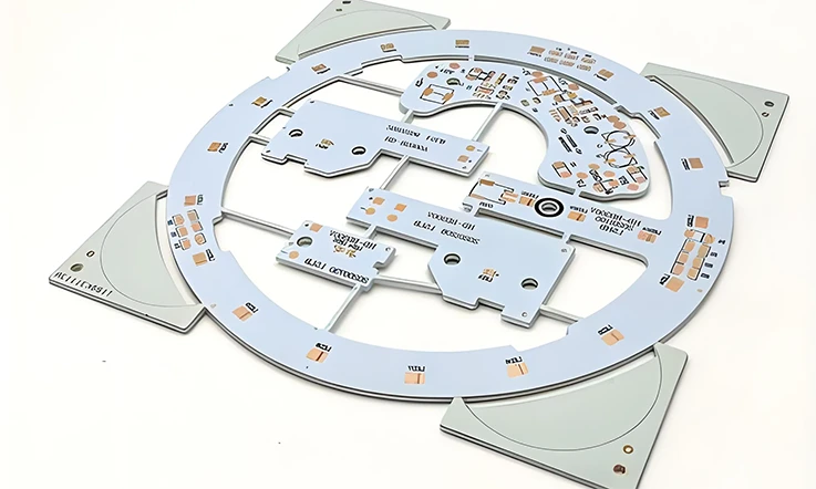
Hybrid Aluminum PCBs are engineered composite constructions intended for applications that generate substantial thermal energy. They are designed to manage significant heat while upholding electrical integrity under high-stress operating conditions. By combining multi-layered constructions with refined copper circuitry and a metal substrate, these boards provide a robust foundation for power electronic assemblies, ensuring predictable performance from the component to the system level, particularly in applications like LED modules, automotive power electronics, and advanced communication infrastructure that generate substantial thermal energy.
Anatomy of a Hybrid PCB: A Layer-by-Layer Breakdown
The architecture of a Hybrid Aluminum PCB employs a multi-layered structure engineered for high-current and thermally intensive designs. The construction is planned to preserve electrical integrity and optimize thermal dissipation throughout all operational phases. The fabrication process focuses on a precise stack-up built for performance and manufacturability.
●Aluminum Substrate: Provides a rigid mechanical foundation and an efficient thermal pathway to dissipate heat away from active components.
●Dielectric Layers: Utilizes materials with low thermal resistance to facilitate effective heat transfer while ensuring complete electrical isolation between conductive layers.
●Copper Circuits: Engineered with precise trace geometries and thicknesses to manage high currents and minimize thermal buildup.
●Thermal Vias: Strategically positioned directly under power components, creating a direct conduit for heat to flow toward the aluminum base, effectively lowering component temperatures during operation.
Performance Advantages in Demanding Electronics
For projects involving LED arrays, motor drives, and RF communication modules, designs must withstand repetitive thermal cycles and electrical stress without degradation. The use of Hybrid Aluminum PCBs delivers a specific set of performance characteristics.
Superior Thermal Regulation
The construction of these boards provides a highly efficient method for heat dissipation. This property is intrinsic to the board’s structure.
●The integrated aluminum substrate and thermal vias ensure effective heat transfer away from components like LEDs and MOSFETs. This lowers their operating temperatures during prolonged use and enables stable device operation.
Compact and Dense Layouts
Effective inherent thermal management allows for greater design freedom and miniaturization, enabling competitive product design in modern electronics.
●The reliance on bulky external heatsinks is reduced or eliminated. This allows for the design of smaller product footprints and denser component arrangements, a specific advantage in applications such as modern LED lighting and RF power circuits where space is at a premium.
Enhanced Mechanical Soundness
The physical stability of a PCB affects its operational life, especially in environments subject to vibration or physical shock. The metal core provides a level of robustness that standard laminates cannot offer.
●The rigid aluminum core minimizes board flexure during manufacturing and under operational stress. This physical stability safeguards solder joints and delicate components from damage caused by vibration and physical impacts, a frequent requirement in automotive and industrial settings.
Expanded Design Freedom
The materials of construction for Hybrid Aluminum PCBs offer a range of engineering options to precisely match application requirements.
●Copper weights and dielectric materials can be tailored to meet specific power and frequency requirements. This empowers engineers to optimize device performance while maintaining practical assembly workflows. For builders of LED lighting drivers, 5G modules, and energy systems, these boards facilitate dependable operational results across volume fabrication runs and help achieve compact, high-efficiency designs.
A Comparative Analysis: Aluminum PCBs vs. Alternative Thermal Solutions
Engineers facing thermal management challenges evaluate several options. An understanding of where Hybrid Aluminum PCBs fit within this landscape allows for an informed decision. The following comparison details the trade-offs in performance, cost, and reliability against two common alternatives.
Scenario 1: Hybrid Aluminum PCB vs. Standard FR-4 with an Attached Heatsink
This comparison addresses an integrated thermal solution against a conventional, multi-part assembly. It is a frequent decision point for designers moving into higher power densities.
Thermal Efficiency:
The Hybrid Aluminum PCB offers a significantly lower overall thermal resistance. Heat from a component must travel through the solder, the copper pad, a thin, high-conductivity dielectric, and directly into the aluminum heat spreader. In the FR-4 solution, heat faces a thermal bottleneck as it travels through the full thickness of the thermally-insulative FR-4 laminate (~0.1-0.2 W/mK), a thermal interface material (TIM), and finally to the heatsink. The FR-4 itself presents a high thermal resistance, resulting in higher component operating temperatures compared to the direct path offered by an aluminum PCB.
Data Table: Thermal Performance Comparison:
| Metric | Hybrid Aluminum PCB | FR-4 + Heatsink |
| Thermal Conductivity (Dielectric) | 1–5 W/mK | 0.1–0.2 W/mK |
| Typical Thermal Resistance | Lower | Higher |
| Component Operating Temperature | Lower (at equivalent power levels) | Higher |
| Heat Path Complexity | Simple, direct | Multiple interfaces, complex |
System Reliability & Simplicity:
The monolithic structure of an aluminum PCB is inherently more reliable. The FR-4/heatsink assembly involves multiple components (PCB, TIM, heatsink, mounting hardware). This introduces multiple points of potential failure. The TIM can degrade over time through “pump-out” from thermal cycling, and mechanical fasteners can loosen under vibration, both leading to a substantial increase in thermal resistance. The integrated nature of the aluminum PCB removes these failure modes.
Total Cost of Ownership (TCO):
While the unit cost of an aluminum PCB may be higher than a bare FR-4 board, the total cost of ownership is often lower. The FR-4 solution requires additional procurement, inventory management, and assembly steps to attach the heatsink. These costs of labor and logistics are absent with the integrated aluminum board, streamlining the manufacturing process.
Physical Profile and Weight:
The integrated aluminum solution is invariably thinner, lighter, and more compact. It removes the bulk of the external heatsink and mounting hardware, enabling sleeker product designs, a tangible advantage in space-constrained applications.
Scenario 2: Hybrid Aluminum PCB vs. Ceramic Substrates (e.g., Alumina, AlN)
This comparison addresses the high-end of the thermal management spectrum. It reveals that for many applications, ceramics represent a costly level of engineering that may not be necessary.
Performance-to-Cost Ratio:
This is a primary differentiator. High-performance ceramics like Aluminum Nitride (AlN) offer exceptional thermal conductivity. However, the overall system performance also depends on the circuit layer. For many applications, the performance of a well-designed Hybrid Aluminum PCB with a thin, advanced dielectric is sufficient and approaches that of lower-grade ceramics like Alumina (Al2O3) at a fraction of the cost.
Data Table: Performance and Cost:
| Metric | Hybrid Aluminum PCB | Ceramic Substrates (Alumina, AlN) |
| Thermal Conductivity | 1–5 W/mK (dielectric) | Alumina: ~20–30 W/mK, AlN: ~170–200 W/mK |
| Relative Cost | Lower | Higher |
| Thermal Performance | Adequate for many applications | Superior, often beyond requirements |
Mechanical Durability and Manufacturability:
Aluminum is a ductile, robust metal. It is easy to machine, can withstand significant mechanical shock and vibration, and can be fabricated in large panel sizes. Ceramics, by contrast, are brittle. They are prone to chipping or cracking if dropped or subjected to mechanical stress and are more challenging and costly to machine into complex shapes or drill with fine features.
Design Flexibility:
Aluminum PCBs offer the design flexibility of traditional PCB design, including multi-layer constructions with internal power and ground planes. While multi-layer ceramic technologies exist (e.g., HTCC, LTCC), they involve more complex and restrictive design rules and processing, limiting the freedom available to circuit designers. The aluminum platform provides a more versatile and familiar design environment.
Key Industries and High-Performance Applications
Hybrid Aluminum PCBs address the needs of several industries that require robust thermal handling paired with precise electrical performance. Their adoption is driven by the need for reliability under strenuous operating conditions.
Automotive and EV Power Electronics
In the automotive sector, reliability is a baseline expectation. These boards are found in applications where both thermal and mechanical stress are constant factors.
●In electric drive control units and LED headlamp assemblies, these boards reduce the surface temperatures of heat-sensitive integrated circuits. This allows for sustained functionality under continuous drive conditions. The aluminum-backed structure also mitigates the effects of mechanical vibration.
Application Example: A 22kW Electric Vehicle Onboard Charger (OBC) utilizes a 4-layer aluminum PCB with 3oz copper planes. This construction effectively manages the thermal load from its SiC MOSFETs during peak charging cycles. The design maintains semiconductor junction temperatures below the 125°C operational ceiling, a performance metric unachievable with a standard FR-4 assembly of the same physical volume, which would otherwise exceed 150°C and trigger thermal throttling.
5G and Communication Modules
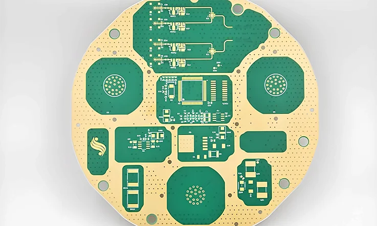
High-frequency applications generate concentrated heat that can directly impact signal integrity. Managing this heat at the source is a prerequisite for performance.
●For high-frequency power amplifiers, these boards manage heat directly at the source, beneath RF transistors and power stages. This approach lessens thermal gradients that can affect signal behavior. Copper stack-ups are configured for controlled impedance routing while leveraging thermal vias for localized heat management.
Application Example: A Doherty power amplifier for a 5G macro base station is built on a hybrid aluminum PCB. The board features controlled impedance traces for the RF paths and a dense array of thermal vias directly under the GaN transistors. This configuration prevents thermally-induced phase shifts and maintains signal linearity, ensuring the amplifier meets stringent 3GPP performance standards across all operating temperatures.
Renewable Energy and Industrial Automation
In energy and automation, systems are expected to operate continuously for years, often in harsh environments. Long-term thermal stability is therefore a primary design requirement.
●In solar inverter control boards and wind system power stages, these boards are subjected to sustained heat from power devices operating at high currents. By providing effective thermal paths, the PCBs support continuous operation in demanding outdoor or enclosed environments. These applications leverage aluminum-backed PCB assemblies to maintain operational benchmarks, enabling our engineers to focus on optimizing device efficiency and meeting size constraints.
Application Example: An industrial motor drive rated for 50kW continuous output employs a 2.0mm thick aluminum substrate PCB to cool its IGBT power modules. The board’s mechanical rigidity and efficient heat dissipation prevent solder joint fatigue failures that would otherwise occur from the daily thermal cycling experienced in a factory environment, thus extending the operational lifetime of the drive system.
The Manufacturing Blueprint: Material Science and Fabrication
The construction of Hybrid Aluminum PCBs involves a precise integration of materials within engineered stack-up designs. The objective is to manage heat effectively while preserving the fidelity of electrical pathways, forming the structure that power devices and high-brightness LED modules require.
A Deep Dive into Material Science and Stack-up Construction
The performance of a Hybrid Aluminum PCB is fundamentally defined by the selection of its foundational materials. The properties of each element are chosen to meet specific application demands.
1.Foundational Materials: Substrates and Laminates: The performance of a Hybrid Aluminum PCB is defined by the selection of its foundational materials. The properties of each element are chosen to meet specific application demands.
●Aluminum Substrates: These function as the primary channel for thermal dissipation, drawing heat away from power semiconductors and LED chips. They also provide mechanical soundness throughout the reflow process and operational life. Thickness options, typically from 0.8 mm to 3.0 mm, are selected based on the thermal output of the intended power modules, LED arrays, or RF sections.
●Copper-Clad Laminates: These layers permit the flexible routing of circuits, enabling clear signal transmission and uninterrupted power delivery. Copper weights, usually between 1 oz and 3 oz, are specified according to the current loads and frequency conditions of the design.
Data Table: Material Options for Hybrid Aluminum PCBs:
| Material Type | Typical Range | Application Alignment |
| Aluminum Substrate | 0.8 mm – 3.0 mm | Thermal output requirements of assemblies |
| Copper Weight | 1 oz – 3 oz | Current load and high-frequency routing |
2.Surface Preparation: Treatment of the aluminum core, including oxidation control and the application of a bonding agent, promotes strong adhesion with the dielectric layers. This prevents delamination during thermal cycling and facilitates precise stack-up construction, meeting the manufacturing demands for LED driver boards and telecom modules.
3.The Function of Thermal Vias and Integrated Heat Sinks: To manage localized heat generated by power ICs, MOSFETs, or LED arrays, thermal management features are integrated directly into the board layout during the fabrication sequence.
●Thermal Vias: These plated-through holes connect the copper layers to the aluminum core, creating vertical pathways for heat to escape. This complements the substrate’s horizontal heat spreading. Each via is drilled and plated with precision to achieve dependable thermal conduction without interfering with signal paths on adjacent layers.
●Integrated Heat Sinks: For applications with exceptionally high thermal loads, such as inverter control boards or high-power LED modules, heat sinks can be bonded directly to the aluminum layer to augment the thermal interface.
4.Calculated Via Placement: The placement of thermal vias is guided by thermal simulation data, matching their positions to component footprints. This setup removes heat effectively while retaining the routing space required for high-density layouts.
5.Advanced Multilayer Designs for Thermal Optimization: Advanced stack-up strategies enable Hybrid Aluminum PCBs to accommodate complex power and signal routing while managing heat in a compact form factor. From a PCB assembly perspective, this offers several advantages.
●Multilayer Configurations: Ground and power planes are integrated within the copper layers. This technique helps distribute heat more evenly and supports stable current delivery to RF and high-frequency components.
●Tailored Dielectrics: Materials with specific thermal conductivity and dielectric constant values are pressed between the copper layers. This creates an optimized path for heat to travel without impairing the electrical isolation required for sensitive signal channels.
●Precision Lamination: Each layer in the stack-up is bonded under tightly controlled heat and pressure. This ensures precise alignment and a void-free bond, which is fundamental for effective thermal transfer and improved downstream assembly yields.
Data Table: Advanced Stack-up Strategies:
| Design Element | Benefit |
| Multilayer Configurations | Even heat distribution, stable current |
| Tailored Dielectrics | Thermal optimization with electrical isolation |
| Precision Lamination | Void-free bonding for thermal pathways |
The Precision Fabrication Process: A Step-by-Step Walkthrough
The fabrication of Hybrid Aluminum PCBs requires systematic and controlled workflows to produce boards with predictable thermal and electrical characteristics. This approach prepares boards for complex, high-yield assembly in demanding applications.
1.Core Fabrication Processes and Quality Control: The fabrication of these specialized boards is defined by procedural control and equipment precision. Achieving dimensional accuracy and repeatable outcomes for thermal and signal paths is central to the manufacturing philosophy.
●Material Layup: Aluminum substrates are prepared with specialized coatings to promote adhesion with dielectric layers during lamination. Copper foil is positioned with precision to allow for even pressure distribution during the pressing cycle.
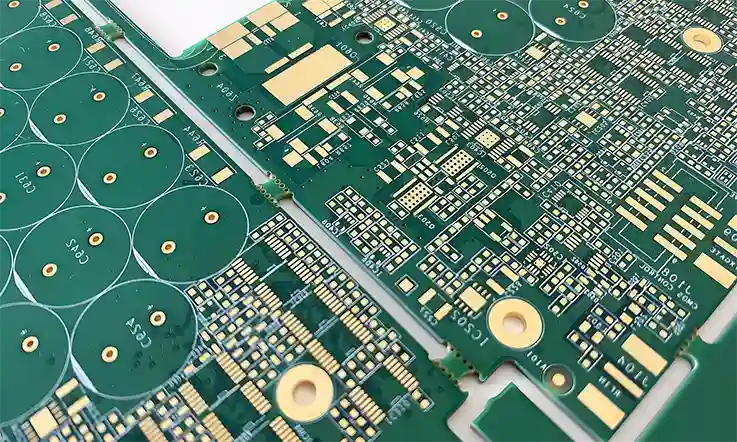
●Image Transfer and Etching: High-resolution imaging processes define the circuit patterns. Etching parameters are tightly controlled, allowing copper traces to achieve the exact widths and spacing required for RF, LED, and power circuit designs.
●Thermal Via Drilling and Plating: CNC drilling equipment forms vias at locations designated to extract heat from high-power components. A thorough copper plating process creates robust, continuous thermal paths from the circuit layer to the aluminum base.
●Routing and Profiling: The board’s final shape, including edges and internal cutouts, is machined to strict design tolerances. This prevents stress concentrations that could otherwise affect mounting or long-term operation.
2.Material Specifications and In-Process Validation: Surface finishes, copper thickness, and process validation are fundamental elements in the construction of Hybrid Aluminum PCBs for demanding electronic designs.
●Surface Finishes: Surface treatments such as ENIG (Electroless Nickel Immersion Gold) and OSP (Organic Solderability Preservatives) are offered. These are selected to provide optimal soldering conditions for component attachment and to protect the copper surfaces from oxidation.
●Copper Thickness: Copper foil weight is chosen based on current-carrying requirements and thermal management needs, with common options including 1 oz, 2 oz, and 3 oz. Heavier copper is specified for power circuits that must handle high current loads.
●Process Monitoring: A multi-stage validation methodology is employed. Automated Optical Inspection (AOI) tools review trace paths and clearances after etching, while electrical tests confirm circuit continuity. These in-process checks verify dimensional accuracy and lamination quality before the boards proceed to the next stage.
3.Logistics: Lead Times and Scalability:The fabrication of Hybrid Aluminum PCBs is planned to match project schedules while maintaining accuracy alongside manufacturing efficiency.
●Lead Time Considerations: Project timelines are influenced by layer count, material choices, and design complexity. Many projects move from design approval to shipment within 8 to 18 working days, depending on the specific stack-up and testing protocols.
●Volume Scalability: For high-volume projects like LED lighting arrays and EV modules, work is organized in batches that uphold precise layer alignment and via quality across every panel. Flexible, smaller-batch options for prototypes and design verification runs are also maintained, supporting engineers who need to test designs before committing to mass fabrication.
Design for Manufacturability (DFM): Avoiding Common Fabrication Pitfalls
A successful Hybrid Aluminum PCB project originates from an understanding of the interplay between design intent and fabrication realities. Implementing robust DFM principles is a foundational step to achieving optimal performance, reliability, and cost-effectiveness.
Managing CTE Mismatch and Mechanical Stress
A primary DFM consideration is managing the different Coefficients of Thermal Expansion (CTE) among the materials in the stack-up. This mismatch is an inherent physical challenge that must be addressed at the design stage.
●The Technical Challenge: During thermal excursions, from the high temperatures of solder reflow to the operational cycling in the end environment, these materials expand and contract at different rates. This differential movement creates mechanical stress, particularly at the material interfaces. Over time, this stress can manifest as via barrel fatigue or cracking, pad lifting, or delamination of the dielectric from the aluminum core, ultimately leading to field failures.
DFM Mitigation Strategies:
●Symmetrical Stack-up Construction: The creation of a symmetrical layer stack-up is strongly advised. Balancing the copper distribution and dielectric layer thicknesses relative to the central aluminum plane helps to distribute stress forces evenly. This balanced construction is the most effective method for preventing board warpage and enhancing long-term structural stability.
●Appropriate Dielectric Material Selection: The use of specialized, thermally conductive dielectrics that possess a degree of mechanical compliance is beneficial. These materials, often polymer-ceramic composites, can absorb a portion of the shear stress generated between the rigid copper traces and the aluminum base, preserving the integrity of the bond line.
●Design of Robust Via Structures: Vias in Hybrid Aluminum PCBs are subjected to significant z-axis stress. Designing vias with adequate annular ring specifications and ensuring a high-quality, uniform copper plating process are requirements for withstanding the rigors of thermal cycling.
Application Example: A project initially exhibited a 1.5% assembly yield loss due to board warpage after reflow. The root cause was identified as an asymmetrical 4-layer stack-up with 2oz copper on the top layer and only 1oz copper on the bottom. A DFM review led to a redesigned stack-up with balanced 2oz copper on both outer layers. The revised design eliminated the warpage issue, resulting in a near-zero yield loss from this failure mode and demonstrating the direct financial benefit of proper DFM.
Optimizing Thermal Via Design and Placement
Thermal vias function as the primary conduits for vertical heat transfer, but their design and implementation demand careful engineering to be effective and to avoid introducing assembly defects.
●The Technical Challenge: An improperly designed via array can be inefficient at heat extraction or may compromise the structural integrity of the component’s solder pad. An excessive number of open vias can lead to solder wicking during the assembly process, where solder is pulled down into the via barrel, starving the joint and creating a weak or open connection.
DFM Mitigation Strategies:
●Direct Thermal Path Placement: For maximum effectiveness, thermal vias must be placed directly beneath the thermal slug or pad of the heat-generating component. This creates the shortest, most direct path for heat to escape to the aluminum substrate.
●Application of Via-in-Pad Technology: The recommended approach for high-power applications is to use via-in-pad techniques. This involves filling the vias with a specialized conductive or non-conductive epoxy and then plating them over (capping) to create a flat, co-planar surface. This methodology provides an ideal surface for soldering fine-pitch components and completely prevents solder wicking.
●Calculated Via Array Density: The quantity, diameter, and pitch of the vias should be determined based on thermal modeling and the specific thermal load of the component. It represents a balance: providing sufficient thermal conductivity without overly perforating the pad and compromising the solder joint’s mechanical strength.
Defining Electrical Clearances and Routing Constraints
The presence of a large, conductive aluminum plane introduces unique electrical isolation requirements that are not present in standard FR-4 designs. These must be respected to prevent catastrophic electrical failures.
●The Technical Challenge: Insufficient electrical clearance between copper features (such as traces, pads, or power planes) and the edge of the aluminum core or any internal cutouts can result in dielectric breakdown and electrical shorting, a risk that increases with operating voltage.
DFM Mitigation Strategies:
●Establish Generous Edge Clearances: A specified minimum clearance must be maintained from all routed copper features to the physical routed edge of the board and to any internal cutouts or non-plated holes. This distance is a function of the application’s maximum operating voltage and is a requirement to pass high-potential (HiPot) testing.
●Employ Controlled-Depth Routing and Drilling: When fabricating mounting holes or other features that must not make electrical contact with the aluminum core, precise controlled-depth machining processes are used. These techniques ensure that the cutting tool removes the copper and dielectric layers without penetrating into the aluminum substrate, thereby maintaining electrical isolation.
●Incorporate Clear Fabrication Notes: All such specific clearance and machining requirements must be explicitly detailed in the fabrication drawings and notes. This clear communication enables CAM engineers to correctly program the manufacturing equipment and ensure the design intent is perfectly executed.
Advanced Validation and Validation for Long-Term Reliability
Meeting industry standards like IPC and UL is the baseline for quality. For applications where long-term reliability is non-negotiable, it is necessary to go beyond standard pass/fail tests and employ advanced validation methods to simulate a product’s entire operational life.
Accelerated Life Testing for Reliability Projection
These tests subject the PCB to conditions far harsher than its expected operating environment to simulate years of use in a matter of days or weeks, proactively identifying potential failure modes.
Highly Accelerated Life Test (HALT):
HALT is a destructive testing method used during the design validation phase. It subjects a board to progressively higher levels of thermal shock and random vibration until failure occurs. The goal is not to see if it passes, but to find the fundamental operational and destruct limits of the design. This data is invaluable for understanding design margins and identifying the weakest points in the construction.
Thermal Shock Testing:
Unlike gradual thermal cycling, thermal shock testing involves plunging the board between extreme temperature chambers (e.g., from -65°C to +150°C) in a matter of seconds. This puts immense stress on the via structures and material interfaces. By performing hundreds or thousands of these cycles and then conducting cross-sectional analysis, it’s possible to evaluate the board’s resistance to via barrel cracking and delamination caused by CTE mismatch.
Electrical Integrity Under Environmental Stress
These tests evaluate how the board’s electrical properties hold up when subjected to challenging environmental conditions that can promote degradation over time.
| Test Name | Test Conditions | Measured Parameter |
| Surface Insulation Resistance (SIR) Testing | High temp & high humidity (e.g., 85°C / 85% RH, 1000 hours) | Dielectric resistance between conductors |
| Conductive Anodic Filament (CAF) Testing | Elevated temp, humidity & voltage bias (accelerated conditions) | Susceptibility to CAF growth |
Surface Insulation Resistance (SIR) Testing:
SIR testing measures the electrical resistance of the dielectric material between adjacent conductors. The test is performed under high temperature and high humidity conditions over an extended period (e.g., 1000 hours). A stable, high resistance value confirms that the dielectric material and solder mask are resistant to electrochemical migration and will not cause leakage currents or short circuits over the product’s lifetime.
Conductive Anodic Filament (CAF) Testing:
CAF is a failure mode where a conductive filament grows along the glass fibers within the dielectric material, eventually causing a short between vias or plated holes. CAF resistance testing subjects the board to high temperature, high humidity, and a continuous voltage bias to determine its susceptibility to this failure mechanism. This is a qualification for high-density, high-voltage applications.
Advanced Material and Structural Analysis
These analytical techniques provide a microscopic view of the board’s construction quality, offering information that is impossible to see with non-destructive methods and providing definitive proof of quality.
Cross-Sectional Analysis (Microsectioning):
This is a destructive but highly informative process where a slice is cut from a finished board, mounted in an epoxy puck, and polished to a mirror finish. Viewed under a high-magnification microscope, it allows for precise measurement of copper plating thickness in via barrels, assessment of layer-to-layer registration, verification of lamination quality (checking for voids), and inspection for drilling defects like smear or resin recession.
Scanning Electron Microscopy (SEM) and Energy-Dispersive X-ray Spectroscopy (EDS):
For failure analysis or advanced material qualification, SEM can provide extremely high-magnification images of fracture surfaces or material interfaces. When combined with EDS, it can identify the elemental composition of materials, which is useful for contamination analysis or verifying material specifications.
Cost Structure Analysis: Key Factors in PCB Pricing
Understanding the cost drivers behind Hybrid Aluminum PCBs allows engineers and procurement teams to guide design and purchasing choices effectively. The price of these specialized boards directly reflects the selected materials, the complexity of the layout, and the manufacturing steps needed to reach the required performance.
Material Selection as a Primary Cost Driver
The raw materials constitute a substantial portion of the board’s final cost. The choices made at the design stage have a direct and significant impact on the price.
●Aluminum Substrate: The thickness and alloy type of the aluminum base are direct cost factors. A thicker substrate (e.g., 3.0mm) for high thermal loads will be more expensive than a thinner one (e.g., 1.0mm) due to higher material volume. Furthermore, high-performance alloys may carry a premium over standard grades like 5052.
●Thermally Conductive Dielectric: The dielectric material that isolates the copper from the aluminum is one of the most specialized and costly components. Materials with higher thermal conductivity (lower thermal resistance) command higher prices. The selection must balance thermal performance requirements against budgetary constraints.
●Copper Weight: The thickness of the copper foil (copper weight) directly influences cost. A board specified with 3 oz copper will be more expensive than one with 1 oz copper due to the higher commodity price of copper and the longer processing times required for etching thicker foils.
Design Complexity and Layer Count
Beyond raw materials, the complexity of the design itself is a major factor in the cost calculation.
●Number of Layers: Each additional copper layer adds multiple process steps, including lamination, imaging, and etching. Consequently, a four-layer hybrid board will be substantially more expensive than a two-layer design with a similar footprint.
●Minimum Trace and Space: Designs that push the limits of fabrication with very fine lines and spaces (e.g., below 4 mils or 0.1mm) require more advanced high-resolution imaging equipment and tighter process controls. This leads to lower yields and higher per-unit costs compared to designs with more generous feature sizes.
●Hole Density and Smallest Hole Size: The total number of drilled holes and the size of the smallest hole affect the time spent on CNC drilling machines. High-density designs with numerous small-diameter vias increase machine time and tooling costs.
Fabrication Processes and Surface Finish
The specific manufacturing and finishing steps chosen for a board can also alter its final price.
●Specialized Machining: Requirements for controlled-depth drilling, controlled-depth routing, or complex internal cutouts add significant machining time and complexity, which is reflected in the cost.
●Via-in-Pad Processing: Filling and capping vias (via-in-pad planarization) is a multi-step process that adds considerable cost compared to standard open or tented vias. However, it is often a technical requirement for assembling complex components like BGAs.
●Surface Finish: The choice of surface finish has a direct cost implication. OSP is typically the most economical option. ENIG provides superior performance and a flatter surface but is more expensive due to the cost of gold and the complexity of the electroless plating process.
Order Quantity and Panelization Efficiency
The economics of PCB fabrication are heavily influenced by volume and efficiency.
●Economies of Scale: Larger order quantities allow for greater automation and process optimization, significantly reducing the per-unit cost. The setup costs are amortized over a larger number of boards.
●Panel Utilization: The efficiency with which individual boards can be arranged on a standard manufacturing panel affects material waste. A design that utilizes the panel area efficiently will have a lower per-unit cost than an awkwardly shaped board that leads to significant material scrap.
Turnkey Assembly Services for Aluminum-Backed PCBs
Hybrid Aluminum PCBs require specialized assembly processes to realize their full potential. By integrating precision component placement with the unique thermal properties of aluminum substrates, assemblies are built for uninterrupted operation in advanced applications.
Full Turnkey Assembly for Complex Designs
Turnkey assembly services are specifically designed for the complexities of Hybrid Aluminum PCBs, accommodating their unique stack-ups and thermal management requirements from procurement to final testing.
●Component Sourcing and Management: The process begins by aligning the Bill of Materials (BOM) with the layout, ensuring the design supports optimal placement of all SMT and through-hole components before procurement.
●SMT and Reflow Profiling: Recognizing that aluminum substrates affect heat distribution, controlled thermal profiling is utilized during reflow. This process ensures high-quality solder joints and protects component integrity across power stages and LED modules.
●Precision and Selective Soldering: For designs requiring mixed technologies, selective soldering processes are adapted to the specific copper thickness and pad geometry, protecting layer integrity and nearby thermal vias during the assembly of through-hole components.
Rapid Prototyping and Small-Batch Orders
Understanding that design validation is a frequent requirement before committing to volume fabrication, rapid prototyping and small-batch assembly workflows address this need efficiently.
●Fast-Turnaround Prototyping: By leveraging an inventory of pre-verified aluminum substrates and copper laminates, sample builds can be completed in shortened cycles. This provides functional boards for testing LED arrays, validating RF drivers, and verifying power module performance.
●Small-Batch Assembly Runs: Pilot runs allow an engineering team to evaluate thermal pathways, stack-up performance, and circuit behavior under operational loads, providing the data needed to refine a design before scaling.
●Iterative Testing and Support: Each prototype or small-batch run can undergo full thermal and electrical testing. This confirms heat management efficiency and circuit integrity, supporting precise layout and component refinements for the next design iteration.
Specialized Assembly for Specific Applications
Assembly workflows are optimized for the distinct demands of the most common applications for Hybrid Aluminum PCBs, ensuring maximum performance and reliability for each use case.
●LED Array Assembly: For LED modules, the entire process is managed to achieve even brightness and superior heat dissipation. Specialized SMT lines ensure precise LED alignment and optimal solder conditions across the entire array.
●Power Electronics Integration: Inverter and drive control circuits require boards that can manage high current delivery. Assembly steps are tuned to handle heavy copper planes and protect the board’s thermal management system during integration.
●RF and High-Frequency Modules: For RF circuits, controlled thermal conditions are a priority. Precise assembly techniques produce high-fidelity connections that preserve the board’s specified impedance and thermal benefits.
Future Outlook: Emerging Trends in Metal Core PCB Technology
The field of thermal management is in continuous evolution, driven by the push for smaller, more powerful, and more efficient electronics. Hybrid Aluminum PCB technology is adapting and advancing to meet these future challenges.
Integration with Next-Generation Power Semiconductors
The adoption of wide-bandgap semiconductors like Gallium Nitride (GaN) and Silicon Carbide (SiC) is reshaping power electronics, creating new demands for thermal substrates.
●The Synergy: This increased power density generates even more concentrated heat, making the advanced thermal dissipation of Hybrid Aluminum PCBs more valuable. Future board designs will focus on hyper-optimized thermal paths with ultra-low inductance, designed specifically to maximize the high-frequency switching performance of GaN and SiC devices. The co-design of the PCB and the semiconductor package will become standard practice.
Advancements in Thermally Conductive Dielectric Materials
The performance of the dielectric layer directly gates the overall thermal efficiency of the stack-up. Research and development in this area are yielding results that promise to push performance boundaries.
●Ultra-Thin Dielectrics: The development of ultra-thin (e.g., < 50µm) dielectric layers with extremely high dielectric strength and thermal conductivity will further reduce the thermal resistance between the copper circuit and the aluminum core. This allows for even more efficient heat transfer in a thinner overall profile.
●Novel Filler Materials: Researchers are exploring next-generation ceramic and composite filler materials, including engineered diamond particles and other exotic materials, to push thermal conductivity values to new heights, approaching the performance of much more expensive ceramic substrates.
3D and Formable Metal Substrate PCBs
The demand for electronics to conform to non-flat surfaces is driving innovation in formable PCBs, moving beyond the traditional two-dimensional plane.
●The Concept: Instead of a flat aluminum plate, the substrate can be pre-formed or stamped into a three-dimensional shape. The flexible circuit layers are then laminated onto this non-planar surface. This allows the PCB to become an integral part of the product’s structure, saving space and eliminating separate mounting hardware while still providing excellent thermal management.
Embedded and Integrated Cooling Solutions
As power densities continue to rise, some applications may require thermal performance beyond what a passive metal substrate can offer. This is leading to the integration of active cooling features directly within the PCB.
●Embedded Heat Pipes: Miniaturized, flat heat pipes can be embedded within the aluminum substrate during the lamination process. These devices use a two-phase heat transfer cycle to move heat away from a source with incredible efficiency, offering a significant performance boost over pure conduction.
●Microchannel Liquid Cooling: For the most extreme applications, micro-channels can be machined directly into the aluminum substrate, allowing a liquid coolant to flow through the board and directly absorb heat from beneath the power components. This represents the pinnacle of integrated thermal management.
Why Choose JarnisTech to make your Hybrid Aluminum PCBs Project?
Selecting a fabrication and assembly specialist for high-performance thermal PCBs is a decision based on demonstrated capability and process control. JarnisTech’s approach is built upon five pillars designed to deliver predictable outcomes and engineering value for complex projects.
A Commitment to Uncompromising Quality
Quality is not a final inspection step; it is a philosophy embedded in every stage of the process. Adherence to stringent industry standards is the baseline. All fabrication conforms to IPC-A-600 Class 2 or higher standards, and the entire quality management system is certified to ISO 9001. This procedural rigor is complemented by the advanced validation methods detailed previously, including cross-sectional analysis and thermal shock testing, to verify that the final product not only meets but exceeds design specifications for long-term reliability.
A Transparent and Competitive Pricing Structure
The pricing philosophy is built on transparency and value. The “Cost Structure Analysis” section of this guide outlines the technical drivers of cost, and all quoting reflects this engineering-based approach. The objective is to achieve the lowest Total Cost of Ownership (TCO) for the client. This is accomplished through proactive DFM reviews that identify potential cost-saving opportunities in material selection or design optimization without compromising performance. The outcome is a competitive pricing structure that supports the technical needs and budget goals of each project.
Dependable and Agile Lead Times
Project timelines are supported through clear communication and streamlined workflows. The fabrication setup is designed to handle both rapid prototyping and large-scale volume builds. Prototype runs for design checks can be arranged on fast-track schedules. For volume quantities, batch processing and dedicated lines enable reliable output across thousands of boards. This flexibility helps engineering groups transition from initial testing to full-scale builds without unnecessary delays.
Responsive, Engineering-Led Service
Every project benefits from direct access to engineering expertise. The service model is collaborative, functioning as an extension of the client’s design team. The complimentary DFM consultation is a cornerstone of this approach, aiming to optimize designs for performance, manufacturability, and cost before fabrication begins. This engineering-focused support remains active throughout the project, addressing technical challenges with clear, targeted solutions.
“The DFM support from JarnisTech was instrumental during our design phase. Their recommendations on stack-up symmetry not only solved a potential warpage issue but also improved the thermal performance beyond our initial simulations. This level of proactive engineering is rare.” – Senior Hardware Engineer, Industrial Controls Sector
Advanced Manufacturing and Assembly Capabilities.
The execution of complex Hybrid Aluminum PCB designs requires specialized equipment and deep process knowledge. JarnisTech’s capabilities encompass the full range of advanced techniques discussed in this guide. This includes multi-layer lamination of dissimilar materials, fabrication with heavy copper weights exceeding 3 oz, precision-controlled depth routing and drilling, and the implementation of via-in-pad planarization for high-density components. The in-house turnkey assembly services feature customized SMT reflow profiling specifically for thermally demanding aluminum substrates, ensuring high-yield, reliable solder connections for every component.
Request a Quote for Your Hybrid Aluminum PCB Project
Engaging with a supplier capable of delivering high-performance boards with precise stack-up control and effective thermal pathways is the first step in advancing a project. Structured quoting and engineering support are available for both fabrication and assembly.
Free Engineering Consultation and Design Review
The process can begin with a direct, personalized consultation to help refine a Hybrid Aluminum PCB design before moving to fabrication. This complimentary service is designed to optimize your project for success.
●Design File Review (DFM/DFA): Engineers review Gerber files, Bill of Materials (BOM), and stack-up plans. They check for manufacturability and assembly considerations to ensure copper routing aligns with thermal dissipation goals.
●Thermal Simulation Analysis: Advanced simulation checks can be performed to validate heat transfer efficiency, confirming the synergy between the aluminum substrate and copper layers for specific power and LED applications.
●Material and Stack-Up Guidance: Recommendations on aluminum thickness, prepreg selection, and copper weight are provided to match design goals with the project’s heat load while helping achieve stable fabrication results during Hybrid Aluminum PCB builds.
Prototyping and Volume Capabilities
A seamless path from initial design validation to full-scale production is available, ensuring quality at every stage.
●Rapid Sample Builds: Quick-turn prototypes can be prepared for LED, automotive power, and industrial systems, allowing for early-stage performance and thermal validation.
●Process and Material Integrity: Lamination and pressing processes utilize specified copper and aluminum layers with precision, upholding high standards of quality in both prototypes and full-scale runs.
●Flexible Scaling: After validation, a project can transition seamlessly from samples to high-volume batches. This allows for integration into LED lighting, EV, and industrial automation workflows without redesign delays.
Information for Your Quote Request
To receive an accurate and timely quote for fabrication and assembly, please have the following information and files ready.
●Gerber Files: For all copper, solder mask, and silkscreen layers.
●Bill of Materials (BOM): With complete part numbers, reference designators, and quantities.
●Pick-and-Place Data (Centroid): For all surface-mount components to facilitate automated assembly.
●Special Requirements: Please note any specific thermal, electrical testing, or mechanical needs for your project.
Contact for a Tailored Solution
A Hybrid Aluminum PCB project deserves a clear path from request to delivery. A straightforward and responsive process is available.
●Direct Communication: The quoting process is designed to clearly define stack-up requirements, copper weights, aluminum thickness, and surface finishes.
●Tailored Delivery Options: Flexible global logistics are offered, with all boards delivered in protective packaging to support project timelines.
●Ongoing Engineering Support: Support is available throughout the quoting and fabrication cycle to help align a design for optimal performance and manufacturability.
FAQ about Hybrid Aluminum PCBs
Q: What is the main advantage of a Hybrid Aluminum PCB compared to a standard FR-4 board with an external heat sink?
A: They provide superior, integrated heat dissipation in a more compact structure, eliminating the need for a separate heat sink and its associated assembly step.
Q: What is the typical maximum operating temperature for a Hybrid Aluminum PCB?
A: Typically 130°C to 170°C, depending on the specific dielectric material selected.
Q: Can blind and buried vias be used in multilayer Hybrid Aluminum PCB designs?
A: Yes, they can be integrated into multilayer designs to increase routing density.
Q: Are there special requirements when panelizing Hybrid Aluminum PCB designs?
A: Yes. Due to the aluminum core, separation is typically done using V-scoring or CNC routing. When designing the panel, adequate space must be left for routing paths, and breakaway tabs must be strong enough to support the panel’s weight.


