
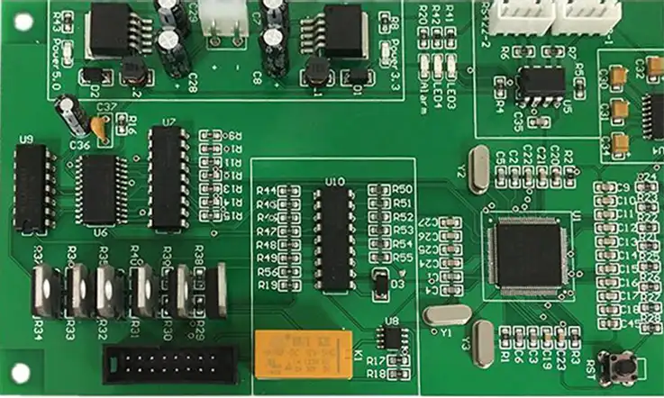
Printed circuit boards, also known as PCBs, have become an essential part of many electrical and electromechanical systems that are in widespread use today. The continuous growth in the demand for PCBs can be attributed to the significant advances made in electrical technology and its applications in various fields. Without PCBs, devices are unlikely to function correctly. Therefore, it is critical that the layout and wiring of the circuit boards are perfect, given that the functionality of the product depends on them. As such, one of the most crucial aspects is ensuring that these circuit boards are correctly designed and manufactured.
Choosing the best way to assemble a circuit board involves considering various factors, especially in the current technological era where PCBs are becoming increasingly intricate, portable, and lightweight. To follow assembly recommendations, it is imperative to prioritize PCB design. This approach results in reduced development costs, a reduction in time to complete products, and seamless transitions between prototype and production stages. If you are interested in PCB design guidelines for assembly and their usefulness, kindly continue reading this post until the end.
What Is PCB Design for Assembly (DFA) ?
PCB Design for Assembly (DFA) is the process of designing a printed circuit board (PCB) in a manner that optimizes the efficiency and reliability of its assembly and manufacturing processes. DFA aims to reduce the assembly time, minimize the number of components required, simplify the assembly process, and ensure maximum quality control during the entire product development cycle.
For this reason, designers incorporate specific features and processes that can make the PCB design more amenable to the assembly and manufacturing of the product. DFA considerations include optimizing the component placement, selecting components that are easy to assemble, minimizing the number of solder joints, ensuring correct orientation of components, and facilitating inspectability and testing during assembly. Proper implementation of DFA can result in reduced production cycle times, lowered costs, and more reliable products.
How Many Assembly Stages for PCB Design for Assembly ?
Printed circuit board (PCB) customers who outsource the design and production of their PCBs prioritize the Printed Circuit Board (PCB) Design for Assembly (DFA) process. Proper implementation of this process reduces development costs, shortens the production cycle, and ensures a smooth transition from the prototype phases to production.
In designing a PCB, it is essential to bring future needs into consideration to ensure proper construction, prototyping, and production. By planning ahead, the production cycle can be shortened, development costs reduced, and transitions from prototype to production phases made smoother. DFA refers to the process of including certain processes into a Design for Manufacturing (DFM) routine for PCB development. Before delving into specifics of what defines good PCB DFA, it is vital to understand the significance it holds in creating PCB products.
PCB design and development involve two assembly stages, including PCB prototype assembly and PCB production assembly. During the PCB design phase, both stages should be incorporated into DFA to ensure that PCBs are properly constructed, prototyped, and produced.
Prototype PCB Assembly
PCB Design engineers know that in constructing the board prototype, it is essential to verify the accurate attachment of components. Besides adhering to clearance and tolerance criteria, the design must also comply with clearance and tolerance specifications. During the design phase, PCB Design engineers prioritize additional DFA measures, including proper component spacing, component labeling, and solder mask application. This approach guarantees an efficient assembly and manufacturing process that leads to a successful PCB product.
● Thermal relief should be adequate.
● Components should match their pads.
● Correct application of solder mask guidelines.
● Board edge clearance rules should be applied.
● The spacing of the components should be adequate.
● The markings and identifications of the components are exact and precise.
● Rules for drill-holes, including aspect ratio and hole tolerance, need to be applied.
Production Assembly
PCB assembly manufacturers undertake all the necessary steps required for prototype assembly. They consider factors such as the reliability of components, requirements for mass production, and the testability of components, among others. Adherence to the DFA standards outlined in the following paragraphs is of utmost importance during prototype assembly. This ensures that the assembly and manufacturing process is efficient, leading to a successful production of the high-quality PCB product.
● Availability of components.
● The board allowing penalization.
● Appropriately defining quality controls.
● The layout withstanding extreme conditions
IPC PCB Assembly Standards
As a PCB manufacturer, we follow various IPC assembly standards to ensure the provision of high-quality services to our clients. We adhere to the following additional IPC assembly standards while assembling our client’s boards:
● IPC-A-630: This standard defines the guidelines for electronic enclosure specifications. During the assembly and inspection process, our team strictly adheres to this standard.
● IPC-A-600: More commonly known as IPC-600, this standard specifies acceptance requirements for each product category. It outlines what is desirable, permissible, and non-negotiable regarding the board’s requirements.
● IPC/WHMA-A-620C: This standard provides a detailed description of cable and harness assemblies, including the materials, processes, tests, and acceptability criteria. Our team ensures strict adherence to this standard during the assembly of cable and harness assemblies.
PCB Design For Assembly (DFA) Guidelines: 8 Steps
During the design stage of a board and its components, it is important for PCB design engineers to consider certain guidelines that facilitate the efficient and seamless assembly of the board and its components.
Step 1: Use Standard and Common Components
Using readily available and common components ensures their continued production and availability, thus avoiding unnecessary delays caused by end-of-life (EOL) components. Standard and common components are also less expensive and of higher quality, reducing inventory costs and the risk of poor quality.
Step 2: Component Spacing Rules
It is essential to design the board ensuring that the components are appropriately spaced, neither too close nor too far from each other. Overlapping components cause interference and may require a redesign of the layout. A recommended best practice is to ensure that the footprint design allows for ample space between the edges of each component to minimize spacing problems.
Step 3: Component Orientation and Handling
The board should be designed so that components are assembled consistently in the same orientation. Component orientation has a significant impact on board buildability, soldering techniques, types of thermal reliefs required, and signal quality. Placement considerations are essential to minimize issues such as electrical noise from components located too closely to one another. Additionally, drill holes should not be placed near the board’s edge as that could cause the board to shatter during the manufacturing process.
Step 4: Follow Datasheet Precisely When Designing Footprints
To ensure that the footprints are precise and accurate, it is crucial to follow the datasheet guidelines strictly. Doing so results in the creation of proper identifications and footprints, thereby reducing the possibility of pad mismatches. Failure to adhere to datasheet recommendations may result in inaccurate footprints, requiring a complete redesign of the boards and subsequent refabrication. As a PCB design engineer, following datasheet guidelines is essential to ensure the successful and timely completion of the board design and its manufacturing process.
Step 5: Updated Bill of Materials (BOM)
The accuracy and completeness of the bill of materials (BOM) is of great importance in ensuring that projects are completed on schedule. Any revisions or updates to the design must be reviewed, and the BOM should be updated accordingly, with the correct number, description, and values for each component.
Step 6: Operating Environment
The PCB’s operating environment must be taken into account during the design process to ensure that it functions reliably in the given condition. For instance, through-hole components may be a more reliable option than surface mount devices (SMDs) in situations where there is excessive movement and vibration.
Step 7: Thermal Relief
To enable proper functioning, the PCB’s electronic components must dissipate heat produced during operation. Thermal dissipation of heat from soldering is also necessary. Therefore, the board should be designed to facilitate fast heat dissipation and remain functional during soldering.
Step 8: Track Routing Techniques
Designs should adhere to established guidelines to prevent interference with the board and other components’ positioning. For example, trace edges should be a minimum of 0.025 inches away from the board’s edge to avoid inadequate solder connections. Proper alignment of traces with pads or vias is also critical to prevent flawed solder connections. As a PCB design engineer, it is prudent to follow professional track routing techniques to ensure efficient and reliable board configurations.
PCB Layout Techniques for DFA
Here are some PCB layout techniques for Design for Assembly (DFA) to optimize the design for ease of assembly:
● Component Placement: Place components logically and with care, grouping similar components together. Optimize the layout placing closely spaced components and keeping them aligned on a single axis. Try to avoid placing through-hole and surface mount components on the same side of the board.
● Footprint Design: Ensure footprints are correctly sized, accurately aligned, and provide clearance for automated equipment to place components. Make sure critical pins are visible and accessible for inspection.
● Trace Routing: Minimize trace bends, keep traces as short as possible and use a modern design tool. Using a 45-degree angle reduces the number of turns, improving signal flow and provides access by the placement equipment and inspection equipment.
● Component Orientation: Keep all polarized components mounted in the same orientation. Use polarity markings and silkscreen to minimize placement errors.
● PCB Stack-Up: Consider the PCB stack-up, layer requirements, and termination pad size when choosing component footprints. Layer count should be reasonable to keep the manufacturing process simple and cost-effective.
● Panelization: Use panelization to increase throughput, lower costs and speed up the assembly process. Ensure the panel layout does not affect the performance or reliability of the final product.
● Thermal Considerations: The thermal characteristics of components should be a significant consideration when designing for assembly. Ensure heat is adequately dissipated or removed, so the components do not overheat or become damaged.
Testing and Inspection of DFA
Testing and inspection are essential in the Design for Assembly (DFA) process to ensure that the PCB is assembled correctly, is reliable, and meets or exceeds all requirements. Here are some common testing and inspection techniques used for DFA:
● In-Circuit Testing (ICT): ICT is a popular testing method used to verify that the electrical components of a PCB are correctly connected and functioning as intended. This automated test uses bed-of-nails fixtures to test individual nodes, pins, or vias.
● Functional Testing: This type of testing is performed to check that the PCB is working as intended. It checks whether the PCB meets or exceeds all requirements and performance assays for different protocols.
● Automated Optical Inspection (AOI): AOI machines use cameras and computer-assisted vision to scan the PCB surface for defects, such as misalignments, polarity issues, and missing or incorrect components.
● X-Ray Inspection: X-Ray equipment can examine PCBs by emitting radiation through the board to check for issues such as cold solders, bridging or incorrect component placement.
● Manual Inspection: Visual inspection of the assembly can help detect issues such as damaged components or solder joints or incorrect polarity orientation. It takes less time than automated methods but can be less accurate as it can depend on the operators.
Tools and Software for DFA
There are many tools and software available for Design for Assembly (DFA) that designers can use to optimize PCB designs for ease of assembly. Here are some popular tools and software for DFA:
● 3D Modeling Software: 3D modeling software can help visualization and simulate board layout in the system. It can identify potential assembly issues that are not easily noticeable in 2D layouts.
● CAD Software: Popular CAD software such as Altium, Eagle, and KiCAD can incorporate design-for-assembly guidelines and generate design rules to optimize the PCB layout.
● Automated Optical Inspection (AOI) Software: Automated optical inspection software is used to inspect the PCBs for manufacturing defects using camera-based instruments. It can help monitor soldering quality, identify defects and improve yield rates.
● Design for Manufacturability (DFM) Software: DFM software has built-in design guidelines that have an implicit set of rules to facilitate manufacturing issues. It provides warnings if certain guidelines are not met,
● Simulation Software: Simulation software models various manufacturing processes such as soldering and assembly to identify failure modes, estimate defects, and improve manufacturing yield.
● Design Validation Software: This software ensures that designs adhere to industry standards and guidelines. It checks the PCB design for electrical, mechanical, and physical performance.
Importance of DFA in PCB Manufacturing
Design for Assembly (DFA) plays a crucial role in the PCB manufacturing process as it helps to optimize the design for ease of assembly, reduce the overall cost of manufacturing, and improve quality. Here are some specific reasons why DFA is important in PCB manufacturing:
● Cost Savings: DFA helps to identify potential design flaws that could increase the cost of manufacturing, such as complicated routing and assembly steps, component placement issues, or excessive board real estate. Optimizing a design for assembly can significantly reduce manufacturing costs, as well as minimize the number of components required for the board.
● Quality and Reliability: A design optimized for assembly is less prone to errors during the assembly process, reducing the likelihood of manufacturing defects or reliability issues later down the line. A well-designed PCB can also improve signal integrity and reduce electromagnetic interference (EMI) that could impact the board’s performance.
● Time-to-Market: Streamlining the assembly process through DFA can reduce the time it takes to bring a product to market. This can help a company stay competitive in a fast-moving industry, especially if they are able to produce high-quality, low-cost products more quickly than their competitors.
● Manufacturing Flexibility: A DFA-optimized design can make assembly easier, allowing manufacturers to more easily adapt to new production runs, make last-minute modifications, or switch suppliers without significant changes to the overall process.
By implementing DFA principles, designers can create printed circuit board (PCB) designs that are cost-effective, reliable, and easier to manufacture. This, in turn, leads to higher-quality products, faster turnaround times, and ultimately more satisfied customers.
Common PCB Assembly Defects
PCBA manufacturers encounter several common errors and problems during PCBA assembly, which are detailed below. To prevent these flaws, manufacturers employ a range of quality control procedures, some of which are outlined in the following subsections.
● Solder Voids: Solder voids are empty spaces or holes within a solder connection, which forms when insufficient solder is available to create a connection. Typically, air forms the solder void. Quality control measures are implemented to detect and prevent solder voids, ensuring proper solder connections.
● Solder Balls: During surface-mount assembly, a commonly occurring flaw is the formation of solder balls. This occurs when small sphere-like particles of solder separate from the larger body and begin to circulate independently, forming a bridge between two adjacent leads and resulting in functional issues to the board.
● Solder Bridging: Solder bridging arises when solder is placed between two conductors that should not be electrically linked, resulting in unwanted connections and shorts. Quality control measures are implemented to prevent bridging, ensuring proper solder connections and reducing circuit malfunctions.
● Tombstones: Tombstones occur when an SMD component is partially or completely removed from its landing pad. This phenomenon, also known as the Manhattan effect, is a result of force imbalances during reflow soldering and is most common in small SMD passives (packages of 0603 or smaller). Manufacturers implement quality control measures to detect and prevent tombstones, ensuring proper soldering of SMD components.
How JarnisTech Helps You with PCB DFA?
● To quickly correct any DFA issues with your design.
● Provides you with tolerance and clearance requirements.
● Makes available DFA guidelines that you can upload to your design program.
● provides information regarding potential issues that can be avoided by following DFA rules.
● Helps you comprehend the significance of DFA and the appropriate manner in which it need to be utilized.
The absence of PCB DFA in PCB design may lead to future problems with PCB board assembly, including prolonged production cycles, increased costs, and unexpected setbacks during the transition from prototyping to production. Thus, it is vital to apply PCB DFA to ensure successful PCB board manufacturing.
At JarnisTech, we prioritize assisting our clients in adopting good DFA practices by providing accurate DFM details, employing advanced component validation tools, and enabling our clients to view and download DRC files conveniently. For Altium users, these files can be quickly added to their PCB design software. We take pride in our commitment to helping our clients streamline their PCB design and assembly processes while ensuring the highest standards of quality.
Future Trends in DFA
As technology continues to evolve, the future of DFA is likely to see even more emphasis on automation, simulation, and software tools that can assist in the PCB design process. Here are some potential trends to look for in the future of DFA:
● Enhanced Simulation: Sophisticated simulations can help designers to optimize their PCB design for ease of assembly with greater accuracy.
● Integration with CAD software: As PCB design software continues to incorporate DFA principles, designers can expect to have access to more intuitive tools that identify potential assembly issues and make recommendations to enhance the DFA aspects of the design.
● Automation: As more PCB manufacturing processes move towards automation, designers will be able to leverage DFA principles to optimize assembly lines and improve throughput.
● 3D Printing and Additive Manufacturing: 3D printing and additive manufacturing are becoming more popular in the PCB industry. DFA principles will play a vital role in optimizing designs for these manufacturing techniques as they become more widespread.
Therefore, as DFA continues to evolve, designers can expect to have access to more sophisticated tools and technologies to optimize their designs for assembly, resulting in more cost-effective and efficient PCB manufacturing processes.
Final Words
Optimizing PCB design for assembly requires careful consideration of many factors including proper component placement, trace routing, PCB layout, and DFM and DFT practices. By paying attention to each of these areas during the design process, designers can optimize their PCBs for efficient and high-quality assembly, which can result in lower manufacturing costs and a more reliable end-product. It’s important to keep in mind that PCB design is an iterative process and requires collaboration between design, manufacturing, and testing teams to ensure that the final design meets all of the necessary requirements. With a focus on optimizing PCB design for assembly, designers can create robust and reliable electronic circuits that meet the needs of the end-user.
The guidelines outlined above for PCB design and assembly are crucial in ensuring the highest level of quality in PCB manufacturing. If you require PCB services of exceptional quality, it is advisable to partner with an industry leader like JarnisTech. Our company has substantial expertise and a competent team, and we specialize in designing, assembling, and fabricating top-quality, performance-oriented printed circuit boards (PCBs), tailored to your project’s specifications.
As a well-regarded and trusted PCB manufacturer and supplier in China, we take pride in our years of experience and the ability to deliver outstanding services to our clients. Our commitment to supplying premium-quality PCBs to meet the requirements of every application is second to none. We invite you to work with our dedicated team of experts to create exceptional PCBs for your project.


