
The successful operation of core electronic systems depends on the underlying performance of their printed circuit boards. These systems necessitate PCBs capable of withstanding significant thermomechanical stresses while preserving high-speed signal fidelity. Advanced laminates, such as the Shengyi S1140F system, provide the foundational material properties for such applications. The full potential of these materials is only unlocked, however, through a precisely controlled and deeply understood fabrication sequence. This technical brief provides a detailed analysis of the fabrication methodologies required to transform a high-performance substrate into a product of uncompromising reliability, using the S1140F system as a reference.
Core Challenges in High-Reliability PCB Fabrication
The construction of multilayer circuit boards for demanding applications requires the mitigation of several inherent physical and electrical failure modes. As circuit densities increase and operational environments become harsher, these challenges intensify.
Thermomechanical Stress and Interconnect Failure
A multilayer PCB is a composite structure of materials with disparate Coefficients of Thermal Expansion (CTE). During thermal excursions, such as solder reflow or operational power cycling, these materials expand and contract at different rates. This mismatch induces powerful mechanical stresses, particularly in the Z-axis, upon the plated-through-hole (PTH) barrels. Unmitigated, this strain leads to fatigue fractures, pad lifting, and other interconnect defects that result in latent or catastrophic field failures.
Signal Integrity Degradation at High Frequencies
For high-speed digital and RF systems, the PCB substrate functions as an active component within the circuit. The electrical properties of the laminate, specifically the dielectric constant (Dk) and dissipation factor (Df), directly influence signal behavior. Variations in these properties across a board, or their instability with frequency and temperature, can degrade signal integrity, manifesting as increased insertion loss, reflections, timing jitter, and crosstalk. Maintaining controlled impedance across all relevant signal paths is a fundamental requirement.
Long-Term Electrochemical Reliability
Beyond immediate functional performance, a high-reliability PCB must resist degradation from environmental factors. One insidious failure mechanism is Conductive Anodic Filament (CAF) formation. Under conditions of humidity and DC voltage bias, a conductive filament can grow along the glass-resin interface within the laminate, creating a short circuit between two previously isolated copper features.
Advanced Fabrication Methodologies and Engineering Solutions
The conversion of raw laminate into a reliable, high-performance circuit board is a sequence of sophisticated and interdependent processes. Each step is engineered to address the fundamental challenges of PCB fabrication and to build quality into the final product.
The Lamination Cycle: Forging Monolithic Structures
The lamination process fuses individual layers of copper foil and prepreg into a monolithic structure. This stage permanently defines the board’s physical integrity and layer-to-layer registration. A precisely controlled lamination cycle is specified for high-performance materials like S1140F to achieve their target properties.
●Pre-Lamination Conditioning: Material is stored in a climate-controlled environment (<23°C, <50% RH) to inhibit moisture absorption. A pre-lamination bake cycle is often employed to expel any residual moisture.
●Vacuum Press Application: The stacked layers are placed within a hydraulic vacuum press to evacuate trapped air, which prevents voids and delamination in the final board.
●Programmed Thermal and Pressure Profiles: A controlled heat ramp allows the resin to flow predictably and fully encapsulate inner-layer circuitry. Full hydraulic pressure (typically 250-500 PSI) is applied at the point of minimum resin viscosity.
●Cure Dwell and Controlled Cool-Down: The material is held at its target cure temperature for a specified duration for complete polymerization. A slow, controlled cool-down under pressure minimizes the buildup of internal stresses.
Precision Drilling and Via Formation
The creation of reliable plated-through-holes is a multi-stage operation demanding high precision. The quality of the via, which forms the electrical connection between layers, is a primary determinant of the board’s overall reliability.
●Drill Tooling and Parameter Optimization: Specialized drill bit geometries are used for filled materials like S1140F to cleanly shear fibers and resin. Spindle speed, in-feed rate, and retract rate are optimized to prevent resin smear and micro-cracking.
●Positional Accuracy: Advanced optical registration systems and material shrinkage compensation factors are applied to achieve exceptional drill-to-pad accuracy, ensuring annular ring integrity.
Advanced Hole-Wall Preparation: Desmear and Etch-Back
After drilling, the hole wall is contaminated with smeared resin. This smear must be removed to ensure a sound electrical connection to the inner-layer copper pads.
●Multi-Stage Desmear Process: The protocol often involves a plasma treatment cycle using reactive gases, followed by immersion in a chemical bath (e.g., permanganate-based) to chemically remove resin smear.
●Positive Etch-Back for Interconnect Robustness: A more aggressive process that removes a controlled amount of resin and glass from the hole wall. This creates a “three-point contact” for the subsequent plating, forming a strong anchor resistant to Z-axis expansion stress.
Electrolytic and Electroless Plating: Building Robust Interconnects
The plating process deposits the conductive copper pathways onto the board and into the drilled holes. The quality of this deposited copper directly affects the board’s reliability.
●Electroless Copper Deposition: An initial, ultra-thin, conductive layer of copper is deposited over all surfaces, including the non-conductive hole walls, via an autocatalytic chemical process.
●Electrolytic Plating with Reverse Pulse: A DC reverse-pulse plating process is employed to deposit a thick layer of copper with a fine-grained, ductile crystal structure, which is inherently more resistant to cracking under thermal stress.
Substrate Analysis: The Rationale for Specifying Shengyi S1140F
The selection of a laminate material is a foundational engineering decision. The choice of a high-performance substrate like Shengyi S1140F is predicated on its ability to provide a stable platform that enables the successful realization of a reliable, high-performance PCB when subjected to an advanced fabrication process.
Defining Thermomechanical and Electrical Characteristics
The material properties of S1140F directly address the core challenges of high-reliability fabrication. Its formulation provides a synergistic set of attributes that, when properly leveraged by the fabrication process, result in a superior final product.
●Low Z-Axis CTE: Formulated to exhibit a low coefficient of thermal expansion in the Z-axis, directly counteracting the primary failure mechanism for plated-through-holes.
●High Thermal Endurance: A high glass transition temperature (Tg ~170°C) and decomposition temperature (Td >340°C) ensure structural integrity through multiple lead-free reflow cycles.
●Stable Dielectric Properties: Exhibits a stable dielectric constant (Dk) and low dissipation factor (Df), creating a dependable platform for high-speed digital circuits and consistent impedance control.
●High CAF Resistance: The advanced resin chemistry provides robust resistance against Conductive Anodic Filament formation, ensuring long-term insulation integrity.
Thermoelectrical Property Summary:
| Property | Shengyi S1140F |
| Z-Axis CTE | < 3.0% (Measured 50–260°C) |
| Glass Transition Temp (Tg) | ~170°C |
| Decomposition Temp (Td) | >340°C |
| Dielectric Constant (Dk @1GHz) | 4.4 ± 0.05 |
| Dissipation Factor (Df @1GHz) | < 0.015 |
| CAF Resistance | >1000 hrs @85°C/85%RH, >100V bias |
Comparative Analysis Against Alternative Laminates
Understanding the positioning of S1140F relative to other materials clarifies its application space. The following provides a technical comparison.
●Versus Standard FR-4: The primary distinction lies in thermomechanical performance. S1140F’s low CTE provides stability against via strain, where standard FR-4’s high CTE presents a liability. S1140F also offers superior resistance to CAF failures.
●Versus Other High-Tg Laminates: This is a peer comparison where materials exhibit similar high Tg and low CTE values. The differentiating factor often becomes process optimization and deep engineering familiarity with a specific material system like S1140F.
●Versus High-Frequency Substrates: This comparison highlights a trade-off. Materials like those from Rogers offer unparalleled low signal loss (Df) for pure RF designs. S1140F, however, is mechanically more robust and cost-effective, positioning it as an optimal choice for mixed-signal systems.
Laminate Comparison Table:
| Property | S1140F | Standard FR-4 | Other High-Tg Epoxies | High-Frequency Substrates |
| Z-Axis CTE | < 3.0% | > 4.0% | 2.8–3.2% | 1.5–2.5% |
| Tg (Glass Transition Temp) | ~170°C | 130–150°C | 160–180°C | 200°C+ |
| CAF Resistance | Excellent | Moderate | Good | Excellent |
| Df @1GHz | < 0.015 | 0.02–0.025 | 0.014–0.018 | < 0.004 |
| Mechanical Robustness | High | Moderate | High | Low–Moderate |
| Material Cost (Relative) | Moderate | Low | Moderate–High | High |
The Engineering Data Package: Blueprint for Flawless Execution
The transfer of design intent from the engineering team to the board fabrication house is a procedure that demands absolute clarity. An incomplete or ambiguous data package is a primary source of manufacturing errors, leading to delays, cost overruns, and potentially non-functional hardware. A comprehensive engineering data package is the blueprint that enables flawless execution of a high-reliability PCB design.
Core File Formats: ODB++ vs. Extended Gerber (X2)
Modern PCB fabrication relies on intelligent data formats that embed a richer set of information, substantially reducing ambiguity.
●ODB++: This is an intelligent, all-in-one data structure. It contains not just the copper patterns, but also the layer stack-up information, drill data, component placement, and netlist information within a single file hierarchy. Its integrated nature reduces the risk of file mismatch errors that can occur when managing multiple, separate files.
●Extended Gerber (X2): This is the modern evolution of the traditional Gerber format. Unlike older formats, X2 files contain metadata that defines the file’s function (e.g., top copper layer, top solder mask) and the layer stack-up position. When combined with an IPC-D-356 netlist file, it provides a complete and verifiable data set.
The Fabrication Drawing: The Definitive Specification
The fabrication drawing is the master document that contains all specifications not included in the electronic data files. An incomplete drawing forces the board shop to make assumptions, which is unacceptable for high-reliability products. A well-defined drawing should always include the following:
●Material Specification: It must explicitly state the required laminate material (e.g., Shengyi S1140F), including any specific glass styles. Any acceptable alternatives should also be clearly listed.
●Layer Stack-up Detail: A clear diagram showing the sequence of all layers, their thicknesses, and the specified copper weights.
●Hole Chart and Tolerances: A table listing all drill sizes, whether they are plated or non-plated, and the required finished hole size tolerances.
●Controlled Impedance Requirements: A table listing which traces require impedance control, their target impedance value (e.g., 50Ω, 100Ω differential), and the layers they are on.
●Other Specifications: Details on surface finish, solder mask color, silkscreen requirements, and any applicable IPC standards (e.g., “Fabricate to IPC-6012 Class 3”).
The IPC-D-356 Netlist: A Tool for Electrical Verification
The netlist file is a textual representation of the board’s intended connectivity.
●Serves as an independent verification tool. The data from the Gerber files is used to generate a netlist, which is then compared against the designer-supplied IPC-D-356 netlist.
●Identifies issues such as unintended shorts or opens that might have occurred during the design or data export process. . A successful comparison provides high confidence that the design’s electrical integrity is correctly represented in the manufacturing data.
An Analysis of Cost Drivers in Advanced PCB Fabrication
Understanding the factors that influence the cost of high-reliability PCBs allows for more informed design trade-offs. While material choice is one factor, several fabrication-related design decisions have a substantial impact on the final unit price. A design optimized for performance without consideration for these drivers can result in unnecessarily high costs.
Material and Physical Dimensions
The physical size and complexity of the board are primary cost drivers.
●Board Size and Panelization: Larger boards consume more material. The efficiency with which a board can be arrayed onto a standard fabrication panel also heavily influences cost. A design that leads to poor panel utilization results in more wasted material.
●Layer Count and Lamination Cycles: Each additional layer adds material cost and requires additional processing steps. Complex constructions like HDI boards require multiple sequential lamination cycles, with each cycle adding significant cost.
Dimensional Tolerances and Feature Sizes
The tightness of the specified tolerances directly correlates with cost.
●Trace Width and Spacing: Demanding finer lines and spaces requires more advanced imaging and etching processes, and typically results in lower yields, which increases the cost of each good board.
●Registration and Annular Ring: Tighter layer-to-layer registration requirements and smaller specified annular rings necessitate the use of more sophisticated alignment and drilling equipment.
Via and Hole Complexity
The technology used to create vertical interconnects is a major cost variable.
●Mechanical Drilling: Standard plated-through-holes are the baseline. The cost increases with higher aspect ratios (board thickness to hole diameter), as these are more challenging to plate reliably.
●HDI and Microvias: Laser-drilled microvias are a significant cost addition due to the specialized equipment and sequential processing required.
●Back-Drilling: Controlled-depth drilling to remove via stubs is an additional process step performed on a specialized machine, adding cost but improving signal integrity for high-speed applications.
The Framework of Trust: Understanding and Applying IPC Standards
The term “high reliability” is subjective without a common frame of reference. The IPC (Association Connecting Electronics Industries) provides this framework through a series of globally recognized standards that define the requirements for PCB design, fabrication, and inspection. Adherence to these standards is a tangible measure of a product’s quality and the capability of its supply chain.
IPC-6012: The Performance Specification
IPC-6012, “Qualification and Performance Specification for Rigid Printed Boards,” defines three classes of product performance.
●Class 1: General Electronic Products. Reserved for applications where the primary requirement is the function of the completed assembly.
●Class 2: Dedicated Service Electronic Products. Includes products where continued performance and extended life are required, and for which uninterrupted service is desired but not a defining factor.
●Class 3: High-Performance/Harsh-Environment Electronic Products. Includes products where continued high performance or performance-on-demand is a necessity, and where equipment downtime cannot be tolerated. This is the standard for aerospace, medical, and other mission-assurance systems.
IPC-A-600: The Acceptability Standard
IPC-A-600, “The Acceptability of Printed Boards,” is a visual interpretation of the IPC-6012 requirements. It provides photographic examples of target, acceptable, and non-conforming conditions for various board features.
Key Differences between Class 2 and Class 3
Specifying fabrication to Class 3 imposes much stricter requirements than Class 2, directly impacting long-term reliability.
●Annular Ring Breakout: Class 2 may permit a via’s drill to break out of the copper land under certain conditions. Class 3 generally does not allow any breakout.
●Plating Voids: Class 3 has more stringent limitations on the allowable number and size of plating voids in a via barrel.
●Resin Recession and Etchback: Class 3 specifies tighter acceptance criteria for the condition of the hole wall after processing, including requirements for positive etchback to ensure a robust interconnect.
●Cleanliness: Class 3 imposes stricter limits on ionic contamination and other residues that could impact long-term electrochemical reliability.
Adherence to IPC-6012 Class 3 is not just a quality mark; it is a manufacturing philosophy that dictates process controls, inspection criteria, and material selection throughout the entire fabrication sequence.
Surface Finish Selection: An Engineering Trade-off Analysis
The surface finish is the terminal interface between the bare PCB and its components. Its selection dictates solderability, long-term integrity, and signal behavior.
ENIG: The Industry Standard for Solderability and Planarity
This process involves depositing a layer of electroless nickel followed by a thin, protective layer of immersion gold.
●Provides a hard, planar, and highly solderable surface ideal for fine-pitch components.
●Offers an extended shelf life, accommodating complex assembly logistics.
●Mitigates the “black pad” failure mode risk through stringent chemical process control.
ENEPIG: The Apex of Reliability for Wire Bonding
ENEPIG represents a technical evolution of ENIG, incorporating a layer of electroless palladium between the nickel and gold.
●Functions as a diffusion barrier, precluding black pad formation entirely.
●Creates an ideal surface for both gold and aluminum wire bonding, a requirement for certain advanced packages.
●Specified for mission-assurance aerospace, medical, and other high-stakes applications.
Immersion Silver (ImAg): Optimizing for High-Frequency Signal Loss
This finish involves depositing a thin layer of pure silver directly onto the copper pads.
●Offers the lowest insertion loss for RF signals due to the absence of a resistive nickel layer.
●Provides exceptional surface planarity, benefiting fine-pitch component assembly.
●Susceptibility to tarnishing is mitigated through advanced anti-tarnish packaging and strict handling protocols.
OSP: A Cost-Effective, Coplanar Solution for Volume Assembly
Organic Solderability Preservative is a micro-thin, water-based organic compound that selectively bonds to copper.
●Delivers a perfectly flat surface as a chemical coating rather than a metallic plating.
●A cost-effective and environmentally favorable process.
●Best suited for single-pass assembly, as the coating is consumed during each reflow cycle.
Hard Gold: Engineering for High-Wear Mechanical Interfaces
This finish involves electrolytically plating a thick, durable layer of gold alloyed with cobalt or nickel.
●Engineered for extreme durability and wear resistance, not primarily for soldering.
●Specified for high-wear surfaces such as edge-connector fingers or contacts that endure thousands of mechanical cycles.
The Microscopic Domain: Glass Weave Effects on Performance
A PCB laminate is a composite of epoxy resin and woven glass fabric. The style of this weave is a deterministic factor in high-speed signal behavior.
A Review of Common Glass Weave Styles
The industry utilizes several standard glass weave styles, each with a unique profile.
●106 Style: A very loose weave, thin and resin-rich, suitable for the thin dielectric layers in HDI applications.
●1080 Style: A general-purpose, looser weave offering a balance for controlled impedance layers.
●2116 Style: A moderately tight weave providing good all-around performance characteristics.
●7628 Style: A very dense weave specified for its high mechanical strength in thick core constructions.
Glass Weave Comparison Table:
| Glass Style | Thickness (µm) | Resin Content (%) | Relative Density | Typical Application |
| 106 | ~25 | ~75 | Low | HDI buildup layers |
| 1080 | ~60 | ~65 | Medium | Signal layers in 4–8L boards |
| 2116 | ~115 | ~55 | Medium–High | Mid-layer cores |
| 7628 | ~180 | ~42 | High | Thick cores, power plane support |
Impact on Dielectric Constant (Dk) Homogeneity
The composite Dk is an average of the glass (Dk ≈ 6.1) and the resin (Dk ≈ 3.2-3.8). A standard weave creates resin-rich “windows” and glass-rich “knuckles.”
●Causes localized Dk variations along a signal trace.
●Minimized by using flatter, more uniform weaves for high-frequency designs, leading to more predictable performance.
Dielectric Blend Calculation (Approximate):
| Material Component | Approx. Dk | Relative Volume % | Impact on Composite Dk |
| Glass Fiber | ~6.1 | 30–60% | Raises local Dk |
| Epoxy Resin | 3.2–3.8 | 40–70% | Lowers overall Dk |
| Composite Result | 3.7–4.4 | — | Fluctuates by layout |
The Fiber Weave Effect and Mitigation of Signal Skew
This phenomenon is a challenge in multi-gigabit differential signaling.
●Occurs when differential pair traces travel over different glass-to-resin ratios, causing their signal velocities to differ.
●This timing difference (“skew”) degrades the signal eye diagram and increases bit error rates.
●Mitigated through specific layout orientations or by selecting laminates with mechanically spread glass fabric.
Skew Influence Based on Trace Path:
| Parameter | Skew over Standard Glass | Skew with Spread Weave |
| Trace Delay Variation (ps/inch) | 10–25 | <5 |
| Eye Diagram Closure (at 10Gbps) | 20–30% | <10% |
| Bit Error Rate (Estimated) | 10⁻⁹ to 10⁻¹² | 10⁻¹³ or lower |
Influence on Drilling and Laser Ablation Processes
The weave style also influences manufacturing protocols.
●Denser weaves increase drill bit wear rates and require adjusted drilling parameters.
●Looser weaves can affect the resulting hole wall quality after drilling.
●Weave uniformity affects the quality and repeatability of laser-ablated microvias.
Rigid-Flex Realization Using S1140F Cores
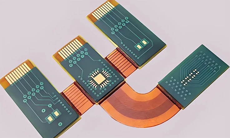
The demand for smaller, lighter, and more dynamically capable electronic products has driven the adoption of rigid-flex PCBs. Using a high-performance material like S1140F for the rigid sections brings reliability advantages but also presents unique fabrication challenges.
Engineering the Rigid-to-Flex Transition Zone
The most mechanically sensitive area in a rigid-flex design is the transition zone where the rigid material ends and the flexible section begins.
●CTE mismatch between S1140F and the polyimide core is managed through advanced stack-up modeling to minimize stress at the interface.
●A specialized “no-flow” S1140F prepreg is used to bond the rigid sections without adhesive flowing into and stiffening the flexible arms.
●Lamination profiles are precisely controlled to ensure the no-flow prepreg fully cures while preserving the flexibility of the flex sections.
Ensuring Mechanical Reliability in Dynamic Applications
The flexible portion of the board is designed to bend, and it must continue to perform as expected throughout its intended use.
●A laminated polyimide coverlay is specified for dynamic applications due to its superior durability compared to a simple flexible solder mask.
●Optimal bend radii and strain relief features (e.g., radiused corners) are incorporated into the layout to distribute mechanical stress and prevent trace cracking.
Advanced Signal Integrity Engineering
Achieving specified signal integrity levels is a primary objective. While material selection is foundational, control over the physical transmission line environment ultimately determines performance.
Impedance Control and Etch Compensation
Achieving a target impedance requires precise control over the final trace geometry.
●The chemical etching process results in a trapezoidal trace cross-section, not a perfect rectangle.
●A proprietary “etch compensation factor” is applied to the artwork in the CAM engineering process.
●This ensures the final, physical trace yields the exact specified impedance, compensating for the known etching behavior.
Return Path Management for EMI Reduction
High-frequency signals require a contiguous, low-inductance return path.
●Any discontinuity in this path (e.g., a slot or split plane) increases EMI and causes signal-degrading reflections.
●A comprehensive DFM review includes an analysis of return path integrity for all high-speed nets to identify and rectify potential issues.
Via Stub Removal through Controlled Depth Drilling (Back-drilling)
In thick multilayer boards, the unused portion of a via barrel acts as a resonant stub.
●This stub severely attenuates signals at specific frequencies, disrupting system functionality at data rates above 10-25 Gbps.
●The prescribed solution is Controlled Depth Drilling (back-drilling), a secondary drilling operation.
●This process physically removes the unused stub, resulting in a clean, high-bandwidth signal path.
Reliability Verification and Failure Analysis Protocols
A claim of “high reliability” must be substantiated by objective evidence. The manufacturing process is therefore underpinned by a regime of rigorous testing and a scientific approach to quality verification.
Thermomechanical Stress Simulation and Testing
A suite of tests is used to simulate the operational life of the PCB.
●Includes solder shock tests to simulate the intense thermal shock of assembly.
●Employs deep thermal cycle testing (e.g., -55°C to +125°C for 1000 cycles) to simulate years of operational use and test for via fatigue.
Accelerated Life Testing Methodologies (HALT & HASS)
For new product introductions, accelerated testing methods are employed.
●HALT (Highly Accelerated Life Test): A destructive test applying combined thermal and vibration stress to identify the fundamental operational limits of the design.
●HASS (Highly Accelerated Stress Screen): A non-destructive production screen using a less intense stress profile to identify units with latent manufacturing defects.
Advanced Interconnect Stress Testing (IST)
IST is an automated method for quantifying interconnect reliability.
●Provides fast, quantitative data on the board’s thermomechanical robustness.
●Works by rapidly heating a test coupon with an electrical current and continuously monitoring its resistance to detect the precise moment of via failure.
The Failure Analysis Escalation Process
In the event of a failure, a systematic root cause analysis is initiated.
●Begins with non-destructive methods like X-ray inspection.
●Escalates to destructive physical analysis, primarily microsectioning, to expose the failure site.
●Utilizes Scanning Electron Microscopy (SEM) for high-magnification imaging of anomalies.
●Employs Energy-Dispersive X-ray Spectroscopy (EDX) to determine the exact elemental composition of any defect or contaminant.
The Chain of Trust: Material Traceability in the Supply Chain
In high-reliability electronics, the integrity of the final product is a direct function of the integrity of its constituent materials. A comprehensive “Chain of Trust” is therefore established, centered on absolute material traceability and stringent supply chain control.
The Role of the Certificate of Conformance (CofC)
Every panel of Shengyi S1140F laminate received is accompanied by a Certificate of Conformance from the material supplier.
●A formal attestation that the material meets all specified properties as defined by the relevant IPC-4101 slash sheet.
●Cross-referenced with internal incoming inspection data for verification.
Implementing Lot and Batch Traceability
Upon receipt, every sheet of material is assigned a unique internal lot number, which is digitally linked to the supplier’s original batch number.
●A unique ID is tracked and logged at every key stage of the fabrication process.
●Allows for immediate isolation of any suspect material in the event of a process deviation.
●Enables the generation of a complete traceability report for the final product, linking it back to the specific raw material batch.
Proactive Counterfeit Prevention Strategies
All critical materials are procured exclusively through officially authorized and audited distributors.
●A short and tightly controlled approved vendor list is maintained.
●Baseline material analysis is performed on incoming laminates for certain programs to create a unique property “fingerprint”.
●This fingerprint serves as a reference against which future batches can be verified, allowing each run to match the original specifications precisely.
Engineering Engagement: From Concept to Fabrication
The successful realization of a complex, high-reliability PCB is the outcome of a structured, collaborative engineering process. This section outlines the typical pathway from an initial design concept to the delivery of fully qualified hardware, providing a clear framework for technical engagement.
Initial Technical Consultation and DFM Analysis
The process commences with the submission of a preliminary design package, which typically includes layout files and a proposed stack-up.
●A comprehensive Design for Manufacturability (DFM) analysis is conducted on the submitted data.
●The objective is to identify any potential fabrication challenges, opportunities for yield enhancement, or areas for cost optimization early in the design cycle.
●The output is a detailed report providing actionable feedback to the design authority.
Collaborative Stack-up Design and Impedance Modeling
Following the initial review, a collaborative effort is undertaken to finalize the board’s layer stack-up.
●Advanced field-solver software is used to model the proposed construction to precisely determine trace geometries and dielectric thicknesses.
●The goal is to finalize all material selections to meet all specified impedance targets (e.g., 50Ω single-ended, 100Ω differential pairs).
●The outcome is a locked-down, fully manufacturable stack-up diagram that serves as the definitive blueprint for the board.
Sample Impedance Calculation Parameters (Modeled in Polar Si9000e or Similar):
| Impedance Type | Trace Width (mil) | Trace Spacing (mil) | Dielectric Thickness (mil) | Target Impedance (Ω) |
| Single-Ended (50Ω) | 5.0 | — | 4.0 | 50 ±10% |
| Differential (100Ω) | 4.5 | 5.0 | 3.6 | 100 ±10% |
| Broadside Coupled | 4.0 | 4.0 | 2.5 (between planes) | 90 ±10% |
Formal Quotation and First-Article Inspection (FAI) Plan
With the technical design finalized and approved, the commercial and quality planning phase begins.
●A formal quotation is generated based on the exact material specifications, layer count, and process requirements of the design.
●A First-Article Inspection (FAI) plan is developed concurrently.
●This plan explicitly details the specific tests and analyses (e.g., microsections, TDR measurements) to be performed on the initial units to provide objective evidence of compliance.
Project Execution and Quality Data Reporting
Upon commencement, the project enters the fabrication sequence as detailed in the preceding sections.
●The culmination of the engagement is the delivery of the finished PCBs, accompanied by a comprehensive data package.
●This package typically includes full material traceability reports, Certificates of Conformance for the laminate, and the completed FAI report.
●This provides a transparent and complete quality record for the delivered hardware.
Project Realization with JarnisTech: A Commitment to Engineering Excellence
The preceding sections have detailed the complex interplay of material science, design principles, and fabrication processes required to produce high-reliability PCBs. The successful orchestration of these elements is what defines a top-tier circuit board supplier. The JarnisTech approach is founded on four pillars of engineering and operational excellence.
Mastery of Advanced Fabrication Processes
The engineering ethos at JarnisTech is centered on the deep, practical understanding of how to transform advanced materials into reliable hardware.
●Demonstrated control over the lamination process ensures the full thermomechanical benefits of low-CTE materials like S1140F are realized.
●Expertise in advanced via formation techniques, including controlled-depth drilling (back-drilling), enables next-generation signal integrity performance.
●Proven capability with complex structures, such as rigid-flex and HDI boards, allows for the realization of highly integrated, modern electronic designs.
Total Cost of Ownership (TCO) Optimization
The focus extends beyond the initial unit price to the total cost of ownership for the end customer. A higher-quality board translates to lower downstream costs.
●Reduces the risk of costly board-level failures during system integration and testing.
●Prevents latent field failures, avoiding immense warranty, recall, and reputational costs.
●Accelerates time-to-market by delivering high-yield, reliable boards that eliminate redesign cycles caused by manufacturing defects.
Agile Project Management and Predictable Timelines
In complex product development, maintaining a clear sequence of steps helps reduce uncertainty. The JarnisTech project management methodology is structured to offer clients dependable scheduling and clear visibility throughout the process.
●An intensive front-end DFM analysis minimizes surprises and delays once fabrication begins.
●A streamlined workflow and transparent communication ensure clients are informed of project status at every stage.
●The result is a disciplined execution that allows clients to maintain their own development and integration schedules with a high degree of confidence.
Dedicated Engineering Support and a Collaborative Process
The engagement model is not a simple transaction but a collaborative engineering relationship.
●Access to dedicated application engineers is provided throughout the project lifecycle.
●Support extends from initial stack-up design and material selection to final quality data interpretation.
●This collaborative approach, outlined in the preceding “Engineering Engagement” section, ensures a seamless translation of design intent into a physical, reliable product.
FAQs for Shengyi S1140F
1.What is the recommended maximum hit count for drill bits when processing S1140F?
To maintain optimal hole wall quality, a maximum hit count of 1,500-2,000 is recommended for small diameter bits (<0.5mm) before resharpening or replacement.
2.What type of routing bit provides the cleanest edge finish when depaneling S1140F boards?
A diamond-cut or chip-breaker style router bit is recommended. It provides a cleaner, smoother edge finish and reduces mechanical stress on the laminate compared to standard burr-style bits.
3.When should plasma treatment be considered as part of the S1140F fabrication process?
Plasma treatment is recommended as a desmear alternative for boards with very high aspect ratio vias (>10:1) or for critical HDI applications where ensuring pristine hole wall integrity is paramount.
4.What is the ideal copper surface treatment for inner layers to maximize bond strength with S1140F prepregs?
A multi-stage chemical oxide replacement or an alternative low-profile brown oxide process is recommended. These create a micro-roughened surface ideal for optimal resin bonding without aggressive mechanical abrasion.
5.How does S1140F behave with different types of press pads during lamination?
It performs well with standard kraft paper and conformal press pads. However, for designs with fine features, using a pressure-equalizing conformal sheet helps ensure uniform pressure and prevents localized resin starvation.


