Printed Circuit Board (PCB) Assembly is the process of mounting electronic components onto a circuit board. PCBs are used extensively in the manufacturing of electronic equipment, and their assembly involves a combination of manual and automatic processes, such as soldering, inspection, testing, and more.
It is important to note that the PCB Assembly process is separate from the manufacturing of PCBs themselves, which includes design and prototyping. The actual assembly process involves the precise placement of Active and Passive Electronic Components onto the PCB, depending on the unique characteristics of the PCB and the specific application it is intended for.
The assembly of electronic components is therefore a crucial step in the overall PCB manufacturing process, requiring skilled technicians and specialized tools in order to ensure accurate and reliable assembly. PCB Assembly Manufacturers play a key role in this process, utilizing their expertise to produce high-quality, fully functional circuit boards that meet the needs of a wide range of modern electronic devices.
Introduction to Printed Circuit Board Assembly (PCBA)
Printed Circuit Board Assembly (PCBA) is the process of assembling electronic components onto a printed circuit board (PCB) to create a functional electronic device or product. The PCB is the foundation of most electronic products and acts as a platform for the placement and interconnection of electronic components. PCBA involves a series of steps that include solder paste application, pick and place of components, reflow soldering, inspection, and testing. The PCBA process requires specialized equipment, expertise, and quality control measures to ensure that the final product meets design specifications and is reliable and safe for use. The PCBA process has evolved over the years to become more automated and efficient, with advancements in technology leading to smaller, more complex, and higher density circuit boards.
The History and Evolution of PCBA
The history of Printed Circuit Board Assembly (PCBA) can be traced back to the early 20th century when simple radio circuits were constructed on thin sheets of Bakelite or Masonite material. In the 1940s, during World War II, the use of PCBs became prominent for military applications and by the 1950s, printed circuit boards became more widely used in commercial applications. The early PCBs were single-sided and used through-hole components.
In the 1960s, the use of surface-mounted components on PCBs was introduced, which allowed for the miniaturization of electronic products. As PCB technology advanced, the use of automated assembly equipment, such as pick and place machines, and reflow soldering ovens, became more prevalent in the 1980s, leading to increased production efficiency and reduced costs.
In the 1990s, the high-density interconnection (HDI) technology was developed, which enabled the integration of more components on smaller PCBs, paving the way for smaller and more powerful electronic devices such as smartphones and tablets.
Today, the PCBA industry continues to evolve, with advancements in technology enabling even more miniaturization, enhanced functionality, and increased reliability. The use of flex PCBs, rigid-flex PCBs, and 3D printing is becoming more widespread, and the introduction of the Internet of Things (IoT) has led to higher demand for smaller and more energy-efficient PCB assemblies. The trend towards smart manufacturing and Industry 4.0 is also driving the development of more automated and connected PCBA processes.
PCB Design and Layout Considerations
PCB design and PCB layout considerations are critical in Printed Circuit Board Assembly (PCBA) as they can affect the functionality, reliability, and manufacturability of the final product. Here are some key considerations:
● Component selection and placement: The placement of components on the PCB should be optimized for the best performance, thermal management, and ease of assembly. Components should also be selected based on their availability, cost, and performance requirements.
● Signal integrity and power integrity: The PCB should be designed to ensure proper signal integrity by minimizing noise, crosstalk, and signal reflections. Proper power delivery and distribution networks are also required to ensure power integrity.
● PCB stackup and layer count: The PCB stackup should be designed to minimize noise and crosstalk while optimizing signal and power integrity. The layer count should be optimized for the complexity of the circuit and the size of the board.
● Trace routing and spacing: The routing of traces on the PCB should be designed to minimize noise and EMI issues while optimizing signal integrity. Trace spacing should also be optimized for the required conductor width, voltage, and current.
● Thermal management: The design should ensure proper heat dissipation and thermal management to prevent issues such as overheating, component failure, and signal distortion.
● Design for manufacturability (DFM): The PCB design should be optimized for ease of assembly and cost-effective manufacturing.
● PCB testing: The design should allow for proper testing of circuits and components to ensure performance and reliability.
Therefore, PCB design and layout considerations are critical in ensuring that the final PCBA product meets performance requirements, is reliable, and can be manufactured efficiently and cost-effectively.
PCB Fabrication Overview
PCB fabrication is the process of manufacturing the Printed Circuit Board (PCB) that serves as the base for Printed Circuit Board Assembly (PCBA). The PCB fabrication process involves a series of steps, including the following:
● Design: The PCB design is created using PCB design software or other CAD tools.
● Substrate material selection: The substrate material for the PCB is selected based on the requirements of the circuit. Common substrate materials include FR-4, polyimide, and Rogers laminates.
● Copper layer formation: Copper is deposited onto the substrate material through a process called electroless copper plating.
● Photolithography: A photoresist layer is applied to the copper layer, and a pattern is created with the use of a photomask. The copper layer is then etched to remove excess material using a chemical process.
● Drilling: Holes are drilled into the PCB to create the required vias and through-holes.
● Plating and solder mask application: Additional copper plating is applied to the PCB, followed by the application of a solder mask to protect the copper layers and to indicate the location of solder pads.
● Silkscreen printing: A layer of ink is applied to the board’s surface using a silkscreen process to print component labels, logos, and other markings.
● Electrical testing: The PCB is subjected to electrical testing to ensure that it meets design specifications and is free from defects.
PCB fabrication is a complex process that requires specialized equipment and expertise. The quality of the PCB is critical to the performance and reliability of the final product. Additionally, advancements in PCB fabrication technology have led to the development of new substrate materials, more precise manufacturing processes, and increased fabrication efficiency.
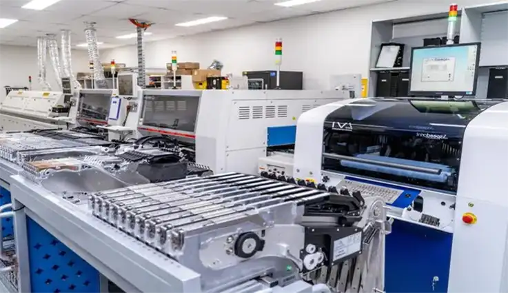
PCBA Process Flow
The PCBA process flow involves a series of steps that transform a printed circuit board (PCB) into a functional electronic device or product. The typical PCBA process flow includes the following steps:
● Solder paste application: Solder paste is applied to the PCB surface using a stencil printing process or jetting.
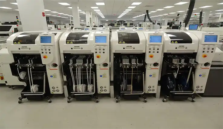
● Pick and place of components: Automated pick and place machines are used to accurately place surface mount components onto the PCB. Through-hole components are typically placed manually.
● Reflow soldering: The PCB is heated in a reflow oven to melt the solder paste, forming a permanent solder joint between the components and the PCB.
● Inspection: Quality control checks are performed to ensure correct component placement, proper soldering, and any defects are identified and addressed.
● Testing: The assembled PCB is electrically tested to ensure it meets the required performance specifications and functionality.
● Rework and repair: If any defects or issues are identified during inspection or testing, rework and repair may be required to correct them.
● Final assembly: Additional components such as connectors, cables, and housings are added to the PCB to complete the final assembly of the electronic product.
Overall, the PCBA process flow requires specialized equipment, expertise, and quality control measures to ensure that the final product is reliable, safe, and meets the required performance specifications. Additionally, advancements in PCBA technology have led to the development of more automated and efficient processes, reducing production time and costs while increasing manufacturing yield and product reliability.
How Many Methods Are Needed To Make PCB Assembly ?
There are two major techniques that a PCBA manufacturer could employ for PCB assembly:
Surface-Mount Technology
Surface-mount technology (SMT) is a sophisticated assembly process that involves mounting electronic components directly onto the surface of a printed circuit board (PCB). This method is highly automated and flexible and enables manufacturers to achieve higher connection density and greater precision in the assembly of complex circuits.
By using SMT, manufacturers have the ability to incorporate intricate circuitry into smaller components. This is made possible by the precision placement of components directly onto the surface of the PCB, which eliminates the need for bulky mounting structures. The result is a more compact and efficient electronic device with improved performance and reliability.
SMT has become increasingly popular due to its many advantages, including greater flexibility, speed, and accuracy, which allows for an improved manufacturing process and higher quality end products. Manufacturers who utilize SMT assembly methods must have the necessary expertise and specialized equipment to ensure that all components are placed in the correct location, with the correct orientation, and with the appropriate level of bonding to create a fully functional electronic device.
● The PCB Is Prepared: First, the assembler puts solder paste in the areas it’s required on the board.
● Then, The Components Are Placed: Next, the assembler puts elements on the boards, typically with a pick-and-place machine.
● Reflow Soldering: The assembler heats the boards inside an oven for reflow till the paste has reached the temperature that is required for solder joints to be formed.
● Checking: The assembler conducts inspections throughout the SMT process, which includes prior to attaching components, and prior to and following the reflow soldering process.
Through-Hole Technology
The thru-hole technique is an assembly method that involves the drilling of holes in a printed circuit board (PCB) to allow for electronic components, referred to as leads, to be inserted and connected. This technique has been around for many years and is considered an older technology in comparison to surface-mount technology (SMT). Despite this, the thru-hole technique offers unparalleled durability and reliability due to the stronger connections created between the components and the board.
In the thru-hole assembly process, leads of components are inserted into corresponding holes in the PCB and then soldered to create a strong and reliable bond. This method can also accommodate larger components compared to those used in surface-mount technology.
Even though SMT has gained more popularity in recent years, the thru-hole technique is still commonly used in certain applications, especially for components that require higher mechanical strength and stability. Manufacturers with knowledge and experience in both SMT and thru-hole assembly methods are able to provide a wide range of options to meet the varied requirements of different electronic devices.
● Drilling Holes: The initial step in the process of drilling thru holes involves drilling holes in the board. The holes should be the proper dimensions for the component leads.
● Place The Leads In The Holes: Next, the assembly worker places the leads into the holes.
● Soldering: The subsequent step of the procedure is the process of soldering. This ensures that the components are held securely in their place.
● Inspect: Throughout the process, the assembly goes through checks to ensure that the PCBA is operating as intended.
Surface Mount Technology (SMT) vs. Through Hole Technology (THT)
Surface Mount Technology (SMT) and Through Hole Technology (THT) are two common techniques used in Printed Circuit Board Assembly (PCBA) to mount electronic components onto a printed circuit board (PCB). There are some key differences between these two techniques:
● Component packaging: SMT components are typically smaller and lighter compared to THT components, as they are designed to be mounted on the surface of the PCB. THT components, on the other hand, have leads or wires that are inserted through the holes in the PCB and soldered onto the other side.
● PCB Design: THT components require larger holes in PCBs to accommodate the leads, while SMT components only require small pads on the PCB surface. This can impact PCB design, especially when it comes to high-density boards with limited space.
● Assembly process: SMT components are typically assembled using automated pick and place machines, while THT components are inserted manually or using selective wave soldering machines. SMT components can be assembled at a quicker rate due to automation, while THT components take more time for assembly.
● Reliability: SMT components have less physical contact with the PCB, resulting in potential issues with vibration and shock resistance. THT components, being fastened through the board, have more mechanical strength.
● Cost: The cost of SMT components is often lower compared to THT components because they are smaller and lighter, and require fewer materials. However, SMT assembly processes can be more expensive due to the need for pick and place machines and reflow ovens.
Generally speaking, the choice between SMT and THT largely depends on the design specifications, production quantity, and intended application of the electronic product. SMT is currently the more popular choice due to its smaller size, higher assembly speed, and lower cost. However, THT is still used for certain applications, such as in high-power or high-vibration environments where added mechanical strength is required.
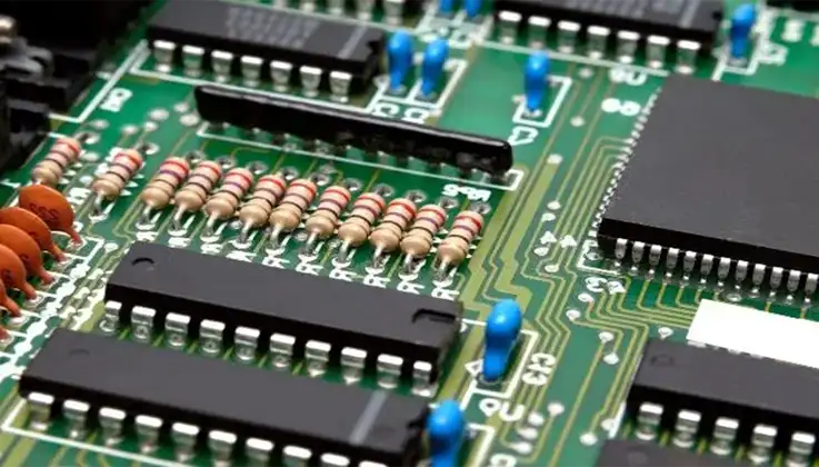
Key Components Used in PCBA
The key components used in Printed Circuit Board Assembly (PCBA) include:
● Resistors: Resistors are used to limit the flow of current in a circuit.
● Capacitors: Capacitors store and release electrical energy, stabilize power supply, and filter noise.
● Diodes: Diodes allow the flow of current in only one direction, typically used in rectification, voltage regulation, and signal processing.
● Transistors: Transistors are semiconductor devices that amplify or switch electronic signals in a circuit.
● Integrated Circuits (ICs): ICs are miniature electronic circuits that contain many electronic components such as transistors, diodes, resistors, and capacitors.
● Memory Devices: Memory Devices such as Flash memory, EEPROM, SDRAM etc. are used in electronic devices to store data and instructions.
● Microcontrollers (MCUs): MCUs are single chip microprocessors that contain all the basic components necessary for controlling a device or a system, including memory, processor, and input/output peripherals.
● Connectors and headers: Connectors and headers are used to establish electrical connections between PCBs, devices and external interfaces.
● Sensors: Sensors are used to measure physical variables such as temperature, pressure, and motion.
● Passive components: Passive components include ferrites, inductors, coils, transformers, and piezoelectric components.
The choice of components used in a PCBA largely depends on the design specifications, performance requirements, and intended application of the electronic product. Selection of the appropriate components ensures that the PCBA meets its functional and reliability requirements.
Common Challenges in PCBA and Their Solutions
There are several common challenges that can arise during Printed Circuit Board Assembly (PCBA) that can impact the functioning, reliability, and quality of the final product. Here are some of the most common challenges and their solutions:
● Component placement and alignment: Automated pick and place machines may struggle to accurately pick and place small surface mount components which can lead to incorrect placement and misalignment. Solutions include using more precise equipment, optimizing the pick and place program, using skilled operators, and implementing visual inspection systems to detect misalignment.
● Solder joint defects: Solder joint defects such as insufficient or excess solder, bridging, and voids can cause poor or inconsistent electrical connections or mechanical failures. Solutions include properly selecting the solder paste, optimizing the reflow profile, inspecting solder joints using X-ray or automated optical inspection systems, and reworking or repairing defective joints.
● Component quality issues: Poor quality, damaged, or counterfeit components can cause issues with functionality and reliability. Solutions include sourcing components from reputable suppliers, implementing quality control measures, and performing component authenticity and performance testing.
● PCB design issues: PCB design issues such as the incorrect pad size, copper trace routing, and spacing can interfere with the signal integrity, power delivery, and thermal management of the PCBA. Solutions include optimizing the PCB design using simulation and validation tools, prototype testing, and collaborating with suppliers and manufacturers for design feedback.
● Environmental factors: Environmental factors such as temperature, humidity, and the presence of dust and debris can adversely affect the performance and reliability of the PCBA. Solutions include using protective coatings, proper storage and handling procedures, and testing environmental stressors during quality control.
In summary, addressing PCBA challenges requires a combination of expertise, quality control measures, and the deployment of appropriate technology. By identifying and addressing these challenges, manufacturers can ensure the successful production of reliable, quality, and functional electronic products.
How Do Ensure PCBA Quality
In the modern era of increasingly complex and compact PCB designs, the integration of an effective Quality Assurance program throughout the assembly process is crucial to ensure the highest levels of quality and consistency. At our PCB assembly manufacturing facility, we recognize the importance of quality and have incorporated a comprehensive Quality Management System for our PCB Assembly services, which is registered to both ISO 9001:2000 and ISO/TS 16949:2002.
Our Quality Management System adheres to various strict guidelines and comprises several critical elements such as extensive design reviews, detailed documentation throughout every stage of the assembly process, advanced quality inspection and testing equipment, and highly trained quality control personnel who oversee the assembly process and ensure that quality standards are met.
As part of our Quality Management System, we consistently review our quality objectives to improve our assembly and manufacturing processes continually. Our commitment to quality is fundamental to our approach and is reflected in every aspect of our services, ensuring that our clients receive high-quality PCB products that meet or exceed their expectations.
Our quality management system for PCB Assembly services is registered to ISO 9001:2000 and ISO/TS 16949:2002. It includes the following elements:
● Functional test.
● Test the system.
● Burn-in testing.
● Environmental Stress screening.
● Visual inspections, like automated X-ray Inspection (AXI) and Automated Optical Inspection (AOI).
● Electrical testing, for example, in-circuit Testing (ICT), Flying Probe Testing (FPT) along with Boundary Scan Testing.
Quality Control and Testing Processes for PCBA
Quality control and testing are critical processes in ensuring that Printed Circuit Board Assemblies (PCBAs) are reliable, safe, and meet performance specifications. Here are some of the common quality control and testing processes used in PCBA:
● Visual inspection: Visual inspection is a basic quality control method used during the assembly process to check the placement and alignment of components, solder joints, and PCB cleanliness. Skilled operators or automated optical inspection (AOI) systems can detect faults such as missing or misaligned components, insufficient or excess solder, and surface contamination.
● X-ray inspection: X-ray inspection can be used to inspect internal solder joints and hidden component placement on the PCB. It is particularly useful in detecting issues with BGAs, QFNS, and other components that cannot be inspected by visual means.
● In-circuit testing (ICT): In-circuit testing involves checking the functionality of the assembled board by applying a series of test vectors to the board and measuring the resulting outputs to verify that the PCB has been assembled correctly.
● Functional testing: Functional testing is performed on the fully assembled product to verify that the PCBAs and mechanical components are functioning as intended in the final product. This is typically done through automated software testing, simulation, and manual test procedures.
● Environmental testing: Environmental testing involves subjecting the PCBA to various environmental stimuli like temperature and humidity, vibration, and shock to ensure that the PCBAs can withstand the expected use cases. Environmental testing can detect issues like unexpected changes in resistance, leakage currents, and other unexpected performance changes.
● Burn-In Testing: Burn-In Testing involves subjecting the PCBA to elevated stress conditions like voltage, current, temperature, and humidity to increase the chance of any latent defects coming to the surface.
By implementing quality control and testing measures at various stages of PCBA production, manufacturers can ensure that their assembled PCBs are of high quality and reliability, helping to reduce final product failure, recalls, and other issues.
How Long Does It Take to Make PCB Assembly
The duration required to complete PCB assemblies typically ranges from 7 to 20 working days and is influenced by various factors that affect the assembly time. These include:
● Manufacturing time for the PCB board: The production of bare boards must be completed before the electronic components can be assembled onto the board. This preliminary step can impact the overall assembly time.
● Quantity of PCB assemblies: The number of PCB assemblies required can also affect the time required to complete the assembly process. Larger quantities typically take longer to assemble.
● PCB IC packaging process: PCB IC packaging is typically determined by the specific application and technology required for each electronic device. Different PCB assembly methods such as SMT, BGA, through-hole assembly, QFN or mixed assembly have varying requirements and the time required for each method can differ.
● Component procurement: Sourcing and purchasing electronic components for PCBA orders can be complex. The required components may not always be available in the factory inventory and thus have to be ordered, leading to potential delays in the assembly process.
The procedure Of PCB Assembly Can Be Described As Is Described:
● PCB board manufacturing: 3-15 working days
● Procurement of BOM: related components in 17 days after receiving the order
● Circuit board assembly: 13 working days;
● Delivery and package : 1 working day before the deadline;
Most often, PCB assembly partners split the assembly order into OPL orders and non-OPL.
● OPL Purchase Order:For our inventory of components, we have the electronic components that are required to fulfill the order. This means that the costs of buying components are reduced as well as OPL orders are carried out more quickly and within a range that is manageable.
● Non-OPL Orders: Indicates that certain components of the PCB design aren’t included in our library of components. Component procurement must be completed simultaneously with the PCB board itself in order to speed up the process.
Our PCB Assembly manufacturing facility has established an efficient and streamlined production process to minimize the time required for each assembly step. Our experienced team works to ensure that every project is delivered within the specified time frame without compromising on quality or performance.
Future Developments and Advancements in PCBA Technology
The ongoing technological advances in Printed Circuit Board Assembly (PCBA) technology are enabling higher performance, more efficient, and cost-effective electronic products. Here are some of the future developments and advancements that are expected in PCBA technology:
● Advanced materials: The development of new materials like nanotechnology-based materials and composites is expected to enhance the thermal management, electrical conductivity, and mechanical stability of PCBs.
● Miniaturization: PCBs with higher component density, smaller sizes, and faster speeds are being designed and targeted to facilitate the development of next-generation electronic products. This is enabled by the development of new manufacturing techniques, including HDI, microvia, and embedded component technology.
● 5G Applications: With 5G technology’s mass adoption, PCBAs will need higher bandwidths to support increased data rates, lower latencies, and other 5G benefits.
● IoT Integration: PCBAs must be designed to support a range of wireless protocols including Bluetooth, WLAN, RFID, and IoT protocols such as Zigbee for the integration of IoT functionalities.
● Advanced Automation: The development of advanced robotics, pick-and-place machines, and other automated systems are expected to increase speed, productivity, and precision, while reducing production time and cost.
● Additive manufacturing: The advancements in 3D printing and additive manufacturing are being applied to fabricating both PCBs and electronic components.
● Green Technology: Environmentally friendly and energy-efficient PCB materials and manufacturing processes are being developed.
Constant developments and research in PCBA technology are expected to help in the production of smaller, faster, more efficient, and more reliable electronic products. These innovations can lead to a significant impact in enabling emerging technologies like autonomous vehicles, smart homes, and smart cities in the near future.
PCBA Professionals
JarnisTech stands out as the premier supplier of PCB solutions. Whether you require parts sourcing or electronic assembly, we are fully equipped to meet your PCB needs. Our commitment to providing a comprehensive manufacturing experience and maintaining strict quality control ensures that we support you every step of the way.
Choosing JarnisTech as your trusted PCBA partner means gaining access to superior quality products and services. Our PCB assembly services conform to the highest standards, including IPC Class 3 RoHS and ISO certification. This allows us to efficiently handle any type of PCB, whether single-sided or double-sided, with SMT through-hole or mixed-assembly configurations. We thrive on delivering tailored solutions that meet your specific requirements.
As your project progresses, JarnisTech maintains constant communication with you, optimizing production processes, reducing wait times, and improving overall product quality to save you time and money on PCB costs. Our goal is to support you, allowing you to focus on your PCB designs without worrying about the profound details of manufacturing
Related Posts:
- Mixed PCB Assembly Technology Services For Your Next New Project
- Why Electronic Potting is So Important in PCB Assembly?
- A Full Guide to Electro mechanical Assemblies
- Cable and Wire Harness Assembly
- Electronics Components PCB Assembly
- China:The Best PCB Consignment Assembly Services At JarnisTech
- PCB Box Build Assembly
- Nine Method of Save Cost PCB Assembly Production
- How Many Types of Turnkey PCB Assembly?