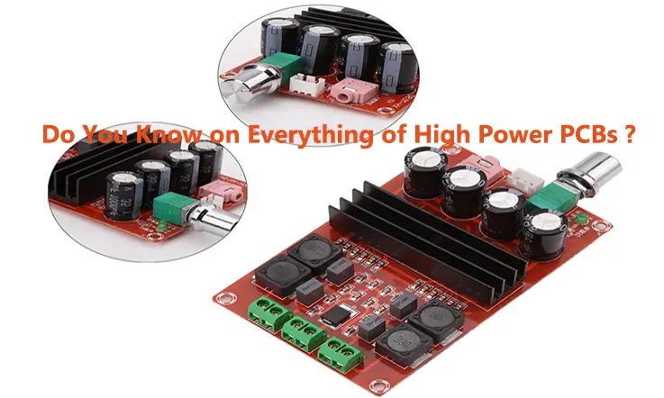
High power PCBs are designed to handle high currents, thermal stress, and demanding structural requirements. Their development involves careful attention to factors such as thermal management, material selection, stack-up structure, and EMI control. This article provides an in-depth look at design strategies and manufacturing processes, including copper thickness optimization, multilayer assembly, and thermal simulation. It also covers emerging technologies like SiC/GaN integration and AI-based layout analysis. Each section offers clear, practical information tailored to industry needs.
Understanding High Power PCBs
High Power PCBs are engineered to withstand electrical loads that exceed standard PCB ratings. These boards are specifically crafted with thick copper laminates, tailored dielectric materials, and heat-dissipating configurations to manage increased current flow and voltage. Their structural makeup supports stable electrical transmission without compromising mechanical integrity or thermal stability. They are widely incorporated in systems where consistent performance and reliable energy distribution are required.
Designing High Power PCBs involves deeper considerations beyond ordinary trace routing or pad sizing. It calls for a closer look into copper weight, thermal vias, and substrate conductivity. Factors like temperature resistance, current carrying capacity, and controlled impedance are routinely taken into account.
What Is a High Power PCB and How Does It Function?
A High Power PCB refers to a printed circuit board designed to carry and manage high current and voltage levels. These boards typically feature enhanced copper thickness — often 2 oz or more — and utilize base materials that offer favorable thermal transfer characteristics.
Conductive layers are purpose-built to support increased amperage without excessive thermal buildup. High Power PCB manufacturing also requires tight process control in layer stacking, copper plating, and final inspection. Features such as plated through-holes, wide traces, and reinforced edge plating further define their mechanical resilience.
Their function hinges on minimizing energy loss, keeping internal resistance under check, and maintaining stable temperature across operational cycles. High Power PCB design also includes robust grounding and effective EMI shielding to ensure clean signal routing and noise mitigation.
Power Density, Current Ratings, and Voltage Handling Explained
High Power PCBs are typically characterized by their ability to sustain higher-than-average electrical parameters:
●Power Density: Directly tied to board size and current handling, this aspect reflects how much power is distributed over a unit area.
●Current Ratings: Determined by copper thickness, trace width, and board layer configuration. Wider traces and heavier copper reduce resistive heating.
●Voltage Handling: Defined by creepage and clearance distances, the dielectric strength of materials, and proper insulation planning.
These characteristics are integral to High Power PCB design. Understanding the interplay of these elements helps avoid heat concentration, dielectric breakdown, and unplanned shutdowns in field applications.
High Power PCB laminates must be chosen with surface temperature, expansion coefficients, and dielectric properties in mind. The fabrication process also adjusts according to the thermal expansion characteristics of the laminate to prevent layer separation or crack propagation over long-term use.
Industries That Rely on High Power PCBs (EV, Solar, Telecom, Medical)
Many industries integrate High Power PCBs into their systems, often to manage electrical efficiency, compact system footprints, and consistent thermal profiles. These include:
●Electric Vehicles (EVs): Applications such as onboard chargers, traction inverters, and battery interface circuits depend on solid High Power PCB design and manufacturing processes.
●Renewable Energy Systems: Solar and wind infrastructure utilize High Power PCBs to regulate high-voltage DC-AC conversion and manage load balancing between sources and grids.
●Telecommunications Infrastructure: Power amplifier boards, RF distribution units, and base stations integrate these boards for consistent signal and power distribution.
●Medical Devices: Imaging systems and diagnostic equipment implement High Power PCB materials to support high-load electronics with reduced thermal stress.
●Heavy Industrial Equipment: Robotics, drive controllers, and automated machinery employ these boards to maintain functional continuity and electrical regulation under operational strain.
Across all sectors, High Power PCB types — from metal-core and ceramic substrates to multi-layer high current boards — are engineered with reliability, long-term usage, and electrical tolerance in mind. Their grounding techniques, trace routing, and thermal management strategies are optimized for system-level integration.
High Power PCB Types: From Metal Core to Flexible and Rigid-Flex
Selecting the right type of high power PCB structure involves a combination of thermal considerations, mechanical constraints, current load demands, and product lifecycle requirements. Applications ranging from automotive onboard chargers to telecom base stations and solar inverters each demand a different mechanical and electrical configuration. This section explores how rigid, metal core PCB, hybrid PCB, and flex-rigid boards compare in design use cases, and what factors influence material choice when addressing current density, heat transfer, and structural durability.
Comparison of Rigid, MCPCB, Hybrid, and Flex Power Boards
Each PCB type provides a different approach to managing power, heat, and structural integration. Understanding these options allows for tailored electrical performance and mechanical fit across sectors.
●Rigid High Power PCBs:
— Typically constructed with multiple layers of FR4 or polyimide.
— Support high copper weights (up to 10 oz) for industrial-grade power delivery.
— Common in converters, control systems, and static power electronics.
●Metal Core PCBs (MCPCBs):
— Include aluminum or copper substrates for improved thermal conduction.
— Direct thermal path reduces the need for additional heat sinks.
— Often used in LED lighting arrays, power drivers, and battery management systems.
●Hybrid PCBs:
— Combine FR4 with metal substrates or embedded ceramics.
— Allow for localized heat spread while maintaining standard routing layers.
— Applied in areas where both signal integrity and thermal performance are required.
●Flexible and Rigid-Flex PCBs:
— Use polyimide-based substrates for bendable interconnects.
— Reduce space requirements in folded or compact assemblies.
— Deployed in electric vehicles, robotics, and portable energy storage.
This table provides a direct comparison of structure and application focus:
| PCB Type | Thermal Path | Typical Current Load | Mechanical Profile | Application Focus |
| Rigid | Through via & planes | Medium to High | Stiff, layered | Inverters, rectifiers, servers |
| MCPCB | Direct to metal core | High | Rigid metal-backed | LEDs, drivers, high wattage LEDs |
| Hybrid | Mixed layer systems | Variable | Mixed stiffness | Telecom, industrial automation |
| Flex / Rigid-Flex | Thin polyimide films | Low to Medium | Flexible or foldable | EV battery modules, sensors |
Application-Specific Types: Automotive, Inverters, Chargers, UPS
Matching PCB structure to application isn’t just about form factor—it also involves current-carrying demands, heat management strategy, and operational environment.
●Automotive Power Boards:
— Typically rigid or rigid-flex.
— Built for sustained vibration, thermal cycles, and current surges.
— Used in DC-DC converters, onboard chargers, and traction inverters.
●Inverters and Solar Converters:
— Often based on MCPCB or heavy copper rigid boards.
— Emphasize planar heat dissipation and high isolation ratings.
— Capable of handling grid-tied or battery-linked conversion loads.
●EV Chargers (AC & DC Fast Charging):
— Use mixed materials including thick copper and metal-core layers.
— Designed to manage 400V to 800V input ranges.
— Include reinforced insulation and spacing for creepage control.
●UPS and Industrial Backup Systems:
— Generally multilayer rigid boards with high dielectric strength.
— Must remain stable during load transitions and battery switching.
— Thermal fatigue resistance is a main performance metric.
Each use case is bound by material, electrical, and environmental parameters—choosing the right combination enhances system lifespan and compliance with regulatory benchmarks.
Mechanical Strength, Thermal Paths, and Flex Durability
Beyond electrical considerations, the physical properties of high power PCBs often dictate final design suitability. Material selection and layout directly influence both durability and thermal behavior.
●Mechanical Reinforcement:
— Stiffeners and thick copper layers improve board rigidity and mechanical shock resistance.
— Metal core boards resist deformation under thermal load cycles.
●Thermal Path Engineering:
— Thermal vias, copper planes, and direct-contact base metals are employed for heat routing.
— Interface materials (TIMs) are used to couple the PCB to external heatsinks.
●Flexing and Dynamic Bending Performance:
— Rigid-flex circuits are tested for repeated bending cycles.
— Polyimide-based substrates maintain dielectric stability at elevated temperatures.
— Copper routing requires controlled bending radius to avoid cracking or fatigue.
A multi-physics approach—addressing electrical, thermal, and mechanical behavior simultaneously—provides the foundation for robust high power PCB selection and layout.
High Power PCB Design Fundamentals: Current Flow, Layout & Thermal Optimization
When dealing with high current and elevated thermal demands, High Power PCB design requires more than generic layout rules. Proper trace geometry, material selection, and thermal distribution strategies are fundamental to ensuring reliable electrical performance over time. This section provides a detailed view of current flow dynamics, layout best practices, and thermal regulation in high power circuit board configurations.
Trace Width Calculations, Ampacity, and Voltage Drop Mitigation
Every High Power PCB must support efficient current transmission without exceeding thermal boundaries. A precise understanding of trace dimensions and current load ratings helps maintain performance and prevent failure.
●Trace width should be calculated using IPC-2152 guidelines, taking into account copper thickness (e.g., 2 oz, 3 oz), ambient temperature, and board stack-up.
●Ampacity requirements change with trace location—external layers dissipate heat more effectively than internal ones.
●Voltage drop becomes more pronounced across long power distribution paths. Wider traces and shorter routing distances can help maintain consistent voltage levels.
●Thermal rise should remain within the limits defined by the substrate material and copper laminate type used.
●Current-carrying optimization involves distributing power through parallel traces or copper pours to reduce localized heating.
High Power PCB Layout Tips: Grounding, Via Design, and Parasitics
A well-structured layout plays a defining role in mitigating thermal stress and suppressing electrical noise. Ground structure, via strategy, and parasitic management all contribute to the board’s overall reliability.
●Ground plane continuity helps reduce EMI and stabilize reference points. A split ground can be applied when analog and power sections must be isolated.
●Thermal vias placed beneath heat-dissipating components like MOSFETs or IGBTs allow effective heat transfer to inner or bottom copper layers.
●Via size and count must align with current density and thermal load. For example, a high-current path may require several 0.3 mm vias per amp of current.
●Parasitic inductance is minimized through compact trace geometry and minimized loop areas in high-frequency paths.
●Copper pour zones around sensitive circuitry should be isolated from high power nodes to prevent unintended coupling.
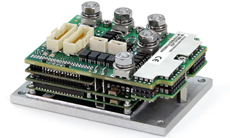
Integrating Power Components: MOSFETs, IGBTs, and Heat Sources
High power components are thermal hotspots. Their placement and integration must support efficient heat extraction and minimal interference with other circuitry.
●MOSFETs and IGBTs should be mounted on heat-spreading areas, such as thick copper zones or direct-to-metal substrates.
●Component spacing should allow for airflow (natural or forced) and thermal isolation from heat-sensitive devices.
●Thermal pads with vias connecting to large copper planes improve dissipation while maintaining electrical integrity.
●Substrate selection matters—using materials like FR-4 with high Tg or advanced laminates like Rogers or polyimide supports long-term performance at higher operating temperatures.
●Heat spreaders or heatsinks may be attached to high power areas depending on the power density and available cooling method.
Advanced Thermal Management Techniques for High Power PCBs
When dealing with high current applications such as inverters, energy storage systems, or EV charging equipment, managing heat is part of ensuring operational consistency. Heat doesn’t just dissipate — it needs engineered routing, materials that can handle the load, and modeling that ensures nothing is left to chance. This section outlines three practical domains: how heat is evacuated, how its behavior is predicted, and how materials support the system under stress.
Heat Dissipation Mechanisms: Thermal Vias, Copper Planes, Heat Sinks
Thermal pathways help manage the buildup caused by resistive losses and high-frequency switching components. These techniques are widely adopted across high power PCB manufacturing setups, especially where MOSFETs, IGBTs, and DC-DC converters are used.
●Thermal vias connect surface components to inner copper layers or metal backings. They are often grouped in dense arrays beneath heat-generating parts to draw heat downward.
●Copper planes, both on outer and inner layers, spread localized heat horizontally. Wider areas help maintain temperature gradients across the board.
●Heat sinks provide external support by drawing thermal energy out via direct contact with component packages or mounting holes. They’re typically paired with thermal interface materials for maximum transfer.
●Metal core PCBs (MCPCBs) — especially aluminum-based — combine internal heat spreaders with outer sink contact points to minimize the need for bulky cooling systems.
●Thermal pads and heat-spreading films are used where direct sink mounting is not possible. These materials often bridge the gap between surface-mounted devices and metal layers underneath.
This layered approach makes thermal management scalable depending on power density and board footprint.
Thermal Simulation and CAD Modeling Best Practices
Before committing to production, simulation helps forecast how the PCB handles thermal stress over time. This is especially useful in high power PCB design where design margins are tighter.
●CAD-based simulation tools such as Altium, SolidWorks PCB, and ANSYS allow layout-driven heat profiling under specific load conditions. These tools simulate power dissipation, airflow, and thermal resistance.
●Thermal maps highlight hot spots and help refine copper area, trace placement, and component orientation. Adjustments in via density or copper thickness can be evaluated before fabrication.
●Transient thermal analysis is used in systems where the load isn’t constant — such as inverter drives or battery management PCBs — to observe thermal cycling behavior.
●Comparative testing post-simulation is often done using IR thermography or embedded thermal sensors to verify CAD predictions. These tests are aligned with IPC-2152 standards to validate real-world performance.
Simulation enables iterative refinement and can help reduce failure rates due to thermal fatigue or delamination.
PCB Material Selection for High Temperature Performance
Material selection isn’t just about Tg ratings — it involves thermal conductivity, expansion behavior, and compatibility with multi-layer builds. Choosing the right substrate is a common discussion point during early-stage high power PCB manufacturing planning.
●High-Tg FR-4 is widely used due to its balance between cost and thermal performance. Variants rated at ≥170°C are common in telecom power units and high-density LED drivers.
●Polyimide laminates maintain structural integrity under elevated temperature cycles and are favored for aerospace or industrial motor drive PCBs.
●Metal core PCBs (aluminum or copper-based) improve conduction from top-layer components into the core, effectively reducing hotspot formation.
●Ceramic-filled hydrocarbon and PTFE materials offer consistent dielectric performance with increased thermal resilience, suitable for RF power circuits or compact converters.
●Hybrid stack-ups are sometimes used in mixed-voltage applications, combining FR-4 layers with thermal interface prepregs or backing metals.
| Material Type | Tg (°C) | Thermal Conductivity (W/m·K) | Application Area |
| High-Tg FR-4 | ≥170 | ~0.3 | Consumer power supply, chargers |
| Polyimide | ~200 | ~0.4 | Industrial, aerospace power circuits |
| Aluminum MCPCB | 130–150 | 1.0–3.0 | LED drivers, power modules |
| Ceramic-filled PTFE | ~200 | >1.5 | RF power boards, base stations |
The thermal integrity of the final PCB is highly dependent on how materials interact with copper layouts and operating cycles.
Grounding and EMI Control Techniques in High Power PCB Design
High power PCB systems often operate with rapidly switching currents and substantial voltage swings, both of which contribute to unwanted electromagnetic interference (EMI). This interference can affect not only the board itself but also surrounding systems and communication interfaces. Grounding and EMI mitigation aren’t just about following design “rules”—they involve a comprehensive understanding of current return paths, impedance matching, and spatial geometry across planes and layers. From star grounding schemes to shielding strategies and careful signal routing, the choices made during layout heavily influence the overall electromagnetic performance of the product.
Star Grounding, Return Path Design, and Power/GND Planes
Ground configuration directly influences noise coupling, common-mode currents, and potential oscillations. Establishing clean return paths and proper plane segmentation helps ensure current flows predictably without generating unintentional radiators.
●Star Grounding Strategy:
— Keeps analog, digital, and power returns separate until a defined single-point connection.
— Reduces loop areas by preventing cross-domain noise interference.
— Applied especially in mixed-signal power designs.
●Return Path Considerations:
— High-frequency return currents follow the path of least impedance, not shortest distance.
— Plane integrity below signal traces ensures minimal loop inductance.
— Discontinuities in ground or power planes may introduce unintended radiators.
●Power and Ground Plane Management:
— Solid copper fills offer low impedance return paths.
— Planes should be tightly coupled to reduce parasitic inductance.
— Split planes must include controlled stitching capacitance to suppress resonance.
| Element | Application Note | EMI Benefit |
| Star Grounding | Central return hub for power and control domains | Limits ground bounce and noise loops |
| Solid GND Plane | Under all signal and power paths | Creates uniform return path impedance |
| Plane Stitching | Capacitive vias or resistive bridges | Equalizes voltage across split regions |
Shielding, Filtering, and Signal Integrity in High Current Systems
The combination of filtering components and physical layout techniques plays a central role in suppressing emissions and protecting signal integrity. High current paths must be managed alongside high-speed signals without introducing cross-domain interference.
●Shielding Approaches:
— Grounded copper pour around high-speed nets reduces radiated EMI.
— Enclosures and metal cans should be connected to low-impedance ground points.
— Grounded via fences can isolate aggressive nodes.
●Input/Output Filtering:
— LC filters reduce conducted EMI at connector interfaces.
— Common-mode chokes remove noise on balanced lines.
— Ferrite beads block high-frequency harmonics without affecting DC load paths.
●Signal Integrity Maintenance:
— Controlled impedance routing is essential for differential pairs and clock lines.
— Avoid routing sensitive signals near high-current power traces.
— Layer stackup should preserve consistent impedance and minimize skew.
PCB Layout Guidelines to Minimize EMI and Crosstalk
Proper physical design plays a preventive role in EMI management. Layer ordering, trace geometry, and isolation techniques all contribute to lower emissions and better system compliance with regulatory requirements.
●Trace Spacing and Routing:
— Keep high-speed signal lines short and away from switching power traces.
— Use 45° angles instead of 90° bends to reduce reflection points.
— Route differential pairs in parallel and maintain constant spacing.
●Via and Plane Considerations:
— Minimize the number of vias in high-speed paths to reduce inductive discontinuities.
— Use via stitching around high-speed and noisy areas for shielding.
— Decoupling capacitors must be placed as close as possible to IC power pins.
●Layer Stack Optimization:
— Place high-speed signals between two ground planes (stripline) to minimize EMI.
— Ensure that adjacent power and ground planes are tightly coupled to control impedance.
— Use dedicated return layers for high-speed nets when possible.
Here’s a quick comparison table highlighting layout tactics:
| Layout Feature | Functionality | EMI/Crosstalk Impact |
| 45° Routing | Smooth signal transitions | Reduces signal reflections |
| Via Stitching | Ground continuity around noise sources | Contains radiated EMI |
| Controlled Impedance | Consistent trace width & dielectric | Preserves signal shape and timing |
| Power-GND Plane Coupling | Low loop inductance | Suppresses common-mode noise |
High Power PCB Materials and Laminates: Choosing the Right Stackup
In high-power applications, such as power converters, electric vehicle control systems, and industrial drives, the selection of PCB materials directly influences thermal management, electrical performance, and mechanical stability. Different materials have distinct properties in terms of thermal conductivity, dielectric strength, glass transition temperature (Tg), and coefficient of thermal expansion (CTE). This section will delve into the performance of materials like FR4, polyimide, and metal-core boards, helping you choose the right stack-up for your specific application.
FR4 vs Polyimide vs Metal-Core Boards for Thermal Conductivity
Thermal conductivity is a core parameter when evaluating PCB materials for high-power applications. Below is a comparison of the thermal conductivity of common materials:
| Material Type | Thermal Conductivity (W/m·K) |
| FR4 | 0.25 – 0.35 |
| Polyimide | 0.2 – 0.3 |
| Metal-Core (Aluminum) | 120 – 180 |
| Copper | 385 – 400 |
●FR4: Widely used in various electronics, FR4 is cost-effective but has relatively low thermal conductivity, often requiring additional thermal management measures, such as thermal vias and heat sinks.
●Polyimide: Known for its excellent thermal stability and mechanical strength, polyimide is used in high-temperature environments but offers thermal conductivity similar to FR4.
●Metal-Core Boards (MCPCB): By incorporating a metal core—typically aluminum or copper—MCPCBs enhance thermal conductivity to a considerable degree. This makes them well-suited for applications that demand effective heat dissipation, such as high-power LED lighting and power conversion modules.
Dielectric Strength, Tg, and Thermal Expansion Coefficient Explained
In high-power PCB design, dielectric strength, glass transition temperature (Tg), and the coefficient of thermal expansion (CTE) directly affect how materials handle electrical loads and thermal cycling.
| Material Type | Tg (°C) | Dielectric Strength (MV/m) | CTE (ppm/°C) |
| FR4 | 130–180 | 20 | 10–20 |
| Polyimide | 200–260 | 20–25 | 20–30 |
| Metal-Core (Aluminum) | 150–180 | 25–30 | 23 |
●Dielectric Strength: This refers to the maximum electric field a material can withstand before electrical breakdown occurs. Materials with higher dielectric strength are better suited for high-voltage applications.
●Glass Transition Temperature (Tg): Tg represents the temperature at which a material transitions from a rigid, glass-like state to a more flexible, rubber-like state. Materials with higher Tg provide better dimensional stability at elevated temperatures.
●Coefficient of Thermal Expansion (CTE): CTE defines the rate at which a material expands as temperature increases. Matching the CTE of materials helps reduce thermal stress, which can prevent damage to solder joints and vias.
High Power PCB Laminates for High Voltage and Heat Resilience
Under high-voltage and high-temperature conditions, selecting a suitable laminate stack-up influences electrical reliability and thermal endurance. Below is a breakdown of commonly used laminate structures:
●FR4 Laminates: Suitable for medium power and temperature applications, offering good mechanical properties and cost-efficiency.
●Polyimide Laminates: Well-suited for high-temperature and high-voltage environments thanks to strong thermal stability and reliable dielectric properties.
●Metal-Core Laminates (MCPCB): Incorporating a metal core significantly improves thermal conductivity, making them well-suited for high-power LED lighting and power modules that require efficient heat dissipation.
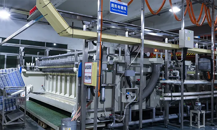
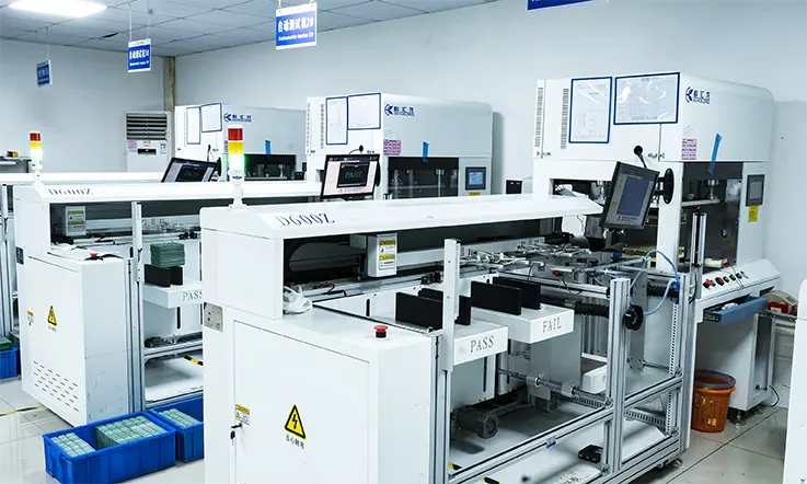
High Power PCB Manufacturing: Processes, Standards, and Quality Control
Manufacturing high power PCBs demands close coordination among process engineering, material selection, and thermal management. Applications such as EV charging stations, telecom base stations, and solar inverters rely on PCBs that maintain uniform copper distribution, withstand thermal stress, and deliver stable electrical performance. This section outlines techniques for handling heavy copper fabrication, constructing dependable multilayer stack-ups for power transmission, and applying IPC standards to ensure consistency and verification throughout production.
Heavy Copper Manufacturing Techniques and Etching Considerations
Heavy copper techniques are applied when circuits must carry higher currents or handle greater thermal demands than standard PCBs allow.
●Copper thickness levels: Boards may carry copper weights from 2 oz/ft² up to 20 oz/ft², depending on the application. Designs with current paths above 40A typically require 4 oz or thicker copper.
●Controlled etching: Thicker copper requires adjusted etching profiles to manage sidewall definition and undercut prevention. Without proper control, etch geometry can deviate, reducing trace reliability.
●Pattern plating: Often used for localized copper build-up, pattern plating allows designers to reinforce specific areas without affecting the entire layer.
●Cleaning protocols: Post-etch cleaning eliminates residues that can affect adhesion or introduce contamination during multilayer lamination.
For high power PCB manufacturing, copper thickness directly impacts current-carrying capacity, while etch uniformity ensures predictable performance under thermal stress.
Multilayer Stack-Up Strategies for High Current Applications
Multilayer stack-ups distribute power, control heat buildup, and reduce electromagnetic interference through careful layer arrangement and material choices.
●Symmetry and balance: Balanced stack-ups help prevent warpage during lamination and reflow. Symmetrical copper distribution is especially helpful for boards with high copper weight.
●Insulating layer placement: Choosing the correct dielectric materials and positioning them between copper layers reduces the risk of electrical breakdown.
●Prepreg selection: High resin content prepregs are often required to fill heavy copper areas and prevent voiding during lamination.
●Sequential lamination: For complex boards, building layers in stages allows for better control of pressure, flow, and resin curing.
High current applications demand stack-ups that manage not just power flow, but also mechanical alignment and thermal expansion over repeated load cycles.
IPC Standards, Testing, and Thermal Stress Verification
Reliable high power PCB fabrication is tied to process control, material traceability, and compliance with industry guidelines. IPC standards support these needs by defining measurable quality benchmarks.
●IPC-6012 Class 2 and Class 3: These classes define different inspection levels for conductivity, thermal cycling, and layer alignment. Class 3 is typically used for industrial-grade or mission-dependent applications.
●Thermal cycling tests: Boards are exposed to environmental extremes such as -55°C to +125°C over hundreds of cycles to verify layer adhesion and material stability.
●Electrical integrity tests: Automated test fixtures or flying probe systems are used to detect shorts, opens, or insulation breakdown.
●CTE matching analysis: Coefficient of thermal expansion differences between copper, laminate, and plating materials are measured to reduce the chance of cracking or delamination.
●Solderability and stress testing: Solder pads and vias are tested for wettability and resilience under load or temperature variation.
Design for Manufacturability (DFM) in High Power PCB Assembly
High power PCBs must be designed not only for electrical and thermal performance, but also with fabrication and assembly efficiency in mind. Without proper attention to DFM principles, even a well-performing layout can face production delays, rework cycles, or increased cost per unit. In high-current environments, DFM goes beyond simple clearance rules—it requires thorough planning for thermal zoning, stress reduction during soldering, and maintaining panel-level structural integrity. By anticipating mechanical and assembly constraints early, a layout can transition more predictably from CAD to volume production.
Component Placement and Thermal Zone Optimization
Component layout directly influences heat concentration, assembly flow, and rework accessibility. Dense areas around high-power devices can create bottlenecks during reflow, while uneven thermal distribution may distort solder joints or stress vias.
Thermal Zoning Practices-
●Group heat-generating parts in a shared zone to balance reflow profiles.
●Separate sensitive analog or timing circuits from heat-heavy power components.
●Align thermally demanding regions with dedicated copper pours or metal-core areas.
Placement Strategy-
●Maintain uniform spacing between large packages to avoid shadowing during soldering.
●Avoid placing tall components near connectors or test points.
●Place temperature-sensitive devices away from heat sources and copper pour transitions.
Manufacturing Example-
●In a 6-layer 48V inverter control board, misaligned FETs created uneven soldering across zones. Adjusting pad sizes and spacing along with targeted pre-bake stages reduced X-out rates by 17%.
| Layout Factor | Assembly Outcome | Mitigation Approach |
| Dense Thermal Cluster | Localized warping during reflow | Thermal balancing via copper redistribution |
| Asymmetric Layout | Differential heat soak and tombstoning | Align components along thermal symmetry lines |
| High Pin Count ICs | Solder voids in power pads | Stencil design adjustments and vacuum reflow |
Solder Joint Integrity and Assembly Line Constraints
The performance of high power PCBs depends heavily on consistent solder joints, especially in high current and thermal cycling environments. Material expansion, surface finish compatibility, and line-level process limitations all play into joint quality.
Solder Pad and Land Pattern Design-
●Use IPC-7351-compliant footprints with appropriate toe, heel, and side spacing.
●Thermal relief in power planes should be balanced to avoid cold joints.
●Avoid large thermal mass copper pads without heat sinking vias or aperture control.
Assembly Process Considerations-
●Reflow profiles must be tailored to match thermal mass variation across the panel.
●Excessive copper can delay solder melt or create voids under thermal pads.
●Surface finishes (OSP, ENIG, ImmSn) must align with storage and flux chemistry.
Practical Tip:
During dual-sided assembly, heavy components on side A may need mechanical support during side B reflow to prevent joint cracking or tilt. Reversible fixtures or glue dots can help hold parts in place.
| Joint Defect Type | Common Cause | Suggested Action |
| Voiding | Large copper area under pads | Use via-in-pad with controlled resin fill |
| Cold Joints | Uneven heating in multi-zone ovens | Adjust reflow ramp-up and soak times |
| Tombstoning | Asymmetrical thermal loading on resistors | Modify land sizes and equalize heat sinking paths |
Managing Warpage, Tolerances, and Panel Stack Stability
Thermomechanical deformation during assembly can affect coplanarity, break tooling, or reduce solder joint yield. Warpage is especially problematic in boards with high copper content and uneven dielectric distribution.
Panel Design Factors-
●Use symmetrical stack-ups across top and bottom layers to minimize internal stresses.
●Avoid over-routing on one side which can disrupt material balance.
●Maintain copper distribution between power and ground layers within ±10%.
Manufacturing Constraints-
●FR4 and hybrid boards exhibit varying warpage thresholds; 0.75% bow/twist tolerance is standard (IPC-6012).
●Thicker PCBs (2.0mm and up) are more stable but harder to process with laser cut or depanelization.
●Multilayer builds require adhesive compatibility to avoid delamination during thermal cycling.
Control Strategies-
●Bake panels before assembly to reduce outgassing and moisture expansion.
●Include breakaway tabs and tooling holes for better handling during pick-and-place.
●Use thieving patterns to normalize copper distribution in low-density areas.
| Factor | Common Issue | Recommended Tactic |
| Stackup Asymmetry | Warping during reflow | Mirror copper weights on opposing layers |
| Panel Moisture | Blistering or delamination | Controlled bake at 120°C for 2–4 hours before use |
| Tolerance Drift | Misalignment in automated depanelization | Use fiducials and tighter registration controls |
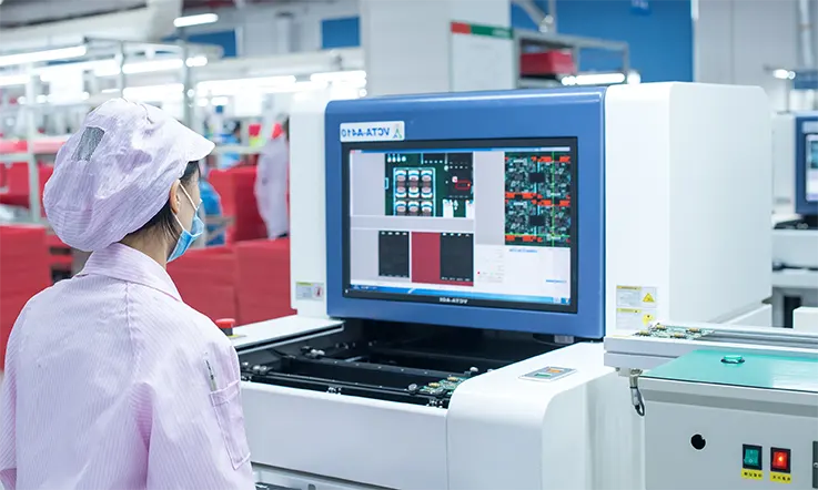
Inspection, Testing, and Failure Analysis of High Power PCBs
High power printed circuit boards must undergo rigorous testing and inspection procedures to validate their electrical, thermal, and mechanical performance before deployment in high-current or high-voltage systems. These procedures not only help ensure conformance to manufacturing specifications but also assist in identifying early degradation patterns and possible weak points under real-world operating conditions. The selection and combination of test methods often depend on board complexity, layer count, conductor thickness, and application-specific loading requirements.
AOI, X-ray, Flying Probe, and Functional Load Testing
The effectiveness of post-manufacturing inspection processes relies on a mix of non-destructive and electrical testing methodologies tailored to high copper weight and multilayer stack-ups. Typical inspection and testing practices include:
●AOI (Automated Optical Inspection): Detects surface-level solder bridges, tombstoning, component misalignment, and pad defects. Particularly useful for early-stage identification in SMD assembly lines.
●X-ray Inspection (AXI): Penetrates dense copper layers to reveal internal defects such as voids under BGAs, cold solder joints, and barrel cracks.
●Flying Probe Testing: Enables net-to-net electrical verification without requiring a fixture, suitable for prototyping and low-volume production runs.
●Functional Load Testing: Simulates real operational load conditions to validate voltage tolerance, temperature rise, and power conversion accuracy under stress.
These tools complement each other and, when used in sequence, provide comprehensive feedback for both production calibration and ongoing quality monitoring.
Common Failure Modes: Delamination, Overheating, Copper Cracking
Identifying recurring failure patterns helps establish root causes and refine upstream design rules and process controls. Common high power PCB failure modes include:
●Delamination: Often caused by moisture entrapment, improper lamination pressure, or uneven curing, resulting in layer separation under thermal cycling.
●Overheating Damage: Triggered by insufficient thermal relief or under-engineered heat dissipation paths, leading to discoloration, substrate brittleness, or melting.
●Copper Trace Cracking: Frequently occurs in heavy copper designs when subjected to repeated thermal or mechanical strain. Cracks typically form near vias, bends, or corners.
Failure analysis using cross-sectioning, infrared thermography, and SEM (scanning electron microscopy) helps pinpoint precise failure origins and validate mitigation strategies.
Reliability Testing: Thermal Shock, Burn-in, and HALT
Reliability evaluation under controlled but aggressive test cycles helps verify long-term endurance across thermal, mechanical, and electrical domains. Common reliability test protocols include:
●Thermal Shock: Cycles the PCB between extreme temperature highs and lows to expose CTE mismatches and solder fatigue risks.
●Burn-In Testing: Subjects the assembly to sustained electrical and thermal load over extended periods, highlighting weak interconnects and overstressed passive components.
●HALT (Highly Accelerated Life Testing): Applies simultaneous thermal, vibration, and electrical stress beyond rated limits to uncover premature failure paths.
| Test Type | Target Defect Mechanism | Duration | Typical Use Case |
| Thermal Shock | Delamination, Pad Lift | 100–1,000 cycles | High-temp environments |
| Burn-In | Early electrical failure | 24–168 hrs | Power modules, converters |
| HALT | Mixed stress interactions | Short bursts | Prototyping reliability |
Future Trends in High Power PCB Technology
This section explores forward-facing technologies reshaping high power PCB design, fabrication, and integration. From SiC and GaN advancements to predictive AI modeling and multifunctional embedded systems, these technologies are not just enhancements—they’re directional shifts in thermal management, power density handling, and intelligent control. By incorporating performance-driven semiconductor platforms and embedded sensing, high power PCBs are advancing toward greater compactness and thermal resilience, particularly under high-switching frequency and high-voltage stress conditions. Read on for detailed comparisons, design data points, and implementation insights.
SiC and GaN Integration in High Voltage Applications
Wide bandgap materials such as Silicon Carbide (SiC) and Gallium Nitride (GaN) are reshaping the voltage and switching frequency thresholds in power systems. Unlike traditional silicon, these materials enable higher breakdown voltages and faster switching speeds, which leads to reduced conduction and switching losses.
●Thermal conductivity and switching frequency: SiC supports higher junction temperatures compared to silicon, which enables more compact component arrangements. GaN enables high-frequency operation, which helps reduce the need for extensive EMI filtering.
●Layout considerations: High dV/dt and dI/dt transients from GaN devices require tight coupling between power and ground loops to mitigate overshoot and ringing.
●Die attach and substrate compatibility: Direct bonded copper (DBC) and active metal brazed (AMB) substrates are increasingly adopted to support thermal paths compatible with WBG thermal behavior.
Example: A 650V GaN half-bridge circuit implemented on a 4-layer PCB using ENEPIG finish showed 40% less EMI compared to traditional silicon equivalents, when the power loop area was minimized below 3 cm².
AI-Based Thermal Design and Simulation
Modern PCB development integrates machine learning algorithms for thermal and electrical simulation to accelerate optimization cycles and reduce trial-and-error during prototyping.
●Pattern recognition: AI can predict hotspot formation by analyzing trace routing and component clustering across thousands of design iterations.
●Data-driven parameter tuning: Algorithms adjust copper thickness, via density, and pad geometries based on heat flux trends in high-density areas.
●Co-simulation workflows: Integration with SPICE, CFD, and ECAD platforms enables real-time parametric sweeps across power profiles and ambient conditions.
Example Table: AI Simulation Outputs vs Traditional Iteration
| Simulation Method | Design Cycle Time | Peak Temp Accuracy | Iteration Count |
| Manual Optimization | 8 Weeks | ±7°C | 12 |
| AI-Augmented Modeling | 3 Weeks | ±2.5°C | 3 |
Smart PCBs, Sensor-Integrated Boards, and IoT Power Modules
As monitoring and predictive maintenance take center stage in power systems, high power PCBs are evolving to include sensing and communication functionality within the substrate itself.
●Integrated sensors: Temperature, current, and voltage sensors embedded into the PCB layers offer real-time telemetry for load forecasting.
●Modular power interfaces: IoT-connected DC-DC converters and battery management circuits now use standardized pads and plug-in headers for field upgrades.
●System-level fault tracing: Onboard diagnostics log transient events such as voltage dips, arc flashes, or sudden impedance shifts for later review.
Example Use Case: An industrial UPS unit with sensor-embedded power PCBs enabled real-time reporting of inverter stage degradation via an MQTT gateway, reducing service response time by 60%.
FAQ & High Power PCBs
1. What defines a PCB as “high power”?
A PCB is considered high power when it handles high current (typically above 5A) and requires enhanced thermal management.
2. Can high power PCBs use standard FR4 material?
Standard FR4 can be used in low to moderate power designs, but alternatives like polyimide or metal-core are preferred for better thermal performance.
3. What is the impact of high current on PCB via reliability?
High current increases via temperature; thus, via diameter, quantity, and plating thickness must be optimized to avoid failure.
4. How do high power PCBs handle transient power surges?
Designs often include snubbers, clamping diodes, or embedded protection circuits to manage power spikes.
5. Is it possible to include controlled impedance in high power PCBs?
Yes, but impedance control must be balanced with thermal and current-carrying constraints.
6. What is the typical operating temperature range for high power PCBs?
Most high power PCBs are designed to operate between -40°C and 125°C or higher, depending on materials.
7. Can flex circuits be used in high power applications?
Yes, in specific cases where moderate current and dynamic bending are required, often with reinforced copper and stiffeners.
Related Posts:
1.Everything to Know about Inverter PCB Why So Important
2.High Voltage PCBs: Design, Manufacturing, Assembly and Industry Standards