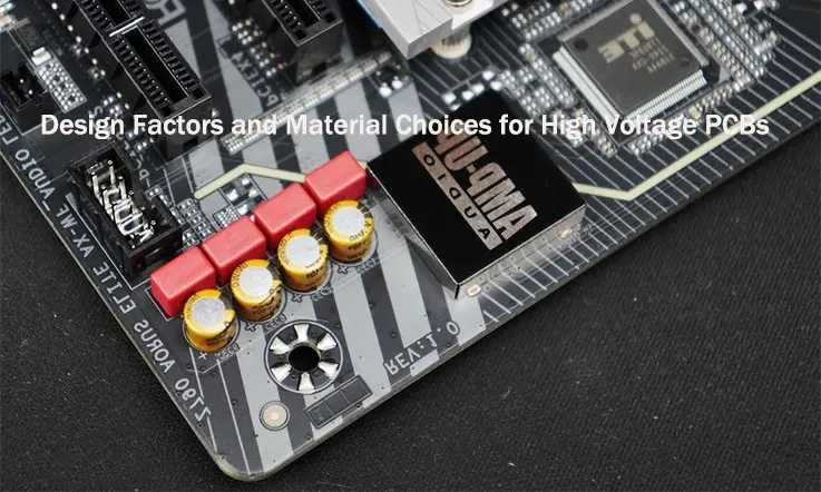
High Voltage Printed Circuit Boards (PCBs) are widely used in sectors that require high electrical power and reliability, including renewable energy, electric vehicles, and power electronics. These PCBs are specifically designed to handle higher voltages and current levels, while ensuring electrical safety and long-lasting performance. With technological progress and the increasing need for reliable, high-performance systems, the demand for High Voltage PCBs continues to grow. These PCBs help meet the challenges of powering next-generation electric vehicles and supporting critical renewable energy systems.
This guide dives deep into the critical aspects of High Voltage PCB design, manufacturing, assembly, and the latest industry standards. We will explore key factors like dielectric strength, thermal management, and compliance with electrical safety standards, which are crucial for ensuring the performance and reliability of these PCBs. Furthermore, we’ll discuss how new material innovations and emerging technologies are driving the evolution of high voltage designs.
Why Should You Design PCBs for Systems of High Voltage?
One primary reason for the widespread use of printed circuit boards capable of handling high voltages is their necessity in various industries. Sectors such as high voltage applications, power generation, military, and aerospace heavily rely on these specialized boards. Utilizing alternative PCBs in these industries can lead to increased arcing, which not only incurs substantial costs but also causes significant inconvenience.
Benefits of a High Voltage PCB Design
There are numerous benefits associated with high voltage PCB designs, primarily attributed to the utilization of heavier copper compared to other PCB designs. These advantages include enhanced endurance against thermal strains, ensuring that the board can effectively withstand thermal fluctuations.
Moreover, high voltage PCBs exhibit increased current-carrying capacity, a characteristic not commonly found in other types of boards. Additionally, these boards offer superior mechanical strength, particularly evident in plated-through holes (PTH) and connector sites. By incorporating a higher copper weight on the circuitry layer, high voltage PCBs enable a significant reduction in the overall product size. Furthermore, copper-plated vias facilitate efficient heat transfer to external heatsinks, optimizing thermal management.
Drawbacks of a High Voltage PCB Design
However, high voltage PCB designs do come with certain challenges. One of the main challenges is the higher cost. Using thicker copper for better conductivity adds to material costs, which increases overall production expenses. Additionally, the fabrication and assembly of high voltage PCBs generally take longer than standard PCBs. The extra steps required, such as the use of heavier copper and other specific design modifications, extend the production timeline.
The widespread use of high voltage PCBs across different industries is largely due to their ability to manage high voltages effectively. These specialized boards provide several advantages, including better resistance to thermal stress, higher current-carrying capacity, and greater mechanical strength. However, there are also some challenges to consider, such as higher costs and longer production times. Even with these considerations, high voltage PCBs continue to be indispensable in sectors where consistent performance under high voltage conditions is needed.
Introduction to High Voltage PCBs
High Voltage PCBs are a specialized category of PCBs designed to handle voltages far higher than those found in standard PCBs, often exceeding 100V and reaching several kilovolts in certain cases. These boards are widely used in industries where power conversion and control are essential, including power electronics, renewable energy systems, and electric vehicles (EVs). The growing need for compact, reliable, and efficient high-voltage components in advanced technologies underscores the role these PCBs play in driving modern engineering solutions.
In high voltage PCB design, considerations extend far beyond traditional circuit board layouts. These boards are specifically tailored to handle electrical isolation, thermal stress, and high voltage levels without compromising performance. With that in mind, let’s take a closer look at what makes high voltage PCBs different, how they are used in various applications, and the factors that go into their design.
What Are High Voltage PCBs and Their Key Characteristics?
High Voltage PCBs are designed to manage electrical voltages beyond the capabilities of standard PCBs. These specialized boards are commonly used in applications that demand both high power handling and effective electrical isolation, where precise engineering is necessary to maintain stable and consistent performance.
Here are some of the characteristics that set high voltage PCBs apart:
1.PCB Materials: The materials used in high voltage PCBs need to withstand high voltages without breaking down. Materials like ceramic, PTFE (polytetrafluoroethylene), and FR4 are commonly chosen for their dielectric strength and reliability under extreme conditions. These materials allow the PCB to maintain structural integrity even in high-stress environments.
2.Breakdown Voltage: The breakdown voltage is the maximum voltage at which the insulating material on a PCB will fail. High voltage PCBs are designed with careful attention to trace width, spacing, and material selection to ensure that the breakdown voltage comfortably exceeds the operating voltage. Proper spacing between traces and components helps to prevent electrical failure and maintain reliable operation under high voltage conditions.
3.Dielectric Strength: Dielectric strength refers to the ability of the PCB material to resist electrical breakdown under high voltage. High voltage PCBs rely on materials with excellent dielectric properties, such as ceramic or PTFE, which help prevent arcing and leakage currents. The higher the dielectric strength, the better the material can withstand electrical stress.
For high voltage PCB our designers, understanding these materials and properties is core to ensuring both the safety and efficiency of their designs. You can think of it like building a high wall that holds back a flood—if you use the right materials and build it to the right specifications, it won’t buckle under pressure.
Applications of High Voltage PCBs in Modern Electronics
High Voltage PCBs are essential in a wide variety of applications across industries that deal with substantial electrical currents. These applications often require unique materials and design specifications to maintain system performance under high voltage conditions. Here’s how high voltage PCBs fit into some of the most modern electronics:
1.Power Electronics: Power electronics are devices designed to manage the flow of electrical energy efficiently, often converting it between different forms. High voltage PCBs are used in inverters, DC-DC converters, and power amplifiers, where they facilitate energy conversion while maintaining reliable performance and thermal management.
●Example: In a solar inverter, high voltage PCBs are responsible for converting the direct current (DC) from solar panels into alternating current (AC) for residential or industrial use. The PCB must manage high currents while keeping electrical isolation intact.
2.Renewable Energy: With the global push toward clean energy, high voltage PCBs are a core part of systems used in wind turbines, solar power arrays, and battery storage systems. These PCBs ensure that electrical conversion and distribution are efficient, helping renewable energy systems meet modern demands.
●Example: Wind turbine controllers rely on high voltage PCBs to manage the electrical output from the turbine and ensure safe power conversion to the grid.
3.Electric Vehicles (EVs): As the electric vehicle industry grows, the need for high voltage PCBs has soared. These PCBs are integral in battery management systems (BMS), on-board chargers (OBC), and powertrain electronics. They ensure the efficient transfer of energy while ensuring insulation and thermal control.
●Example: High voltage PCBs in electric vehicle battery packs help manage charging and discharging cycles, keeping the system stable and balanced.
The Role of High Voltage PCBs in Safety and Performance
In high voltage applications, ensuring the safety and efficiency of electrical systems is non-negotiable. The design of high voltage PCBs requires a strategic approach to prevent electrical hazards, control heat, and manage power delivery across sensitive circuits. Let’s explore how these boards contribute to maintaining both safety and performance.
1.Electrical Safety: Ensuring electrical safety in high voltage systems is all about insulation and separation between high voltage components and lower voltage parts of the system. High voltage PCBs are designed with specific trace widths, component placements, and spacing to guarantee that electrical currents do not flow where they shouldn’t, preventing short circuits or arcing.
●Example: In industrial power systems, a high voltage PCB may feature a combination of wide traces and robust insulation materials to protect both the user and equipment from electrical faults.
2.Thermal Management: High voltage circuits often generate substantial heat, which can damage components and affect performance if not properly managed. High voltage PCBs incorporate thermal vias, heat sinks, and material selections that help dissipate heat effectively.
●Example: Power inverters used in industrial applications rely on high voltage PCBs that are equipped with thermal management systems to keep components within safe temperature ranges, avoiding overheating or system failure.
3.High Voltage Circuit Design: The design of high voltage PCBs requires careful balancing of several factors, such as the trace width, spacing, and the materials used. This precise design work ensures that the board can handle the electrical stresses it will face without suffering from breakdowns or other failures.
●Example: A DC-DC converter used in solar power systems uses specific trace and spacing designs to manage the electrical flow and ensure that the components function correctly without overheating or risking electrical damage.
Key Design Principles for High Voltage PCBs
Designing High Voltage PCBs involves a careful balance between safety and functionality. These boards have to handle much more than just electrical signals—they must manage the flow of high voltage currents safely and efficiently. To achieve this, we must consider multiple factors ranging from trace spacing to dielectric materials. So, what makes a good high voltage PCB design? Let’s break it down.
Design Considerations for High Voltage PCBs: Safety and Functionality
When designing high voltage PCBs, it’s essential to focus on the safety and functionality aspects of the design. This involves a detailed assessment of factors like trace spacing and breakdown voltage. These elements ensure that the board handles electrical stresses appropriately while maintaining overall performance.
1.Trace Spacing: The spacing between traces is a main factor in high voltage PCB design. If traces are placed too close together, the risk of electrical breakdown rises.. Proper spacing can prevent arcing and ensure the board operates as expected under high voltage conditions. The required spacing depends on the operational voltage and dielectric material used.
2.Breakdown Voltage: Every PCB material has a maximum voltage tolerance, or breakdown voltage. Selecting the right material, such as ceramic or PTFE (polytetrafluoroethylene), is necessary to ensure that the PCB can withstand high voltage without failure.
| Voltage Level (V) | Minimum Trace Spacing (mm) | Dielectric Material | Breakdown Voltage (V) |
| 100 | 0.5 | FR4 | 1500 |
| 500 | 1.5 | PTFE | 6000 |
| 1000 | 3.0 | Ceramic | 10000 |
Key Factors Affecting High Voltage PCB Performance
The performance of high voltage PCBs is influenced by multiple factors. These include the choice of dielectric materials, trace width, power distribution, and electrical isolation. All of these elements work together to ensure that the board can handle high current and voltage levels without failure.
1.Dielectric Materials: The materials used for insulation must have high dielectric strength to prevent current leakage and breakdown. Common choices include ceramic and PTFE, which offer excellent electrical properties under stress.
2.Trace Width: The trace width determines the amount of current a trace can safely handle. It needs to be calculated carefully to avoid overheating and ensure adequate power distribution.
| Material | Dielectric Strength (kV/mm) | Maximum Operating Voltage (V) | Trace Width (mm) |
| Ceramic | 20 | 5000 | 1.2 |
| PTFE | 15 | 6000 | 1.5 |
| FR4 | 8 | 1000 | 2.0 |
3.Power Distribution: High voltage PCBs often require careful power distribution management to avoid overloading certain areas of the board. Designing with power planes and multi-layer constructions ensures that the power is spread evenly across the circuit.
| Component Type | Power Requirement (W) | Required Trace Width (mm) |
| Power Transistor | 50 | 1.5 |
| Capacitor | 20 | 0.8 |
| Voltage Regulator | 10 | 1.0 |
4.Electrical Isolation: Ensuring proper electrical isolation between high voltage and low voltage sections of the PCB is essential. The design must make sure that power traces remain separated from sensitive signal traces to avoid interference.
Thermal Management in High Voltage PCB Design
Managing heat is an integral part of designing high voltage PCBs, especially when the board is subjected to high currents and high power levels. Therefore, poor thermal management can result in overheating and failure, so it’s necessary to design boards that effectively dissipate heat.
1.Thermal Properties: The materials used in high voltage PCB construction must have good thermal conductivity to transfer heat away from sensitive components. Copper, ceramic, and aluminum-based substrates are some of the best options for high heat dissipation.
2.Heat Dissipation: Thermal vias and heat sinks are commonly used to manage the heat generated by high power levels. Heat dissipation ensures that the PCB operates within safe temperature ranges, preventing thermal failure.
| Material Type | Thermal Conductivity (W/m·K) | Recommended Use |
| Copper | 400 | Power traces, heat sinks |
| Ceramic | 10 | High voltage insulation |
| Aluminum | 205 | Power distribution layers |
3.PCB Materials for Heat Management: Different materials offer varying degrees of thermal resistance. Ceramic substrates, for instance, not only provide excellent electrical isolation but also possess superior thermal conductivity, making them reliable for high power designs.
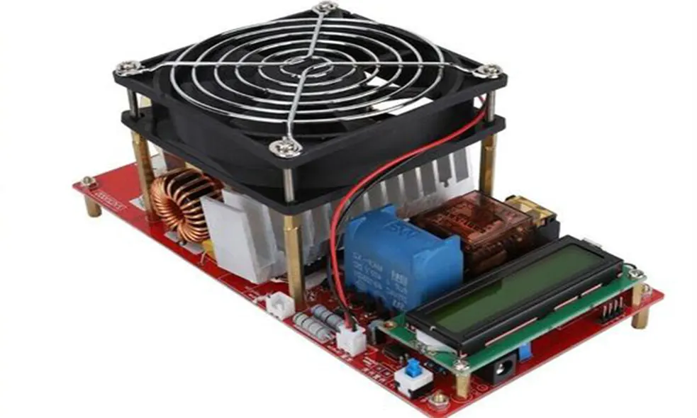
Manufacturing and Assembly of High Voltage PCBs
When it comes to high voltage PCBs, the manufacturing and assembly process requires precision and attention to detail. A simple oversight can lead to electrical breakdowns, safety hazards, or suboptimal performance. This section walks you through the high voltage PCB manufacturing process, the assembly challenges, and some of the advanced techniques used to meet the exacting demands of high voltage applications. Let’s break it down.
The Manufacturing Process for High Voltage PCBs
High Voltage PCB Manufacturing is a precise and multi-step process that involves selecting the right materials, designing with high voltage requirements in mind, and ensuring thorough electrical testing for performance and reliability. Here’s a look at what goes into the process:
1.PCB Fabrication: The first step involves creating the base structure for the PCB. This includes applying multiple layers of dielectric materials (like ceramic or PTFE) and copper traces. These materials are must to need in ensuring the PCB can handle the electrical and thermal stresses in high voltage environments. The fabrication process uses high precision to ensure the correct trace widths and spacing.
2.Dielectric Layers: High voltage PCBs rely on thick dielectric layers to separate conductive traces. Materials such as ceramic or high-temperature laminates are commonly used for these layers to ensure dielectric strength and prevent electrical breakdowns.
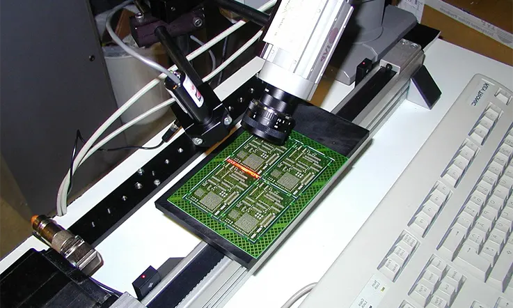
3.Electrical Testing: After the initial fabrication, the PCB undergoes rigorous electrical testing to ensure it meets the required breakdown voltage. Tests like high-voltage insulation tests and dielectric strength measurements are conducted to ensure that the PCB can handle its operating voltage without fail.
| Test Type | Voltage Level (V) | Expected Result |
| Dielectric Strength Test | 3000 | No breakdown of insulation |
| High-Voltage Test | 5000 | No leakage or failure |
| Leakage Test | 1000 | Zero current leakage |
Assembly Challenges in High Voltage PCB Manufacturing
While the fabrication process plays a large part in the overall design, the assembly of high voltage PCBs introduces its own set of challenges. From component placement to conformal coating, these PCBs require a tailored approach to ensure both electrical and mechanical dependability.
1.Component Placement: For high voltage PCBs, component placement is not as straightforward as in low voltage designs. High voltage parts need to be carefully positioned to prevent arcing and to allow for sufficient clearance between components. The placement is designed to ensure optimal insulation and protection from electrical faults.
2.Conformal Coating: High voltage circuits often require conformal coating to protect the PCB from environmental factors, such as moisture and contaminants. This protective layer is applied over the high-voltage traces to increase the PCB’s resistance to electrical breakdown and improve the board’s overall durability.
3.Voltage Tolerance: Ensuring that all components used in high voltage assemblies can handle the required voltage tolerance is necessary.. The assembly must be tested to make sure that all components can safely function at the expected operating voltages without breaking down.
| Component Type | Voltage Rating (V) | Tolerance Level | Use Case |
| Ceramic Capacitors | 5000 | ±5% | High-voltage filtering |
| Power Transistors | 2000 | ±3% | High-voltage switching |
| Resistors | 1000 | ±10% | Current limiting in power circuits |
Advanced Manufacturing Techniques for High Voltage PCBs
To meet the demands of modern high voltage applications, many manufacturers are adopting advanced techniques to ensure power distribution is as efficient and safe as possible. In this section, we explore custom PCB solutions, advanced manufacturing methods, and strategies to ensure high voltage tolerance.
1.Custom PCB Solutions: High voltage designs often require custom solutions, tailored to the specific needs of the project. Custom PCB layouts, power planes, and multi-layer constructions are frequently used to ensure that the power distribution across the board is efficient and safe. These solutions offer flexibility and durability while reducing the risk of electrical failure.
2.High Voltage Tolerance: To improve the voltage tolerance of a PCB, we can use advanced materials and techniques, such as high-temperature laminates and ceramic-filled substrates. These materials provide enhanced resistance to electrical breakdown and ensure that the board remains stable under high voltage conditions.
3.Power Distribution: Managing the flow of power across the PCB is one of the most complex aspects of high voltage design. Special attention is given to trace width, thermal vias, and multiple layers to ensure the power is evenly distributed and the PCB is capable of handling high current without overheating.
| Manufacturing Technique | Voltage Tolerance (V) | Application | Benefits |
| Custom Multi-layer PCBs | 5000 | High voltage circuits | Improved power distribution |
| Ceramic-Filled Substrates | 10000 | Power supplies | Increased dielectric strength |
| High-Temperature Laminates | 8000 | High-power systems | Enhanced heat resistance |
Industry Standards and Compliance for High Voltage PCBs
High voltage PCBs are an integral part of numerous electronic systems, ranging from industrial machinery to consumer electronics. To ensure that these boards function as expected while also adhering to the highest standards of safety and performance, we must comply with various international standards and certifications. In this section, we will explore the key global certification requirements, the compliance testing necessary for high voltage PCB design, and the specific safety standards that must be met in the industry.
Global Certification and Standards for High Voltage PCBs
When designing and manufacturing high voltage PCBs, following global standards is essential. Standards like UL Certification, IEC Standards, and IPC Standards ensure that the PCB meets safety and breakdown voltage requirements, offering assurance that the products are safe for use in demanding applications.
1.UL Certification: Underwriters Laboratories (UL) is one of the most respected organizations for testing and certification in the electronics industry. A UL Certified PCB means the product has undergone rigorous testing to ensure it meets specific electrical safety standards, including voltage tolerance and thermal performance. For high voltage applications, UL’s standards ensure that the PCB will function safely under extreme conditions, including both surge voltage and operating voltage.
2.IEC Standards: The International Electrotechnical Commission (IEC) sets global standards for electrical safety and voltage breakdown across various industries. IEC standards such as IEC 61010 and IEC 60204 provide detailed guidelines on the electrical performance and safety requirements for PCBs used in industrial settings. These standards dictate everything from component insulation to trace width and spacing.
3.IPC Standards: IPC is a global trade association that develops industry standards for PCB manufacturing and assembly. Their standards (like IPC-2221 for design and IPC-6012 for testing) ensure consistency in PCB quality, particularly in high voltage applications. These standards specify requirements for material properties, dielectric strength, and voltage endurance, ensuring that high voltage boards are reliable and safe.
| Standard Organization | Certification Type | Relevant Standards | Application Area |
| UL | UL Certification | UL 94, UL 746C | Consumer electronics, power supplies |
| IEC | International Standard | IEC 61010, IEC 60204 | Industrial equipment, machinery |
| IPC | Design & Testing Standards | IPC-2221, IPC-6012 | PCB design, manufacturing |
Compliance Testing and Regulations for High Voltage PCB Design
Compliance testing is a first step in high voltage PCB design. It’s a thorough process aimed at ensuring that every high voltage PCB meets the relevant electrical safety standards and performs reliably under real-world conditions. From breakdown voltage testing to electrical stress testing, these tests help ensure that the design will stand up to the demands of its specific application.
1.Compliance Testing: The primary goal of compliance testing is to check if the high voltage PCB meets safety regulations such as electrical insulation, breakdown voltage resistance, and thermal performance. Breakdown voltage tests, for example, measure the maximum voltage the PCB can safely handle before insulation failure occurs.
2.Electrical Safety Standards: There are strict guidelines that govern electrical safety for high voltage systems. Testing protocols assess the ability of the PCB material (such as FR4 or ceramic composites) to resist electrical breakdown under high voltage conditions. Test procedures like high-pot testing and hipot testing simulate real-world electrical stresses to verify the board’s safety under voltage surges.
3.Testing Regulations: High voltage PCB testing follows international standards like IEC 60364 (electrical installations in buildings) and UL 746 (standard for plastic materials). These regulations ensure that high voltage circuits and devices maintain electrical integrity and safety performance.
| Testing Protocol | Test Description | Standard Applied | Voltage Rating |
| Breakdown Voltage Test | Measures insulation resistance and failure point | IEC 60364, UL 746 | Up to 5000V |
| Hipot Testing | High-voltage dielectric strength testing | IEC 60204, UL 94 | 1000V to 8000V |
| High-pot Testing | Measures ability to withstand voltage without failure | UL 746, IPC-2221 | 3000V to 5000V |
Key Factors to Consider for High Voltage PCB Safety
Designing for safety in high voltage PCBs is non-negotiable. The specific nature of high voltage circuits requires careful attention to factors such as electrical arcing, reliability of components, and strict adherence to safety standards to ensure that the PCB functions as expected without risk of failure.
1.High Voltage Circuit Design: Designing circuits for high voltage applications requires precision to avoid issues like electrical arcing. The layout should minimize trace length and ensure that traces are placed with adequate spacing to prevent unintended electrical contact. Thick copper traces are used to handle high current, while sufficient insulation between traces ensures that voltage breakdown does not occur.
2.Electrical Arcing: Electrical arcing is a potential hazard in high voltage PCBs, where voltage surges can cause a breakdown of air or insulation, leading to arcing between conductors. Proper component placement and adequate clearance between traces can reduce the risk of arcing.
3.PCB Reliability and Safety Standards: Reliability is another factor in high voltage PCB design. Using materials with high dielectric strength and ensuring that all components are rated for the required voltages can significantly reduce the risk of failure. Adhering to standards such as IPC-2221 ensures that the design process integrates critical safety features, such as thermal dissipation and electrical isolation.
| Design Factor | Description | Safety Standard | Target Measurement |
| Trace Spacing | Minimum spacing between high voltage traces to prevent arcing | IPC-2221, UL 746 | 0.5mm to 2mm |
| Dielectric Strength | Resistance of PCB materials to electrical breakdown | IEC 60364, UL 746 | >20 kV/mm |
| Component Placement | Proper distance between high voltage components to prevent electrical arcing | IPC-2221 | >1.5mm clearance |
Testing and Reliability for High Voltage PCBs
In the design and manufacturing of high-voltage PCBs, testing and reliability are integral aspects. High-voltage PCBs must not only meet safety standards but also ensure long-term stability and durability in real-world applications. Various testing protocols, including high voltage testing, long-term reliability testing, and stress testing, help ensure that these PCBs perform consistently under demanding conditions. In this section, we’ll delve into the main aspects of high voltage testing, reliability testing, and stress testing to help you understand how to ensure the safety and stability of high-voltage PCBs.
High Voltage Testing Protocols for PCBs
When manufacturing and applying high voltage PCBs, following stringent testing protocols is a must. These include breakdown voltage testing and electrical testing, which help confirm the voltage tolerance and electrical insulation properties of the PCBs. These tests ensure the boards can function reliably in real-world applications, reducing the risk of electrical failure and damage.
1.High Voltage Testing: This initial test evaluates the safety and electrical performance of high-voltage PCBs under high voltage conditions. The test typically involves applying a voltage higher than the PCB’s operational voltage to ensure its electrical insulation is intact. During this process, the PCB must withstand the applied voltage without electrical breakdown, ensuring it can handle real-world electrical stress.
2.Breakdown Voltage Testing: This specific test simulates extreme operating conditions, ensuring the PCB material’s dielectric strength can withstand high-voltage stress. The PCB undergoes a voltage surge to confirm that the insulation does not fail and cause electrical shorts or failures in the circuit.
3.Electrical Testing Protocols: Several standards, such as IEC 60204, UL 746, and IPC-2221, are followed during electrical testing. These protocols ensure that the PCB’s electrical properties meet international safety and stability standards, confirming that the design can be safely used in high-voltage applications.
| Test Type | Test Description | Relevant Standard | Target Voltage Range |
| Breakdown Voltage Test | Measures the maximum voltage the PCB can withstand before breakdown | IEC 60204, UL 746 | Up to 5000V |
| Dielectric Strength Test | Tests the PCB’s insulation strength against voltage surges | IEC 60364, UL 94 | 1000V to 8000V |
| Electrical Testing | General electrical performance tests for the PCB | IPC-2221, IEC 60204 | 3000V to 10000V |
Long-Term Reliability Testing for High Voltage PCBs
It’s not enough for high voltage PCBs to pass initial tests—they must also undergo long-term reliability testing to ensure that they continue to function properly over time. These tests help identify potential issues such as material degradation or thermal failure, enabling us to address these concerns before they result in catastrophic failure.
1.Thermal Cycling Test: High-voltage PCBs experience repeated thermal expansion and contraction during operation. Thermal cycling tests simulate extreme temperature changes, ensuring that the PCB can maintain its electrical stability and physical integrity over time. These tests help assess whether the PCB can withstand the stress of heating and cooling cycles that may occur in real-world use.
2.Humidity Testing: High humidity can lead to electrical breakdown or corrosion, impacting PCB performance. Testing PCBs in various humidity conditions ensures they maintain electrical insulation and avoid short circuits or failure. These tests help determine how well the PCB performs under challenging environmental factors.
3.Insulation Resistance Testing: This test focuses on assessing the long-term performance of the PCB’s insulating materials. It checks whether the PCB’s insulation remains intact over time, even under prolonged exposure to environmental stressors. A significant part of this testing is to ensure that insulation resistance remains within safe limits, preventing breakdowns and failures.
| Test Type | Test Description | Standard Applied | Target Measurement |
| Thermal Cycling Test | Simulates temperature fluctuations and the resulting effects on PCB performance | IEC 60364, UL 746 | -40°C to 150°C |
| Humidity Testing | Tests PCB performance in varying humidity levels | IEC 60204, IPC-2221 | 95% RH at 40°C |
| Insulation Resistance Test | Measures the long-term insulation stability of the PCB | IEC 60364, UL 746 | >100 MΩ |
Stress Testing for High Voltage PCB Durability
Stress testing assesses the durability of high-voltage PCBs under extreme conditions. By simulating electrical overloads and voltage surges, stress testing helps evaluate the performance of the PCB under these high-stress scenarios. These tests not only provide valuable insight into the PCB’s ability to withstand stress but also help us identify potential failure modes and ensure the PCB’s long-term stability.
1.Stress Testing: The goal of stress testing is to simulate the electrical stress that the PCB might face in high-voltage environments. These tests help determine how well the PCB handles voltage spikes and other irregular electrical conditions that can occur during its use in actual devices.
2.PCB Durability Testing: This type of test evaluates how the PCB performs after extended periods of stress. It aims to uncover failure points that might not be immediately obvious, such as solder joint fatigue or material degradation. By subjecting the PCB to high-voltage stress and environmental factors, we can ensure that the PCB remains functional and reliable over time.
3.Failure Mode Testing: In failure mode testing, we can simulate various faults, such as electrical short circuits or burnouts, to understand how the PCB reacts under these extreme conditions. The insights gained during these tests provide crucial feedback that helps refine designs and improve the durability of the PCB in future iterations.
| Test Type | Test Description | Test Standard | Target Condition |
| Stress Testing | Simulates extreme electrical stress on the PCB | IPC-2221 | Overvoltage, Surge |
| PCB Durability Test | Evaluates long-term durability of PCB materials under high voltage | UL 746, IEC 60204 | >1000V for 5000 hours |
| Failure Mode Testing | Simulates various PCB failure scenarios | IPC-2221 | Overload, Short Circuits |
Emerging Technologies in High Voltage PCB Design
High voltage PCB design is undergoing a significant transformation as new technologies gain traction in the industry. Several innovations are improving the efficiency and performance of high voltage systems. Let’s dive into the core technologies that are setting the stage for the future of high voltage PCBs.
1.Integrated Power Modules: The trend of consolidating multiple power components into a single unit is becoming more common in high voltage applications. These integrated power modules make it easier to design compact systems that still deliver the required power and functionality. These modules are finding their place in industries like automotive, energy, and electronics, where space constraints are a constant challenge.
2.Flexible PCBs: As industries like automotive and consumer electronics push design limits, the need for flexible high voltage PCBs is growing. These PCBs are designed to flex and adapt without compromising their electrical performance. Flexible PCB technology has caught attention due to its ability to fit into high voltage systems where both form factor and flexibility are necessary.
3.3D PCB Designs: Additive manufacturing has made its way into PCB fabrication, allowing for the design of 3D PCBs. By using 3D design techniques, we can optimize the placement of components in a three-dimensional space, improving power distribution and heat dissipation. This innovation is particularly valuable in industries like aerospace and automotive, where every inch of space matters.
These new technologies are pushing the boundaries of what high voltage PCBs can achieve, making designs more efficient, compact, and adaptable to evolving industry needs.
| Technology | Description | Applications |
| Integrated Power Modules | Consolidates power components into a single unit | Automotive, Energy, Electronics |
| Flexible PCBs | Flexible design for space-constrained applications | Automotive, Consumer Electronics |
| 3D PCB Designs | Adds a third dimension to optimize components | Aerospace, Power Electronics |
Material Innovations for High Voltage PCBs
Material innovations play a significant role in improving the reliability and efficiency of high voltage PCBs. With the constant demand for higher performance, the materials used in these PCBs need to handle higher power levels and stress factors. Let’s explore some of the cutting-edge materials that are reshaping the way we approach high voltage PCB design.
1.Advanced Dielectric Materials: When designing for high voltage applications, materials with high dielectric strength are necessary to prevent electrical breakdown. Ceramic and polyimide-based materials are commonly used for their ability to withstand high voltage stresses while maintaining durability. These materials help ensure that insulation remains intact under tough conditions, contributing to the overall reliability of the board.
2.Thermal Management Materials: Thermal conductivity has become a main factor in the design of high voltage PCBs. To prevent damage from heat, we can use materials such as copper composites and aluminum PCBs that can conduct heat efficiently. This thermal management ensures that the PCB can handle power levels without overheating, which is a common concern in high voltage systems.
3.Solder Mask Innovations: Solder masks are used to protect PCB traces and components. New solder mask materials are designed to withstand high voltage conditions, offering better chemical resistance, UV stability, and dielectric strength. These improvements help protect high voltage PCBs from environmental factors that can lead to premature failure.
These material innovations are allowing high voltage PCBs to perform better, last longer, and operate more efficiently in demanding applications.
| Material Type | Key Characteristics | Common Applications |
| Advanced Dielectrics | High dielectric strength and breakdown resistance | Power Electronics, Automotive |
| Thermal Management Materials | High thermal conductivity, effective heat dissipation | Industrial Electronics, Power Systems |
| Solder Mask Innovations | Resistance to chemicals and UV, high dielectric strength | Automotive, Consumer Electronics |
FAQ & High Voltage PCBs
1. What is the maximum voltage a High Voltage PCB can handle?
High Voltage PCBs are designed to handle voltages ranging from 1kV to several kV, depending on the material and construction of the board.
2. Can High Voltage PCBs be used for power supply applications?
Yes, High Voltage PCBs are commonly used in power supply circuits, especially those designed for industrial, automotive, and renewable energy applications.
3.Can High Voltage PCBs be used in medical devices?
Yes, High Voltage PCBs are often used in medical devices, especially in imaging systems and equipment where high-voltage signals are needed for operation.
4. What is the recommended PCB thickness for high voltage applications?
The recommended PCB thickness depends on the voltage requirements, but typically it ranges from 0.8 mm to 2.0 mm, with adjustments made for specific voltage ratings.
5. Can High Voltage PCBs be used in both AC and DC circuits?
Yes, High Voltage PCBs can be designed for both AC and DC circuits, but the design considerations, such as trace spacing and insulation, may vary between the two.