Advancements in technology have led to significant progress in the PCB (Printed Circuit Board) industry, driven by the growing demands within the electronics sector. PCBs play a pivotal role in the efficient functioning of electronic devices, making them an essential component in electronics production.
Notably, researchers have embarked on experimental endeavors to explore the potential of 3D printing in PCB manufacturing, and the outcomes have been highly promising. The utilization of 3D printed PCBs has become increasingly prevalent across the electronics industry. This article aims to delve into the domain of 3D printed PCBs, analyzing their significance and impact.
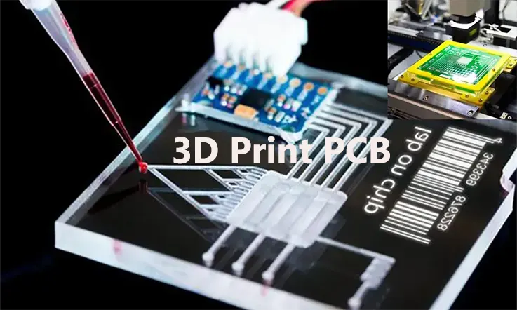
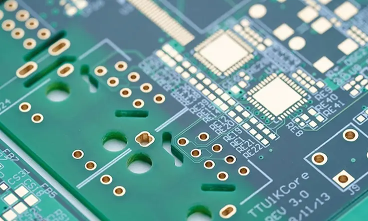
What is a 3D Print PCB?
When referring to a 3D PCB, it should be noted that it does not imply a three-dimensional circuit board. Rather, a 3D PCB is a type of circuit board manufactured using a 3D printer. In this process, the board’s circuits are printed directly onto the bare board using a 3D inkjet printer, eliminating the need for traditional copper etching techniques.
A 3D PCB employs a 3D inkjet printer equipped with an extruder head, which utilizes specialized gel or conductive materials. This printer is capable of accurately printing circuits onto a bare PCB board. The utilization of 3D printing technology in PCB manufacturing offers several advantages over conventional methods, including reduced errors and minimized waste material. The adoption of 3D PCBs has had a significant impact on the electronics manufacturing industry.
It is worth noting that 3D printing can produce both single-sided and double-sided PCBs with relative ease. Furthermore, applying a 3D printer to a flexible PCB is a straightforward process. However, printing a multilayer board presents a more complex challenge, which can be facilitated through the utilization of PCB design software.
Methods of 3D Printing PCBs
3D printing of printed circuit boards (PCBs) is a relatively new technology that allows for the quick prototyping and production of complex electronic devices. The major methods of 3D printing PCBs are as follows:
Fused Deposition Modelling (FDM)
FDM is the most common method of 3D printing. It works by heating and extruding a thermoplastic filament layer by layer onto a build plate. In the case of PCBs, a conductive filament can be used to create the circuit pathways.
Though FDM is not typically used for creating commercial-grade PCBs due to its relatively low resolution, it can be useful for prototyping simple circuits and for educational purposes.
Inkjet Printing
Inkjet printing involves depositing droplets of conductive ink onto a substrate. The ink is typically composed of silver or other conductive metals. The droplets of ink are deposited in the shape of the desired circuit pattern, and once the ink is dried or cured, a conductive pathway is formed.
Inkjet printing allows for the creation of complex, high-resolution circuits, making it suitable for commercial applications. However, the inks used can be expensive, and the process requires precise control over the deposition of the ink.
Aerosol Jet Printing
Aerosol jet printing is similar to inkjet printing, but instead of depositing droplets of ink, it sprays a fine mist of conductive ink onto the substrate. This allows for the creation of very fine, high-resolution circuit pathways.
Aerosol jet printing can be used to create complex, 3D circuits on a variety of substrates, making it a versatile method for 3D printing PCBs.
Selective Laser Sintering (SLS)
SLS involves using a high-power laser to fuse small particles of plastic, metal, ceramic, or glass powders into a mass that has the desired 3-dimensional shape. SLS can be used to create PCBs by using a conductive powder to form the circuit pathways.
SLS allows for the creation of complex, high-resolution circuits, and it can be used with a variety of materials. However, it requires a high-power laser and precise control over the sintering process.
Direct Laser Writing (DLW)
DLW is a method that uses a focused laser beam to pattern a photosensitive material. The laser beam alters the properties of the material, creating conductive pathways. This method can be used to create high-resolution, complex circuits.
DLW is a relatively slow process, but it allows for a high degree of control over the circuit design, making it suitable for creating complex, high-performance circuits.
It’s important to note that while 3D printed PCBs have many advantages, such as rapid prototyping and the ability to create complex circuits, they currently do not match the performance and reliability of traditional PCBs. However, as 3D printing technology continues to advance, the gap is likely to narrow.
Benefits and Challenges of PCB 3D Printing
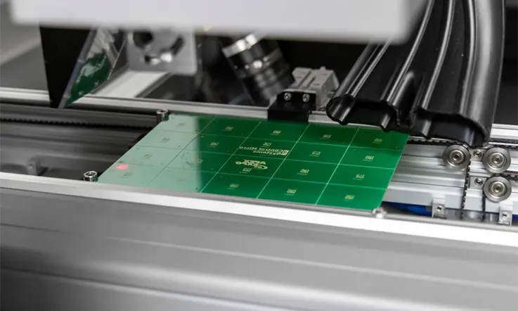
3D printing technology has significantly transformed many industries, and the electronics sector is no exception. Printed circuit board (PCB) 3D printing is one of the emerging technologies that has the potential to revolutionize the way we design and manufacture electronic devices. This technology involves the use of additive manufacturing to create a PCB layer by layer.
Let’s look at both the benefits and challenges of 3D-printed PCBs:
Benefits
Rapid Prototyping: One of the most significant advantages of PCB 3D printing is the ability to quickly create prototypes. Designers can print a circuit board, test it, modify the design, and reprint it in a short period, accelerating the development process.
Complex Designs: Traditional manufacturing methods can limit the complexity of the PCBs. 3D printing allows for more intricate designs, including multi-layer PCBs with integrated components.
Cost-Effective for Small Runs: Traditional PCB manufacturing involves high setup costs, making it expensive for small production runs. However, 3D printing can be cost-effective for producing small quantities.
Reduced Waste: 3D printing is an additive process, where material is added layer by layer, which can reduce waste compared to traditional subtractive manufacturing methods.
Customization: 3D printing allows for high levels of customization without significantly increasing costs. This can be beneficial for making customized electronics or devices for specific applications.
Challenges
Limited Materials: Currently, there are limitations on the types of materials that can be used for 3D printing PCBs. Typical 3D printers use thermoplastics, which may not have the necessary electrical properties for some applications.
Resolution and Precision: While 3D printing technology continues to improve, traditional manufacturing methods can often provide higher resolution and precision. This can be a significant challenge for PCBs, which often require precise, miniaturized components.
Speed: 3D printing is generally slower than traditional manufacturing methods, especially for large quantities. This makes it less suitable for mass production.
Durability and Quality: While 3D printed PCBs are suitable for prototyping, there may be concerns about their durability and quality for long-term use or in harsh environments.
Regulatory Challenges: As with any new technology, there can be regulatory challenges. Standards and regulations for 3D printed electronics are still in development, which could slow adoption.
In conclusion, while PCB 3D printing offers many advantages like rapid prototyping, complex designs, and cost-effectiveness for small runs, it also faces challenges such as limited materials, lower precision, slower speed, and concerns about durability and quality. Despite these challenges, as the technology continues to evolve, it is likely to become an increasingly important tool in electronics design and manufacturing.
Applications of 3D Printed Circuit Boards
3D printed circuit boards (PCBs) offer several unique advantages and applications compared to traditional PCB manufacturing methods. Here are some of the applications of 3D printed circuit boards:
Rapid Prototyping: 3D printed PCBs allow for rapid prototyping of electronic circuits. Design iterations can be quickly implemented and tested, reducing the time and cost involved in developing new electronic devices.
Custom Electronics: 3D printing enables the creation of custom-shaped PCBs that can fit into unconventional or compact spaces. This is particularly useful in devices with complex geometries or wearable electronics where space is limited.
Embedding Components: With 3D printed PCBs, components can be directly integrated into the printed structure, eliminating the need for additional assembly steps. This enables the creation of highly integrated devices with reduced size and weight.
Lightweight Electronics: By utilizing additive manufacturing techniques, 3D printed PCBs can be designed with lightweight structures, which is beneficial in applications such as drones, satellites, and aerospace systems, where weight reduction is critical.
Antenna Integration: 3D printed PCBs can incorporate antennas directly into the structure. This allows for the creation of compact and customized antennas that are well-suited for wireless communication devices.
Low-Volume Production: For low-volume production runs, 3D printing can be a cost-effective alternative to traditional PCB manufacturing methods. It eliminates the need for expensive tooling and setup, making it suitable for small-scale production or customized electronic devices.
Education and Research: 3D printed PCBs are valuable tools for educational institutions and research laboratories. They provide a hands-on learning experience for students, allowing them to design and fabricate functional circuits more easily.
IoT Devices: Internet of Things (IoT) devices often require compact and customized electronics. 3D printed PCBs can be used to create IoT devices with integrated sensors, microcontrollers, and wireless communication modules.
Flexible Electronics: Some 3D printing technologies allow for the creation of flexible PCBs. This flexibility is advantageous in applications where the circuit needs to conform to curved surfaces or undergo bending and stretching, such as wearable electronics or medical devices.
Repair and Replacement: 3D printed PCBs can be used to create replacement parts for legacy systems or obsolete components. This can extend the operational lifespan of older equipment that is no longer supported by traditional manufacturing methods.
It’s worth noting that while 3D printed PCBs offer several advantages, they also have limitations. The level of complexity and density achievable with 3D printed PCBs may be lower compared to traditional manufacturing methods. Additionally, the electrical and thermal properties of the printed materials may differ from those of conventional PCB materials, which can impact performance and reliability.
How to Choose the Optimal 3D Printing Process for PCBs?
Selecting the appropriate 3D printing process for your PCBs requires careful consideration of various factors. To make an informed decision, follow these steps:
1. Understand your requirements: Begin by clearly defining your project’s specific requirements. Consider factors such as the complexity of the circuit design, desired conductivity, mechanical strength, weight limitations, cost constraints, and any other relevant specifications.
2. Research available processes: Thoroughly investigate the 3D printing processes commonly used for PCB manufacturing, such as Fused Deposition Modeling (FDM), Multi Jet Fusion (MJF), or lamination methods. Understand the principles behind each process, their strengths, limitations, and the materials they are compatible with.
3. Evaluate material properties: Assess the conductivity, thermal and electrical properties, and mechanical strength of the materials compatible with each printing process. Compare these properties against your project requirements to ensure they align with the intended application of the PCB.
4. Consider design complexity: Determine the complexity of your circuit design. Some 3D printing processes may be better suited for intricate and densely packed designs, while others may struggle with fine details or multiple layers. Evaluate the capabilities of each process in relation to your design complexity.
5. Review cost considerations: Examine the cost implications associated with each 3D printing process. Evaluate not only the initial investment required for the printer but also the recurring expenses for materials, maintenance, and post-processing. Consider the long-term cost-effectiveness of each process for your specific production volumes.
6. Seek expert advice: Consult with experts or professionals experienced in 3D printing and PCB manufacturing. They can provide valuable insights and recommendations based on their knowledge and expertise, helping you make an informed decision.
7. Test and iterate: Before committing to mass production, consider prototyping and testing your PCB designs using different 3D printing processes. This hands-on experimentation will allow you to evaluate the quality, performance, and compatibility of each process with your specific requirements.
By carefully considering these steps and thoroughly researching the available options, you can confidently choose the most suitable 3D printing process for your PCB manufacturing needs. Remember to prioritize the alignment of material properties, design complexity, cost considerations, and expert advice to ensure successful outcomes.
What Are The Different Between PCB Manufacturing and 3D Printing PCB?
PCB manufacturing and 3D printing PCB are two distinct approaches to producing printed circuit boards, each with its own characteristics and processes. Here are the key differences between them:
Manufacturing Techniques
PCB Manufacturing: Traditional PCB manufacturing involves a subtractive process. It starts with a copper-clad substrate, and various steps such as etching, drilling, and plating are employed to create the desired circuit pattern.
3D Printing PCB: 3D printing, also known as additive manufacturing, builds PCBs layer by layer. It uses specialized 3D printers that deposit materials, such as conductive inks or resins, to create the circuitry and components in a three-dimensional manner.
Design Flexibility
PCB Manufacturing: Traditional manufacturing techniques offer a high level of design flexibility. Complex circuitry, multiple layers, and various components can be easily accommodated.
3D Printing PCB: 3D printing enables unique design possibilities, such as embedding components within the PCB, creating unconventional shapes, and integrating intricate geometries. This allows for greater design freedom but may have limitations in terms of electrical performance and material selection.
Prototyping and Customization
PCB Manufacturing: Traditional PCB manufacturing is well-suited for mass production but can be time-consuming and costly for prototyping or small-scale customization.
3D Printing PCB: 3D printing excels in rapid prototyping and low-volume customization. It enables quicker design iterations, reduces setup costs, and facilitates on-demand production of customized PCBs.
Material Selection
PCB Manufacturing: Traditional PCB manufacturing primarily uses rigid materials, such as FR-4, which offer good electrical performance and durability.
3D Printing PCB: 3D printing allows for a wider range of material options, including conductive inks, flexible substrates, and even composite materials. However, the electrical properties and mechanical strength of these materials may vary compared to those used in traditional PCBs.
Production Scale
PCB Manufacturing: Traditional PCB manufacturing processes are highly scalable, making them suitable for large-scale production.
3D Printing PCB: 3D printing is more commonly used for smaller-scale production, prototyping, and customized applications. Scaling up 3D printing for mass production can be challenging due to limitations in speed and material compatibility.
It’s important to note that both approaches have their strengths and are often used in conjunction with each other. PCB manufacturing is well-established and widely adopted, offering reliability and efficiency for large-scale production. 3D printing PCB, on the other hand, is favored for its design flexibility, rapid prototyping capabilities, and customization options.
Future of 3D Printed Circuit Boards
The future of 3D printed circuit boards (PCBs) holds immense potential for the electronics manufacturing industry. Here are some key aspects that shape the future of 3D printed PCBs:
Advancements in Materials: Ongoing research and development efforts are focused on expanding the range of materials suitable for 3D printing PCBs. This includes the development of conductive inks, flexible substrates, and multi-functional materials that offer enhanced electrical and mechanical properties. The availability of a wider selection of materials will enable the production of more diverse and complex PCB designs.
Improved Printing Technologies: 3D printing technologies continue to evolve, becoming more precise, efficient, and capable of producing intricate PCB structures. Advancements in printing techniques, such as higher resolution and finer nozzle sizes, will enable the creation of smaller components and finer circuit traces. Enhanced printing technologies will facilitate the production of complex multilayer boards with improved reliability and performance.
Integration of Electronics and Structures: 3D printing allows for the seamless integration of electronic components within the physical structure of a product. This opens up new possibilities for embedding sensors, antennas, and other circuitry directly into objects, enabling the creation of smart and connected devices. This integration of electronics and structures can lead to innovative applications in fields like healthcare, automotive, aerospace, and IoT.
Design Freedom and Customization: 3D printing offers unparalleled design freedom, enabling the creation of highly customized PCBs tailored to specific applications. Designers can optimize the circuit layout, shape, and orientation to maximize performance and functionality. This customization potential allows for rapid prototyping, iterative design improvements, and the production of small-batch or on-demand PCBs, reducing time-to-market and overall costs.
Sustainability and Waste Reduction: 3D printing can contribute to sustainable manufacturing practices by minimizing material waste compared to traditional subtractive manufacturing methods. With precise material deposition, only the required amount of material is used, reducing scrap. Additionally, advancements in recyclable and eco-friendly materials for 3D printing contribute to a more sustainable PCB manufacturing process.
Integration with AI and Automation: The integration of 3D printing with artificial intelligence (AI) and automation technologies holds promise for streamlining the PCB manufacturing process. AI algorithms can optimize designs for additive manufacturing, enhance quality control, and automate post-processing tasks. This integration will lead to increased efficiency, productivity, and scalability in 3D printed PCB production.
Overall, the future of 3D printed PCBs is poised for significant advancements in materials, printing technologies, design capabilities, sustainability, and automation. These developments will revolutionize the electronics manufacturing landscape, enabling the production of highly customized, efficient, and integrated PCBs for a wide range of applications.
Summary
The advent of 3D printed circuit boards is revolutionizing the landscape of electronics design and production. By harnessing the capabilities of 3D printing technology, developers now have the ability to fabricate circuit boards in virtually any desired shape. This newfound flexibility fosters a heightened level of creativity and innovation within the electronics industry.
To explore further details about the potential of 3D printed circuit boards, we invite you to get in touch with Circuits Central. Our knowledgeable team is available to provide comprehensive information and address any inquiries you may have. Please feel free to reach out to us at 0086-0755-23034656 or by contacting us through our website. We look forward to assisting you in unlocking the possibilities offered by 3D printed circuit boards.
Related Posts:
1. What Is PCB Etching and How to Make a perfect PCB Etching?
2. The Best PCB Panelization Guide
4. Understanding PCB Delamination: A Comprehensive Guide
5. The Best Backplane Printed Circuit Boards Factory
6. An Overview of Through-hole Technology (THT)
7. Detail Talk Surface Mount Technology