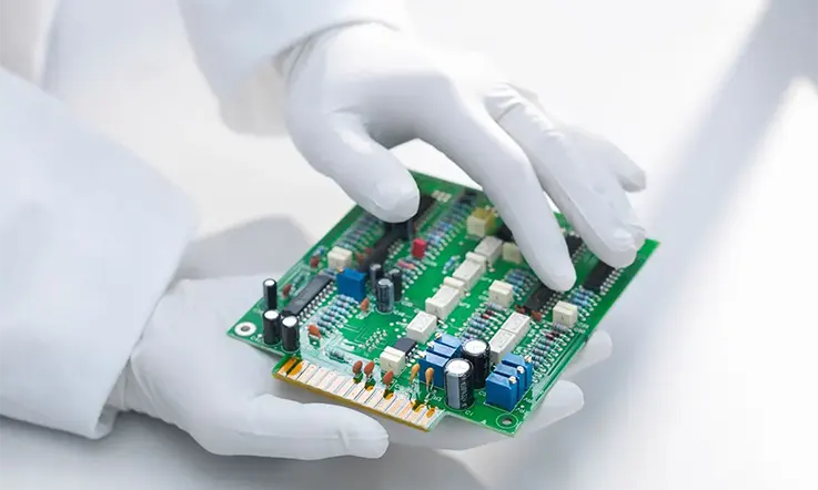
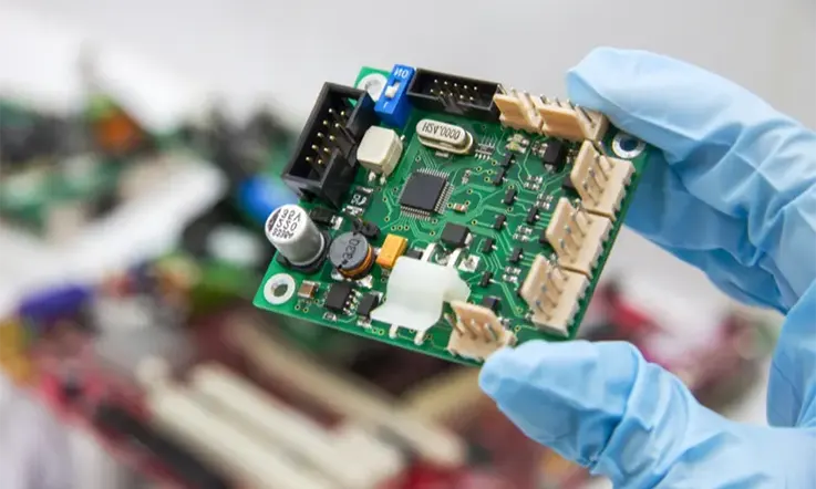
Printed circuit boards (PCBs) are an essential part of many electronic devices, from smartphones and laptops to medical equipment and automotive systems. PCBs can be complex and expensive to design, so some companies or individuals may opt to try to clone an existing PCB instead of designing a new one from scratch. PCB cloning involves analyzing and reproducing an existing circuit board, so it looks and works the same as the original. Cloning can be a cost-effective way to produce additional copies of a PCB design, but it is important to be aware of the potential legal and ethical issues surrounding PCB cloning.
In this article, we will explore the process of PCB cloning and discuss some of the considerations that should be taken into account before embarking on a PCB cloning project.
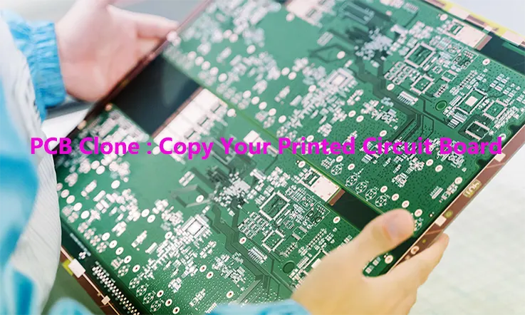
What Is PCB Clone ?
PCB clone, also referred to as PCB duplication or PCB duplicate, involves using reverse engineering technology to create an exact copy of an existing printed circuit board. The process typically entails two steps – creating the Bill of Materials (BOM) and duplicating the schematic diagrams of the original circuit board, as well as understanding the design parameters and manufacturing protocols. You are not required to provide PCB Gerber files, as electronic specialists will analyze the files to deduce the PCB’s design and generate a replica board.
By using PCB cloning, the original PCB board can be replicated and installed in an electronic device, thereby eliminating the need to design and fabricate new circuit boards from scratch. This means that you can copy the entirety or a percentage of the printed circuit boards without affecting their performance, thus providing you with enhanced flexibility and the ability to produce infinite boards as per your preferences.
Moreover, electronic manufacturers can utilize the PCB clone method to streamline labor, cutting down on the amount of time and money spent in redesigning circuit boards. Furthermore, it allows replacement of electronic components that are no longer operating efficiently. Reverse engineering is a vast improvement compared to traditional manufacturing methods, thereby making the PCB clone process highly beneficial for the contemporary electronic industry. At JarnisTech, we are dedicated to providing superior PCB cloning services that align with the highest industry standards to ensure.
Types of PCB Clone
There are two main types of PCB clone:
● Hard Copy Cloning: Also known as physical or traditional cloning, this method involves physically reproducing the original PCB by scanning, tracing, or manually copying the layout and connections onto a new board.
● Digital Cloning: Also known as reverse engineering, this method involves creating a digitized copy of the original PCB by scanning it with a 3D scanner or converting the PCB layout files into a digital format that can be used to reproduce the board.
The PCB cloning service is a streamlined process that aids in the creation of a precise electronic circuit board layout without the need for a time-consuming board design process. PCB cloning also has the potential to result in significant cost savings for individuals and businesses.
At JarnisTech, we understand the importance of providing high-quality PCB cloning services that meet our clients’ unique requirements. Our team of experienced professionals and use of advanced technology ensures that the PCB cloning process is efficient and cost-effective, delivering top-grade PCBs that align with the industry’s highest standards.
How Many Steps Clone PCB Boards ?
The process of cloning a PCB is a streamlined and automated operation that requires specific tools and components.
Before commencing the PCB cloning process, it’s crucial to have a Bill of Materials (BOM) and a copy of the circuit schematics. Additionally, you need to select a research method that suits your specific requirements from a wide range of options.
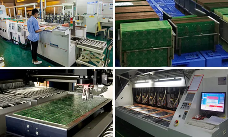
In terms of tools, it’s necessary to have an AutoCAD program, a computer, a scanner, and a PROTEL99 to streamline the process of PCB cloning. These essential tools ensure that the method of reverse engineering is carried out efficiently and effectively, delivering precise PCB replicas that function seamlessly.
PCB Clone Steps
The process of cloning a PCB involves a series of specific steps that require attention to detail and accuracy to achieve optimal results.
When cloning, the actions listed below should be followed in order:
● Initially, you must remove all active components from the PAD hole and the tin, followed by cleaning the board using an ultrasonic cleaner. Afterward, place the empty board on the scanner and scan it horizontally, ensuring that the brightness and contrast settings are correct for viable image quality.
● The next step is to import the scan into Photoshop, where both bottom and top screen-printing techniques are comparable. Buff the surface of both top and bottom layers of the board using paper yarn and then use Photoshop to perform a color sweep across both layers.
● At this point, it’s necessary to adjust the brightness, lightness, and contrast of the image to check for clear image lines. If the image is unclear, either restart the process or utilize Photoshop to adjust the sketch. If the image is clear, save it as a black and white BMP file.
● The BMP files must then be converted into a PROTEL file using PROTEL99, followed by generating two levels using the PROTEL file. Open both imported CAD files and using the image of the PCB as a reference, transfer the component package into the CAD program, position the pads and vias in the appropriate locations and measure the pads’ outer and inner dimensions.
● Next, draw a line on the TOP Layer to install the device, erase the silk layer, convert the PCB to PROTEL, combine the two diagrams into one, and print both layers onto transparent film in a 1:1 ratio. Position the film over the board and check for any errors.
● Finally, test the cloned PCB to ensure it functions like the original. Please note that cloning a PCB requires expert attention to detail and accuracy, and alternatively can be carried out by a professional PCB clone service provider. At JarnisTech, we offer top-quality PCB cloning services that guarantee superior results and customer satisfaction.
Precautions When Cloning a PCB
Here are some precautions to take when cloning a PCB:
● Obtain the latest version of the PCB layout files and make sure there are no errors or inconsistencies before beginning the cloning process.
● Use high-quality materials and components to ensure the cloned PCB performs as well as the original.
● Take accurate measurements of the original PCB and use a digital caliper to ensure the cloned PCB matches the dimensions precisely.
● Use a high-quality scanner or camera to obtain an accurate image of the original PCB layout.
● Make sure you have the appropriate software and skills necessary to recreate the original PCB. PCB layout software such as Eagle PCB, Altium Designer and KiCad are all good options.
● Double-check the connection and component placement before finalizing the design.
● Verify the cloned PCB works as intended by testing it with the original device and observing its performance.
● Take care when soldering to ensure all components are correctly mounted and there are no short circuits.
● Always wear appropriate personal protective equipment when handling PCB materials and chemicals, such as gloves, eye protection, and a respirator if necessary.
● Dispose of any waste materials safely and responsibly.
Examples of PCB Cloning in Various Applications
Here are some examples of PCB cloning in various applications:
● Electronics repair: PCB cloning is commonly used in electronics repair, where a faulty circuit board can be replicated, tested, and replaced without having to develop a new design.
● Automotive industry: PCB cloning is used in the automotive industry to replicate legacy systems, such as engine control units (ECUs) or body control modules (BCMs), for repairing or replacing aging vehicles.
● Aerospace industry: PCB cloning is used in the aerospace industry to replicate circuit boards used in flight control systems or communication systems. This ensures consistency in the performance of the systems across different missions.
● Medical devices: PCB cloning is used in the medical device industry to replicate circuit boards for repairing or replacing aging or obsolete equipment, such as patient monitors, infusion pumps, or diagnostic instruments.
● Military and defense: PCB cloning is used in military and defense applications to replicate circuit boards for repairing or upgrading legacy systems, such as communication devices or missile guidance systems.
● Consumer electronics: PCB cloning is used in the consumer electronics industry to replicate circuit boards for repairing or upgrading various devices, such as smartphones, laptops, and gaming consoles.
In each of these examples, PCB cloning allows for the replication of existing circuit board designs, saving time and reducing costs, while ensuring consistency and performance in critical applications.
Advantages of PCB Clone
The field of engineering stands to gain several benefits from the utilization of reverse engineering methods, such as examining present designs, recreating outdated products, and producing cost-effective alternatives. PCB cloning services from Jarnis Technology can provide a range of benefits and advantages, including:
● Customization: Our PCB cloning service enables customers to fully customize their electronic circuit board to meet their specific requirements.
● Reduced time and cost: We employ advanced technology and reverse engineering methodologies to deliver PCB cloning services that are efficient and cost-effective.
● Improved efficiency: Our PCB cloning services help improve your electronic devices’ performance by enabling the replacement of obsolete PCBs with modern, cloned PCBs that function optimally.
● Enhanced flexibility: With the provision of multiple cloned PCBs, customers can develop a range of products that require electronic circuit boards.
● Access to expert knowledge: Jarnis Technology has a team of qualified engineers and professionals that can provide expert guidance and support throughout the PCB cloning process.
Disadvantages of PCB Clone
Here are some possible disadvantages of PCB clone:
● Limited flexibility: PCB clone recreates an exact copy of an existing PCB, which means that you have limited flexibility to modify the design or circuits. You may be limited to the components used in the original board, which may not be the most efficient or cost-effective solution for your needs.
● Intellectual property concerns: PCB clone may raise intellectual property (IP) concerns, particularly if the original PCB is protected by patents or copyrights. Reproducing a PCB design without permission may lead to legal issues and affect your reputation.
● Quality issues: PCB cloning may result in quality issues if the original PCB is damaged or has errors. It may be difficult to identify and correct these issues, leading to performance problems or malfunctions.
● Compatibility issues: PCB clone may have compatibility issues with newer components or technologies, which may not have been available or widely used when the original PCB was designed.
● Time-consuming: PCB clone may still take a significant amount of time to complete, particularly if you need to reverse engineer the original PCB design or identify and resolve issues with the reproduction.
● Cost: PCB clone may be cheaper than creating a new PCB from scratch, but it may still be more expensive than other repair or replacement options, particularly if the original PCB is obsolete or hard to find.
How Does PCB Cloning Help in PCB Development and Redesign ?
Printed circuit board (PCB) cloning is a contemporary information technology application that employs reverse engineering methodologies to build PCB design boards. While creating a new PCB product from scratch typically requires a significant amount of time, PCB redesigning has become a more straightforward process thanks to advancements in printed circuit board cloning techniques and reverse engineering approaches.
Given the rapid pace of technological advancement, electronic components must be upgraded frequently, yet conventional PCB design methods often struggle to accommodate such ongoing improvements. Hence, the adoption of PCB reverse engineering is rapidly increasing in new high-tech systems.
As a result, modern PCB design engineering is embracing reverse engineering techniques such as cloning to enable the reproduction and upgrading of existing PCBs effectively. This way, PCB redesigning can be achieved efficiently, enabling electronic component upgrades to occur promptly.
How to Operate for Your PCB Cloning Project ?
● To initiate your PCB cloning project, please send sample photos to [email protected] where our proficient engineers will offer a preliminary estimate of the cost. If you have the project specifications, kindly inform us, or alternatively, provide clear photographs of the integrated circuits.
● Once you submit your sample (two samples if possible), our team will evaluate and offer an accurate price quote. It’s worth noting that some ICs need a program crack, which we will separate and quote accordingly.
● From here, we commence the PCB cloning process, and upon completion, which includes a thorough quality control check, we will email you the Gerber files, the schematic diagram, and the Bom List (if applicable). At JarnisTech, we aim to offer seamless PCB cloning services that meet and exceed customer expectations.
Now that the PCB cloning process has been completed, we will swiftly begin the process of producing the circuit board as per your requirements.
Printed circuit boards (PCBs) are an integral component of modern electronic devices, and their demand has risen due to advancements in electronic gadget manufacturing. As a result, manufacturers are currently producing a fresh batch of PCBs to meet the ever-increasing needs of electronic designers.
Cloning PCBs holds immense significance for various reasons, one of which is replacing obsolete PCBs for which there are no longer supplies available. In the industry, one of the significant challenges is replacing outdated PCBs with modern ones in high-frequency applications. Therefore, it is crucial to understand the PCB cloning process, its benefits, and how it operates to comprehend the significance of the PCB clone service.
At JarnisTech, we strive to provide an efficient and dependable PCB cloning service that meets our clients’ specific needs. We employ state-of-the-art technology and the latest procedures to ensure that our cloned PCBs function exceptionally well, and deliver timely customized solutions to our customers.
What Techniques Are used to PCB Clone ?
Here are some common techniques used in PCB cloning:
● Visual inspection: This involves closely examining the physical characteristics of the original circuit board, including the layout, component placement, and trace routing, to obtain a visual representation of the board.
● Schematic tracing: This involves tracing the electrical connections on the original circuit board to create a schematic diagram of the circuit design.
● Reverse engineering: This involves creating a detailed CAD file of the circuit board from a physical board, either manually or through software-aided techniques.
● Circuit testing: This involves verifying the functionality of the original circuit board through various tests, such as functional testing, boundary scan testing, or flying probe testing.
● Component identification: This involves identifying the specific components used in the original circuit board and obtaining equivalent or compatible components for use in the cloned board.
● Soldering and assembly: This involves soldering the components onto the cloned PCB and assembling it into a functional electronic system.
In general, a combination of these techniques is used to recreate a functional replica of the original circuit board design with a high degree of accuracy and reliability. The specific techniques used may vary depending on the complexity of the circuit and the required level of precision needed for the cloned board.
Comparison of PCB Clone with Other Similar Techniques
Here’s a brief comparison of PCB clone with other similar techniques:
● PCB Replication: PCB replication involves creating a new board that is functionally equivalent to the original board. Like PCB clone, replication replicates the layout and interconnections of the original board, but it doesn’t attempt to create a copy that is identical in all aspects. Replication is generally faster and less expensive than clone, but may require more processing power due to slight variations in the layout.
● PCB Design Modification: PCB Design Modification involves making changes to an existing PCB layout to add new features, improve functionality or optimize form factor. While PCB clone attempts to reproduce a board exactly, PCB Design Modification can be used to improve the design in various ways.
● PCB Layout Reuse: PCB layout reuse refers to the process of taking an existing PCB layout and reusing it for a new design. This can save time and money compared to creating a new layout from scratch, but it assumes that the existing layout meets the needs of the new design. Unlike PCB clone, layout reuse doesn’t require creating a duplicate of the original board.
As a result, PCB clone is best suited for cases where an identical or modified copy of the original PCB is required for repair or replacement purposes. Other methods such as PCB replication, design modification, and layout reuse are better for cases where only certain aspects of the original PCB need to be replicated or modified.
Differences between PCB Clone and PCB Design
Here are some possible differences between PCB clone and PCB design:
● PCB clone is the process of duplicating or reproducing an existing printed circuit board (PCB) while PCB design involves creating a new PCB layout from scratch.
● PCB clone uses an existing PCB as a reference or blueprint, while PCB design starts with a product specification and requires designing all PCB details from scratch.
● PCB clone aims to recreate an exact copy of an existing PCB, while PCB design has more flexibility to modify the circuit and layout to fit specific requirements.
● PCB clone may be used for various reasons such as replacing broken parts or updating outdated designs, while PCB design is typically used for creating new and innovative products.
● PCB clone requires the physical possession of an existing PCB for reference, while PCB design can be done remotely with the help of computer-aided design (CAD) software.
● PCB clone may have limitations in terms of component availability and compatibility, while PCB design can choose and integrate any available electronic components.
● PCB clone may be considered a quicker and more cost-effective solution for reproducing an existing PCB, while PCB design may take longer and involve more planning and testing.
When to Use PCB clone or PCB Design ?
Here are some scenarios where you might choose to use PCB clone or PCB design:
When to Use PCB Clone:
● You need to reproduce an existing PCB that is no longer available or repair a faulty PCB.
● You want to update an existing PCB design without altering its original functionality or performance.
● You need to create multiple copies of the same circuit board.
● You want to reverse engineer a product that uses a proprietary or obsolete PCB design.
When to Use PCB Design:
● You need to design a custom PCB for a new product or feature.
● You want to optimize an existing PCB design for better performance or cost-effectiveness.
● You need to incorporate new components or technologies that are not currently available on the market.
● You want to create a highly unique and customized PCB that is tailored to your specific needs.
In general, PCB clone may be a good choice when you need to reproduce an existing PCB quickly and cost-effectively, while PCB design is more suitable for creating new and innovative products or customizing existing designs to meet specific requirements.
Future Implications for PCB Cloning
The future implications for PCB cloning may include:
● Increased efficiency: PCB cloning may continue to improve, becoming faster and more efficient, enabling companies to improve their production processes and reduce the time and costs of creating new PCB designs.
● Accessibility: As PCB cloning techniques become more widespread and accessible, smaller companies and hobbyists may be able to create their own PCB clones, increasing innovation and competition in the industry.
● Intellectual property concerns: As PCB cloning becomes more prevalent, new legal and ethical concerns may arise around intellectual property and the protection of original designs.
● New applications: The ability to clone existing PCBs may enable new applications and technologies that were previously not possible, leading to further advancements in electronics and other related fields.
Integration with AI: PCB cloning techniques may become more integrated with artificial intelligence and machine learning algorithms, enabling automation and optimization of the PCB design process.
Conclusion
The electronic industry is currently undergoing rapid development characterized by innovative product and process developments. PCB cloning is an important aspect of the electronic manufacturing process, particularly when electronic component manufacturers wish to update the designs of their printed circuit boards (PCBs) in response to new innovations in the market.
At JarnisTech, we offer top-of-the-line PCB clone and bulk manufacturing services for customers seeking high-end PCB and PCBA clone solutions. Our team of highly competent and well-trained professionals possesses years of experience in the PCB industry, delivering superior results to our customers and a flawless track record of excellence.
We believe that this post has provided valuable insight into the importance of PCB cloning, and we remain available to address any additional inquiries you may have concerning our PCB cloning services. Choose JarnisTech for unparalleled PCB manufacturing solutions and a customer-centric approach that ensures exceptional outcomes and customer satisfaction.
Related Posts:
1. What Is PCB Etching and How to Make a perfect PCB Etching?
2. The Best PCB Panelization Guide
3. The Importance of 3D Printed PCBs in Modern Electronics Production
4. Understanding PCB Delamination: A Comprehensive Guide
5. The Best Backplane Printed Circuit Boards Factory
6. An Overview of Through-hole Technology (THT)