The field of modern energy storage merges two distinct disciplines: electrochemistry and electronics. The chemical composition of a battery cell defines its energy potential; the electronics governing it dictate its realized performance, safety profile, and operational lifespan. This text provides a detailed analysis of contemporary battery technologies, with a specific focus on the sophisticated Printed Circuit Board (PCB) assemblies that form the foundation of any advanced Battery Management System (BMS). It explores the design intricacies, material science, and fabrication considerations that enable the next generation of power solutions.
The Function of the Battery Management System (BMS)
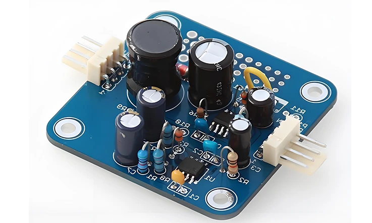
A Battery Management System (BMS) governs the operation and performance of a battery pack. As an electronic system built upon a Printed Circuit Board (PCB), it oversees all operational aspects. A malfunction within the BMS, often stemming from the circuit board itself, can lead to the failure of the entire pack.
State of Charge (SOC) and State of Health (SOH) Estimation
The BMS calculates the battery’s available energy (State of Charge) and assesses its long-term degradation (State of Health). These determinations are derived from high-precision measurements of cell voltage, current, and temperature. The precision of these estimations is a direct consequence of the signal integrity maintained by the PCB. A well-executed board layout and fabrication process minimizes signal distortion, providing the microcontroller with accurate data.
Cell Balancing
Manufacturing variations mean that individual cells in a pack have slight differences in capacity and internal resistance. The BMS uses balancing circuits, physically located on the PCB, to equalize the charge level across all cells. This process maximizes the pack’s usable capacity and can extend its operational lifespan by 10-20%. The effectiveness of these balancing circuits is dependent on the PCB’s thermal design and component assembly.
Safety and Protection
The BMS provides a layer of protection against hazardous conditions. Its circuitry, housed on the PCB, is designed to disconnect the battery from the load or charger to prevent:
●Over-voltage and under-voltage events
●Over-current situations
●Temperatures outside of the designated operating range
The dependability of these protective measures is directly related to the manufacturing and assembly quality of the Printed Circuit Board.
Anatomy of a High-Performance BMS PCB
The Printed Circuit Board for a Battery Management System is a complex component, engineered to handle conflicting technical demands. It must route high-power currents while protecting sensitive, low-voltage measurement circuits, all within a compact footprint. Multi-layer constructions are the standard approach to resolving these challenges.
The board’s architecture addresses two main areas:
High-Power Circuit Management
BMS boards must manage substantial electrical loads, sometimes hundreds of amperes, which requires specific manufacturing and assembly solutions.
●Heavy Copper Traces: The manufacturing process utilizes heavy copper layers (e.g., 3oz, 4oz, or thicker) to reduce resistive heating and improve thermal dissipation.
●Embedded Busbars: For extreme current requirements, the assembly may involve embedding or soldering solid copper busbars directly onto the board, a specialized integration technique.
●Voltage Isolation: With system voltages reaching 400V or 800V, the fabrication process must ensure exacting clearance (air gaps) and creepage (surface distance) between conductors to prevent high-voltage arcing.
| Parameter | Typical Value | Purpose/Impact |
| Copper Thickness | 3oz – 6oz | Lower resistance, improved heat dissipation |
| Max Continuous Current | 100A – 300A | Ensures reliable operation without overheating |
| Busbar Cross-Section | 10mm² – 25mm² | Handles peak current surges without significant voltage drop |
| Clearance (Air Gap) | ≥ 6.4 mm @ 800V | Prevents arcing between high-voltage conductors |
| Creepage (Surface Distance) | ≥ 8 mm @ 800V | Prevents surface leakage currents in high-voltage applications |
Precision Signal Path Design
The board must provide a clean environment for measuring millivolt-level signals from each battery cell, which are susceptible to electromagnetic interference (EMI).
●Signal Isolation: A multi-layer architecture allows for routing these sensitive analog traces on dedicated internal layers, physically separated from noisy, high-current paths.
●Ground Planes: The inclusion of internal ground planes creates a stable reference and a short return path for signals, shielding them from interference and preserving the accuracy of measurements.
●Controlled Impedance: This structured layering, achieved through a precise fabrication process, establishes a controlled impedance environment necessary for dependable data acquisition.
| Parameter | Typical Value | Purpose/Impact |
| Signal Trace Width | 4 – 6 mil | Reduces noise pickup while maintaining controlled impedance |
| Differential Pair Spacing | 6 – 8 mil | Ensures balanced impedance and reduces crosstalk |
| Ground Plane Thickness | 1oz – 2oz | Provides low-impedance return path and EMI shielding |
| Analog-Digital Separation | ≥ 20 mm | Minimizes interference from switching circuits |
| Controlled Impedance Tolerance | ±10% | Ensures reliable, repeatable high-speed or precision analog signal measurements |
PCB Layout and its Influence on Firmware
In a BMS, the hardware and firmware are inseparable. The physical layout of the Printed Circuit Board has a direct effect on firmware operation and the efficiency of the development process. A layout that fails to account for this relationship can create significant downstream difficulties.
Key areas where the PCB layout affects firmware include:
Signal Timing and Communication
For peripherals like the Serial Peripheral Interface (SPI) that interface with an Analog Front-End (AFE), the physical length and routing of PCB traces determine signal propagation delay.
●Synchronization Issues: Mismatched trace lengths can cause data and clock signals to become misaligned, resulting in communication errors.
●Firmware Complications: These hardware-level timing issues force the firmware to compensate, often with slower clock speeds or more complex error-handling routines, reducing overall performance.
●Manufacturing Precision: Executing a layout with precisely matched trace lengths is a feature of a disciplined fabrication process that holds tight tolerances.
Accessibility for Programming and Debugging
The firmware development lifecycle depends on physical access to the microcontroller for programming and real-time diagnostics.
●Connector Placement: A thoughtful layout provides clear access to programming headers (e.g., JTAG, SWD), positioning them away from large components or mechanical housings.
●Assembly Considerations: Obstructions due to poor component placement during assembly can make connecting a debugger difficult, impeding development, testing, and field service.
Hardware Resource and Pin Assignment
The PCB routing must align with the microcontroller’s internal architecture to enable intended performance.
●Function-Specific Pins: For example, pins for high-frequency Pulse-Width Modulation (PWM) are often linked to dedicated hardware timers within the silicon.
●Enabling Hardware Acceleration: The board layout must route these signals to the correct physical pins. This allows the firmware to utilize the device’s hardware accelerators for timing-sensitive tasks, rather than resorting to less precise software-based emulation.
Therefore, the PCB is more than a substrate for components; it is an active part of the system’s computing architecture. Its design and fabrication have direct consequences on software behavior and reliability.
Battery Technology Leaders and Their PCB Demands
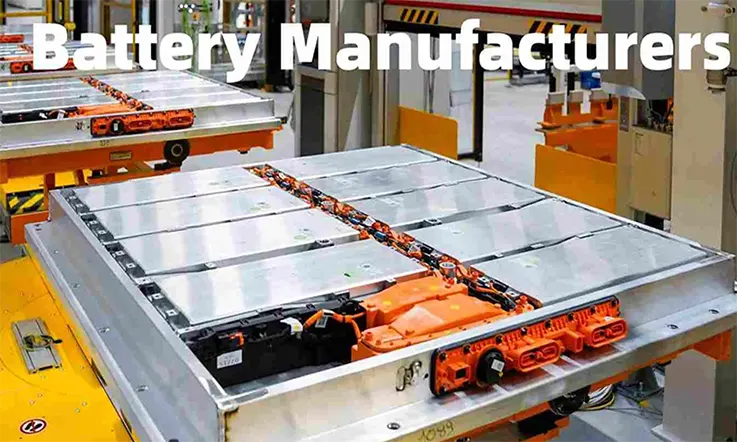
The following corporations are at the forefront of battery cell and system development. Their advancements in chemistry and mechanical architecture generate new demands for sophisticated electronic controls and the underlying PCB technology.
CATL (Contemporary Amperex Technology Co., Limited)
As a massive producer of electric vehicle batteries, CATL’s innovations in pack architecture directly influence the complexity of the BMS and its circuit board.
●Cell-to-Pack (CTP) Technology: This approach integrates cells directly into the pack, removing the intermediate module structure. It requires large-format or interconnected PCBs to manage signals and power across the pack’s entire area.
●Qilin Battery: This next-generation CTP design incorporates large-surface liquid cooling plates. The BMS circuit board for this system must be designed for tight mechanical and thermal integration with the cooling hardware.
BYD Company Ltd.
BYD’s vertical integration has enabled it to pioneer unique battery structures that merge energy storage with mechanical functions.
●Blade Battery: This design uses long, thin cells as structural members of the pack. The associated PCBs must also be long and narrow, capable of mounting sensors along their length to capture precise thermal and voltage data without signal degradation.
LG Energy Solution Ltd.
LG Energy Solution is a major supplier of high-energy pouch cells, particularly those with high-nickel NCM and NCMA chemistries.
●Pouch Cell Form Factor: The flexibility of pouch cells allows packs to fit non-rectangular spaces. This application often requires rigid-flex PCBs or multiple interconnected rigid boards, demanding advanced fabrication and assembly methods.
●High-Nickel Chemistry Management: These chemistries require exceptionally precise thermal and voltage control. The corresponding PCBs need to support high-sensitivity analog circuitry and fast-switching protection components, often necessitating specific material choices to manage performance.
Panasonic Corporation
Panasonic is a powerhouse in cylindrical cell production, known for mass-producing cells with remarkable uniformity for partners like Tesla.
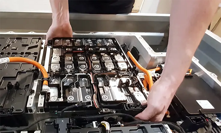
●Cylindrical Cell Architectures (e.g., 2170, 4680): Packs built from thousands of cylindrical cells typically use a hierarchical BMS. This creates a demand for two classes of boards: compact, cost-effective slave boards produced in high volume, and a sophisticated master controller with high processing power.
●4680 Cell Format: The larger 4680 cell’s tabless design alters the pack’s thermal profile. The BMS and the sensor placement on its PCBs must be adapted to accurately monitor these new thermal dynamics.
Samsung SDI Co., Ltd.
Samsung SDI is a leading producer of prismatic cells for the EV market and is also active in small-format batteries.
●Prismatic Cells: These rectangular cells offer high packaging efficiency. Their application in EVs leads to demand for modular PCB designs that can be reliably manufactured and assembled for various scalable pack configurations.
●High-Density Applications: For compact devices, the protection circuits require high-density interconnect (HDI) PCBs, featuring microvias and fine-line manufacturing processes.
Tesla, Inc.
Tesla’s brand is built on its battery and software technology, with its in-house BMS development being a core competency.
●Advanced BMS Algorithms: Tesla’s BMS is known for its accurate predictive models. The underlying PCBs must provide an exceptionally stable, low-noise platform to support the high-speed processors running this software.
●In-House ASIC Development: Tesla develops its own Application-Specific Integrated Circuits (ASICs). This requires a PCB manufacturing partner capable of handling designs with high-density layouts that are tightly coupled with proprietary silicon.
Bridging Design and Fabrication: DFM and DFA Principles
A theoretically sound design is only practical if it can be manufactured and assembled reliably at a reasonable cost. Design for Manufacturability (DFM) and Design for Assembly (DFA) are methodologies that align a design with real-world production capabilities. Engaging with these principles early prevents costly revisions and production delays.
Key considerations in this process include:
Panelization Strategy
Individual PCBs are produced on larger master panels. An optimal panelization scheme, often developed in consultation with the fabricator, maximizes the number of boards per panel to reduce material waste and lower per-unit cost. The strategy also incorporates features for automated assembly, such as V-grooves for clean separation and fiducial marks for machine vision alignment.
Component Selection and Footprint Design
A review against DFA principles helps guide the selection of components suitable for high-speed automated assembly.
●Standard Packages: Choosing standard component packages can improve placement speed and component availability.
●IPC-Compliant Footprints: The design of the copper pads (footprints) on the PCB is a direct factor in solder joint quality. Adherence to IPC standards for footprint dimensions ensures proper solder fillet formation and prevents common assembly defects.
Test Point Strategy
A product’s reliability is verified through testing, which requires access to the circuitry. A DFM analysis identifies optimal locations for dedicated test pads on the PCB. Planning these access points from the beginning enables efficient In-Circuit Testing (ICT) and Functional Circuit Testing (FCT) after assembly, reducing the cost of quality control.
Clearances and Tolerances
Every fabrication process has inherent physical limitations. DFM analysis verifies that clearances are appropriate for the design’s voltage requirements while remaining within the fabricator’s standard process capabilities. Requesting tolerances tighter than necessary can substantially increase costs and lead times without providing additional performance benefits.
Architecting for Agility: Modular and Scalable BMS Platform Design
For organizations developing a portfolio of products, a one-off design approach is inefficient. Adopting a modular and scalable platform architecture for the BMS allows for faster development cycles, reduced development costs, and greater product line flexibility. A manufacturing partner with versatile capabilities is a prerequisite for implementing such a strategy.
Key architectural patterns include:
The Configurable Platform
This methodology involves designing a core BMS PCB that can be adapted for a family of applications. For example, a single board layout might support battery packs from 10S to 16S configurations by populating or depopulating specific Analog Front-End (AFE) chips and their associated components. This approach relies on an assembly partner with robust process control to manage multiple Bill of Materials (BOM) variants on a single layout.
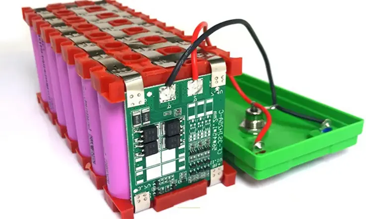
Master-Slave Architecture
For very large systems, such as grid-scale energy storage, a distributed master-slave architecture is employed. This approach requires a supplier capable of producing two distinct types of circuit boards efficiently.
●Slave Units (CMUs): Numerous small, cost-optimized Cell Monitoring Unit (CMU) boards are distributed throughout the pack. Their fabrication process must be tailored for high-volume production without sacrificing measurement precision or reliability.
●Master Controller: A single, more powerful master controller aggregates data from all slave units. The PCB for this master unit is typically a complex, low-volume board with high component density, demanding advanced fabrication and assembly capabilities.
Firmware Modularity
A modular hardware platform is paired with a corresponding modular firmware architecture. The software is structured with a Hardware Abstraction Layer (HAL) that allows the core application code to function across different hardware configurations. The success of this software strategy is predicated on the hardware being assembled with perfect fidelity to the design, ensuring the HAL interacts with a predictable and dependable physical layer.
Strategic Substrate Selection for BMS PCB Reliability
The choice of a PCB’s base material is an engineering decision that governs its thermal, electrical, and mechanical performance. This selection has a direct bearing on the final product’s reliability and cost. Different BMS applications demand different substrate properties.
FR-4: The Industry Standard
Flame Retardant 4 is a glass-reinforced epoxy laminate. It is the most common PCB substrate, offering a well-balanced profile of mechanical strength, electrical insulation, and cost-effectiveness for a wide range of applications.
| Parameter | Typical Value |
| Dielectric Constant (Dk) | 4.2 – 4.8 |
| Glass Transition Temp (Tg) | 130°C – 140°C |
| Thermal Conductivity | 0.3 – 0.4 W/m·K |
| Volume Resistivity | 10¹⁰ – 10¹² Ω·cm |
| Cost Level | Low |
High-Tg FR-4 for Elevated Temperatures
In applications with higher ambient or operating temperatures, such as in enclosed battery packs, High-Tg FR-4 is specified. With a glass transition temperature (Tg) of 170-180°C, this material maintains its structural integrity and performance where standard FR-4 would degrade.
| Parameter | Typical Value |
| Dielectric Constant (Dk) | 4.2 – 4.5 |
| Glass Transition Temp (Tg) | 170°C – 180°C |
| Thermal Conductivity | 0.3 – 0.4 W/m·K |
| Coefficient of Thermal Expansion (CTE) | 55–65 ppm/°C |
| Cost Level | Medium |
IMS for Thermal Management
For dissipating large amounts of heat from power components, an Insulated Metal Substrate (IMS) board is a superior choice. Built on an aluminum or copper base, an IMS board’s fabrication process results in thermal conductivity that can be over 100 times greater than FR-4. A properly designed IMS board can lower a component’s operating temperature by 20-30°C.
| Parameter | Typical Value |
| Thermal Conductivity | 1.0 – 3.0 W/m·K (dielectric layer) |
| Base Material | Aluminum (1–3 mm) / Copper (1–2 mm) |
| Dielectric Breakdown Voltage | ≥ 3 kV |
| Operating Temp Range | -40°C to +150°C |
| Cost Level | Medium to High |
High-Frequency Materials for Wireless BMS
The emergence of wireless BMS (wBMS) requires materials suitable for RF signals. Substrates from suppliers like Rogers Corporation offer low dielectric constants (Dk) and dissipation factors (Df). Fabricating boards with these materials requires specialized handling to preserve the properties needed for efficient antenna performance and reliable data transmission.
| Parameter | Typical Value |
| Dielectric Constant (Dk) | 2.2 – 3.5 |
| Dissipation Factor (Df) | 0.0005 – 0.002 |
| Operating Frequency Range | Up to 40 GHz |
| Thermal Conductivity | 0.6 – 1.0 W/m·K |
| Cost Level | High |
Ceramic Substrates for Extreme Environments
For the most demanding applications with extreme temperatures or very high voltages, ceramic substrates such as Alumina (Al₂O₃) or Aluminum Nitride (AlN) are employed. They provide exceptional thermal conductivity and high-voltage insulation, but their fabrication is more complex and costly than conventional PCB materials.
| Parameter | Alumina (Al₂O₃) | Aluminum Nitride (AlN) |
| Thermal Conductivity | 20 – 30 W/m·K | 140 – 180 W/m·K |
| Dielectric Strength | ≥ 10 kV/mm | ≥ 12 kV/mm |
| Coefficient of Thermal Expansion (CTE) | 6 – 8 ppm/°C | 4 – 5 ppm/°C |
| Operating Temp Range | -55°C to +300°C | -55°C to +300°C |
| Cost Level | High | Very High |
Advanced Thermal Management Strategies for Power-Dense PCBs
Heat degrades the performance of both battery cells and the electronics that manage them. Effective thermal management at the PCB level is a core design discipline that combines thoughtful layout with advanced fabrication and assembly techniques.
Heavy Copper and Busbars
The first line of defense against heat is to minimize its generation at the source. The fabrication of a PCB with heavy copper traces (e.g., 3oz, 4oz, or thicker) for high-current paths lowers their electrical resistance (I²R), directly reducing resistive heat loss. For extreme currents, solid copper busbars can be integrated during the assembly process.
Thermal Vias for Heat Extraction
To conduct heat away from a surface-mount component, an array of thermal vias is designed into its underlying thermal pad.
●Heat Conduction: These plated-through holes act as conductive channels, transferring thermal energy from the top layer to internal or bottom copper planes.
●Fabrication Process: The manufacturing process can include filling these vias with conductive epoxy to maximize heat transfer and capping them with copper. This via-in-pad process creates a flat, reliable surface for soldering the component.
Heat Sink Integration
When on-board heat spreading is insufficient, an external heat sink is added. This is an assembly-centric process.
●Thermal Interface: It involves the precise application of a Thermal Interface Material (TIM) to eliminate air gaps between the component and the heat sink.
●Mechanical Assembly: The process requires applying a specified mounting pressure to ensure an efficient and dependable thermal connection.
Liquid Cooling Integration
In the most demanding high-performance systems, direct liquid cooling is employed. This solution requires a precise mechanical assembly process to mount the BMS PCB to a liquid-cooled “cold plate,” ensuring uniform contact and maximum heat transfer from the board to the flowing coolant.
Navigating the Volatile Supply Chain: Component Sourcing and Lifecycle Management
The integrity of a BMS is founded upon the authenticity and availability of its electronic components. Navigating the modern electronics supply chain presents substantial challenges. A partnership with an experienced manufacturing and assembly provider is a direct approach to mitigating these risks.
Key aspects include:
Sourcing of Qualified Components
BMS for automotive or industrial applications require components that meet stringent qualification standards, such as AEC-Q100 for integrated circuits. These parts often have long lead times. An assembly partner with established supplier relationships can provide visibility into market conditions and help manage procurement schedules to align with a project’s timeline.
Counterfeit Component Mitigation
The use of counterfeit components, often sourced from unauthorized channels, poses a severe safety hazard that can lead to catastrophic failure of BMS protection systems. Partnering with an assembler that maintains a rigorously vetted, secure supply chain with traceable parts is the most effective way to eliminate this risk.
Resilient Design Through Alternate Parts
To guard against supply chain disruptions, a resilient design strategy includes identifying pin-compatible alternate components from different suppliers. A knowledgeable assembly partner can support this effort by leveraging their procurement data to recommend viable alternates during the initial design phase, providing flexibility without requiring a board redesign.
Component Lifecycle Management
Electronic components have a finite production life. For products with long service durations, such as industrial equipment, End-of-Life (EOL) notices for components must be monitored. An assembly partner can offer component lifecycle tracking as a service, providing early warnings for EOL parts to allow for strategic “last-time buys” or planned transitions to next-generation designs.
Securing the Core: Cybersecurity Considerations for Connected BMS Designs

As BMS technology becomes more connected through wireless interfaces and vehicle networks, it also becomes a potential target for malicious attacks. Securing the BMS is now a fundamental aspect of the overall system design, encompassing the silicon, the software, and the physical circuit board itself.
Understanding Attack Vectors
A connected BMS can be targeted through various entry points on the PCB. The CAN bus port, common in vehicles, can be susceptible to message spoofing. A wireless BMS (wBMS) could be targeted via its radio interface and antenna traces. A successful attack could falsify sensor readings, disable safety features, or render a battery pack inoperable.
Hardware-Based Security
Modern microcontrollers often include a Hardware Security Module (HSM)—a dedicated, tamper-resistant coprocessor that handles cryptographic operations.
●Secure Boot: Using an HSM for functions like secure boot verifies the authenticity of the firmware at startup, preventing unauthorized software from running on the BMS.
●Component Authenticity: The security offered by an HSM is predicated on sourcing authentic components. A counterfeit security chip, acquired through an unsecured supply chain, provides no actual protection.
Physical PCB Security Measures
The physical PCB layout and assembly process must reinforce security.
●Debug Port Protection: In production units, debug ports (like JTAG or SWD) can be disabled during assembly by not populating the physical headers or by covering their pads, restricting unauthorized physical access.
●Internal Trace Routing: Routing traces that carry sensitive information on internal layers of the PCB makes physical probing and reverse-engineering substantially more difficult and costly for an attacker.
●Manufacturing Integrity: A secure design can be compromised if fabricated at an untrusted facility. Partnering with a manufacturer that has secure data handling policies is a measure to protect intellectual property and prevent the introduction of hardware backdoors.
The Path to Zero Defects: Advanced Quality Assurance Methodologies
Achieving high reliability in a BMS PCBA is not the result of final testing alone; it is the outcome of a systemic approach to quality embedded throughout the fabrication and assembly process.
In-Process Inspection for Defect Detection
●Automated Optical Inspection (AOI): Following assembly, our process utilizes AOI, where high-resolution cameras inspect 100% of PCBAs for defects like component misalignment, insufficient solder, or solder bridges.
●Automated X-ray Inspection (AXI): For components with hidden solder joints, such as Ball Grid Arrays (BGAs), we employ AXI to see through the component package and verify the structural integrity of each connection.
Adherence to IPC Reliability Standards
●IPC Class 2: This is the accepted standard for general commercial and industrial electronics.
●IPC Class 3: For applications where failure is not a tolerable outcome—such as automotive safety systems, medical life support, or aerospace—we have the process controls and verification methods to manufacture and assemble boards that comply with the rigorous requirements of IPC Class 3. This includes stricter tolerances, complete vertical fill of plated through-holes, and more robust annular ring specifications.
Systematic Process Control for Defect Prevention
●Statistical Process Control (SPC): Beyond simply detecting defects, our fabrication process incorporates SPC to monitor process variables in real-time. By analyzing trends, we can adjust parameters before they deviate out of specification, preventing defects from occurring.
●Component-Level Traceability: We provide full traceability by assigning a unique serial number to each PCBA. This number links the finished board to the specific batches of materials, components, machines, and operators involved in its creation. In the event of a field anomaly, this data enables a precise root cause analysis.
Navigating Global Markets: Compliance and Certification Standards
A product’s market access depends on its conformity to the regulations of the regions where it will be sold. For a BMS, achieving compliance is a mandatory step where the manufacturing and assembly process plays a foundational part.
ISO 26262 for Functional Safety
This is the governing standard for functional safety in road vehicles, establishing Automotive Safety Integrity Levels (ASIL).
●Design Implications: A BMS in a passenger vehicle often requires a high ASIL rating, mandating design features like redundant microcontrollers and diversified power supplies, which increases PCB complexity.
●Manufacturing Correlation: Achieving high ASIL ratings is supported by manufacturing to the highest reliability standards, such as IPC Class 3, to ensure the physical durability of these safety mechanisms.
H3:UL Certification for Safety
Underwriters Laboratories (UL) standards are a benchmark for product safety, particularly in the North American market.
●Material Compliance: Our fabrication process utilizes substrate materials that meet the UL 94 flammability standard, typically with a V-0 rating.
●Process Traceability: We maintain robust process controls and documentation, which can support a client’s efforts to certify their end-product to standards like UL 2580 (Batteries for Use In Electric Vehicles).
IEC Standards for Global Benchmarking
The International Electrotechnical Commission (IEC) provides globally recognized standards that facilitate international trade. Our production and quality management practices are aligned with the principles outlined in benchmarks like IEC 62133 (safety requirements for portable sealed secondary cells).
Environmental Regulations: RoHS & REACH
These European regulations, which restrict specific hazardous materials, have become de facto global standards. Our procurement process is managed to ensure that all components and raw materials used in our assembly—from solder paste to PCB finishes—are compliant with RoHS and REACH directives.
Beyond Per-Unit Price: Analyzing the Total Cost of Ownership (TCO) for BMS PCBs
A comprehensive evaluation of a BMS solution extends beyond its initial purchase price. The Total Cost of Ownership (TCO) provides a more complete financial picture, accounting for all costs incurred throughout the product’s lifecycle. A lower per-unit price on a PCBA can often lead to significantly higher long-term expenditures.
The Cost of Field Failures
A single BMS failure in a deployed system can have astronomical financial consequences. For an electric vehicle, this could trigger a product recall costing millions. In a grid storage application, a failure could lead to service outages with severe contractual penalties. These potential costs dwarf any initial savings from a lower-cost component. This risk is directly addressed by manufacturing to high-reliability standards, such as IPC Class 3, and verified through the advanced QA methodologies detailed previously.
The Hidden Costs of Inefficient Manufacturing
A design that is not optimized for manufacturability can result in lower production yields and complex assembly issues that consume valuable engineering time. A 5% yield loss effectively increases the cost of every good unit. This underscores the financial benefit of the collaborative DFM and DFA review process, which eliminates many of these potential problems before production ever begins.
The Cost of an Inflexible Supply Chain
A design locked into a single-source component that faces a supply disruption can halt an entire production line. The cost of this downtime, in lost revenue and fixed operational expenses, can be immense. For this reason, procurement support that includes identifying and validating alternate components is a form of insurance against these substantial supply chain risks.
The Value of Long-Term Reliability
The TCO analysis reveals that choosing a high-quality, robustly designed, and thoroughly tested PCBA is not an expense, but a risk mitigation strategy. A greater initial investment in a resilient design and a high-reliability manufacturing process directly reduces the probability of incurring much larger downstream costs associated with failures, rework, and operational disruptions. It is an investment in the product’s performance, its brand’s reputation, and its overall commercial success.
Case Study: High-Density BMS for a Light Electric Vehicle (LEV)
This case study illustrates the application of advanced design and manufacturing principles to solve a challenging real-world problem.
The Challenge A client required a compact and robust BMS for a high-performance electric scooter. The system needed to manage a 14S (58.8V) battery pack capable of delivering a 50A continuous discharge current. The primary constraint was the severe space limitation: the entire PCBA had to fit within a narrow 60mm x 220mm footprint inside the scooter’s deck, an environment subject to constant vibration and potential moisture exposure.
The Solution:A multi-faceted approach was taken to meet all performance, size, and reliability requirements.
High-Density PCB Design
●8-Layer Construction: An 8-layer PCB was engineered to accommodate the high routing density in such a limited area. This included dedicated internal ground and power planes to ensure signal integrity.
●Heavy Copper for High-Current Path: Two internal layers were fabricated with 4oz heavy copper to handle the 50A continuous current while minimizing heat generation.
Advanced Thermal Management
To manage the ~25W of waste heat from the power stage within the enclosed space, a hybrid thermal solution was developed.
●Integrated Aluminum Core: A section of the FR-4 board was manufactured with an integrated aluminum core directly beneath the high-power MOSFETs.
●High-Density Thermal Vias: An array of 150 thermal vias was designed into the MOSFETs’ thermal pads, efficiently channeling heat to the aluminum core. This core was then thermally coupled to the scooter’s main aluminum frame, turning the vehicle’s structure into a functional heat sink.
Design for Manufacturing and Test (DFM/DFT)
To ensure a smooth transition from design to high-yield production, several DFM and DFT principles were applied.
●Optimized Panel Layout: The board was panelized to fit 6 units per production panel, using V-grooves for clean, stress-free separation after assembly.
●Accessible Test Points: All necessary test points for the automated functional test sequence were consolidated on one side of the board for efficient testing.
Assured Reliability
The final deliverable was a fully assembled and tested PCBA, built for long-term durability in a harsh environment.
●IPC Class 3 Fabrication: The board was manufactured and assembled to the high-reliability IPC Class 3 standard.
●Conformal Coating: After functional testing, each board was treated with a UL-certified acrylic conformal coating to protect the electronics from moisture and debris.
Frequently Asked Questions (FAQ) about Battery PCBs
Q: What is the most common Design for Manufacturability (DFM) issue found in BMS PCB designs?
A: A frequent issue is insufficient spacing between high-voltage areas and low-voltage signal circuits, along with inadequate copper width for high-current paths, which can affect both safety and thermal performance.
Q: Are there specific design recommendations for the pads that connect directly to battery cells?
A: It is recommended to use large, non-circular pads (e.g., rectangular or U-shaped) with multiple vias. This increases the mechanical strength of the solder joint and enhances current-carrying capacity, preventing failure under vibration or high current loads.
Q: What is impedance control, and when is it needed for a BMS PCB?
A: Impedance control is a manufacturing process that ensures a specific trace on a PCB has a defined electrical characteristic. For a BMS with high-speed communication interfaces (like CAN, Ethernet) or wireless functions (wBMS), impedance control is applied to the relevant signal lines to maintain signal integrity.
Q: What are the primary factors that affect the lead time of a BMS PCBA order?
A: The main factors include: the layer count and complexity of the bare PCB, the presence of long-lead-time components in the Bill of Materials (BOM), the order quantity, and any required certification testing.
Evaluation Criteria for a High-Reliability PCB Assembly Specialist
Selecting the right fabrication and assembly specialist is a decision that directly influences a project’s outcome. The evaluation should extend beyond a simple price quotation and encompass a holistic view of capability, quality, and service. The following attributes define a top-tier specialist for battery system electronics.
Demonstrable Quality Systems
A specialist’s commitment to quality is evident not in claims, but in their certified systems.
●Holds high-level quality management certifications, such as ISO 9001, and market-specific credentials like IATF 16949 for automotive applications.
●Possesses the process controls and verification methods to manufacture and assemble products compliant with the high-reliability IPC Class 3 standard.
●Employs advanced quality methodologies, including component-level traceability and Statistical Process Control (SPC) for defect prevention.
Value-Oriented Pricing through Total Cost of Ownership (TCO)
The lowest initial price rarely equates to the lowest long-term cost. A strategic specialist discusses pricing in the context of TCO.
●Demonstrates how expertise in DFM, process control, and counterfeit prevention reduces the risk of costly field failures, recalls, and production delays.
●Delivers value by manufacturing a reliable product that functions correctly for its entire intended lifespan.
●Protects the client’s brand reputation by preventing immense downstream costs associated with poor quality.
Reliable and Transparent Delivery
Consistent on-time delivery is a function of operational excellence.
●Provides clear and realistic lead-time estimates based on sophisticated production scheduling.
●Maintains proactive supply chain management with a network of vetted, reliable suppliers.
●Upholds open and transparent communication regarding project status and any potential disruptions.
Collaborative Engineering Service
A specialist should function as an extension of the client’s own team.
●Offers expert pre-production consultations (DFM/DFA) to optimize a design for manufacturability, cost, and reliability.
●Provides accessible and responsive engineering support to resolve technical queries throughout the production cycle.
●Fosters a collaborative partnership aimed at mutual success.
Advanced Manufacturing Capabilities
The specialist’s facility and equipment must be capable of handling the specific technical demands of modern BMS designs.
●The capacity to process a wide range of substrate materials, from high-Tg FR-4 to IMS, high-frequency RF, and ceramic substrates.
●Proven expertise in fabricating complex structures, such as high-layer-count or High-Density Interconnect (HDI) boards, often with heavy copper features.
●Utilizes modern automated systems for Surface Mount Technology (SMT), 3D X-ray Inspection (AXI), and conformal coating application.