
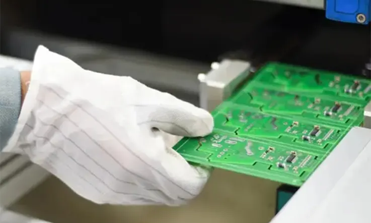
Design for Manufacturing (DFM) is a critical consideration when placing a PCB order and can affect the success of your manufacturing process. It’s important to avoid incorporating features in your circuit board design that could complicate the assembly process as it could result in additional production costs and wastage. If you have designed a PCB that is more complex than usual, it’s advisable to submit the files to your fabricator for evaluation before finalizing your order. This will allow you to identify any obstacles that may cause production delays or complications.
To ensure a seamless production process, it’s essential to anticipate and address potential problems well in advance. A comprehensive DFM assessment can help you evaluate the impact of specific design decisions and modify them if necessary to optimize manufacturability. The ultimate goal of this process is to ensure that your PCB design is optimized for manufacturing, allowing for a smooth and uninterrupted production process without any issues.
What Is Design for Manufacturing ?
Design for Manufacturing (DFM) or Design for Fabrication (DFF) is a critical engineering practice that focuses on designing products that facilitate the manufacturing process and reduce associated costs. When developing product designs, designers consider the actual capabilities of the manufacturing process, which involves analyzing designs to ensure they meet the requirements specified by the manufacturing process.
DFM is not limited to specific products since it can benefit any product, whether small or vast, simple or complex. For this purpose, we will concentrate on DFM in the context of electronic manufacturing, particularly Printed Circuit Board (PCB) DFM.
In electronic manufacturing, DFM is an essential concept, predominantly in maintaining competitiveness and minimizing costs. Manufacturers must optimize every stage of the production process, including manufacturing, to remain competitive in today’s highly competitive market. Electronics innovation is progressing rapidly, and companies need to launch new products continually. Inadequate DFM can result in pre-production faults that delay production and increase costs, causing significant setbacks that no electronics manufacturer can afford.
Why Is DFM a Crucial Part of the PCB Design Process ?
During the early stages of circuit board prototyping, functionality is typically prioritized over buildability. However, this approach can increase the cost of assembly if component placement is not optimal. To avoid these issues, PCB designers should consider automated manufacturing when designing the board and take steps to save costs on manufacturing expenses, even during small-scale production runs.
The inherent issues with prioritizing functionality over buildability become more apparent during the production phase. Components that are not located in a manufacturing-friendly manner may need to be repositioned to prevent the cost of manual assembly, which can drive up production costs and cause delays. Components that are not chosen for production over extended periods of time may also present manufacturing difficulties, such as high cost or limited supply.
While these issues are typically resolved during new product introduction (NPI), they can introduce additional challenges for PCB development. Modifying sensitive components to make the board more manufacturable may compromise circuitry performance; therefore, extensive layout modifications to accommodate DFM may require a complete redesign and revalidation of the board’s performance.
To avoid these issues, PCB designers should adopt effective DFM methods during the circuit board design process’s early stages. This will reduce the need for adjustments in the future while preserving the layout of sensitive circuitry fine-tuned for prototype performance. PCB designers should also familiarize themselves with potential manufacturing issues, ensuring they’re not overlooked in the design process.
The Process of PCB DFM
● PCB Design, Footprint and Packaging: The Design for Manufacturing (DFM) process is critical in the early stages of electronic manufacturing. The design phase, in particular, is crucial since it sets the foundation for optimal PCB design. During this phase, designers should focus on creating a PCB design with appropriate packaging and footprint. The reason being, inappropriate packaging and footprint can lead to higher manufacturing costs and more time spent on assembly.
To maximize profits, electronic manufacturers must ensure that their PCB design has suitable packaging and footprint. Additionally, implementing better DFM in PCB manufacturing can assist businesses in maintaining high profit margins by reducing the cost of manufacturing and assembling their products. By optimizing the design, businesses can reduce time-to-market, increase product efficacy and performance, and increase the competitiveness of their offerings. Ultimately, better DFM practices in electronic manufacturing can have a significant impact on the bottom line and overall success of an electronic manufacturing business.
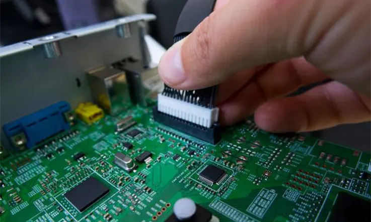
● Correct PCB Component Placement: The component placement phase holds significant importance in the Design for Manufacturing (DFM) process and constitutes the second step in electronic manufacturing. During this stage, components are placed on either the top or bottom side of the Printed Circuit Board (PCB) following placement rules, industry standards and guidelines. Proper routing of cables either on the top or bottom side, depending on the wiring standards, is also a crucial aspect included in this phase.
It is essential for designers to comply with placement standards, rules of thumb, and other similar guidelines while placing components on either the top or bottom side of the PCB. Such best practices assist in reducing manufacturing costs and assembly time while increasing the product’s profitability. Furthermore, improved DFM in PCB leads to lower production and assembly costs, enabling businesses to maintain high profit margins.
Inevitably, appropriately placed components and cables per industry standards can improve the PCB’s quality, reliability, and longevity while keeping manufacturing costs within optimal range. Therefore, electronic manufacturers must strive to achieve efficient and effective component placement during the PCB manufacturing process, starting with the DFM phase.
● Proper Wire Routing: In the Design for Manufacturing (DFM) process of Printed Circuit Board (PCB) development, the correct wire routing phase is the third and final step. After placing components on either the top or bottom side of the board as per wiring standards, designers focus on appropriately routing the wires to reach their destinations.
Proper wire routing plays a significant role in determining a PCB’s functionality, reliability, and longevity. Therefore, it is necessary for designers to route the wires strategically, in line with wiring standards and other similar guidelines.
Appropriate wire routing requires careful consideration of the location and quantity of components, as well as the signal and power requirements, to ensure proper current flow and signal integrity. Additionally, it is crucial to avoid routing wires in such a way that causes crosstalk, EMI, or other forms of interference.
Thus, it is essential for PCB design engineers to prioritize correct wire routing after placing components on the PCB, based on industry standards and wiring guidelines. Appropriate wire routing can result in improved product efficacy and performance, shorter production cycles and lead times, and lower manufacturing costs, which can ultimately enhance overall product quality and profitability.
PCB DFM: What Should be Reviewed ?
Printed Circuit Board (PCB) Design for Manufacturability (DFM) investigates all aspects of a PCB design that may impact its manufacturability, covering assembly, fabrication, flex/rigid-flex, microvia, panel, and substrate, among others. To reduce costs, DFM should also explore ways to position surface-mount technology (SMT) components and solder automatically. The Design for Manufacture process may follow either generic manufacturing standards or those of a specific company.
Given the complexity of the electronic manufacturing process, DFM operates in specific ways for different crucial phases within the PCB design-to-manufacturing workflow and beyond, ensuring the electronic product is produced correctly. This has led to the development of multiple subsets of DFM, each targeting a particular aspect of the manufacturing process.
● Design for Assembly (DFA) focuses on streamlining assembly procedures by reducing parts count, ease of handling, and utilizing standardized parts to increase assembly efficiency.
● Design for Testing (DFT) ensures that the design characteristics make the product easy to test for flaws that may impact its function.
● Design for Excellence (DFX) is a concept design phase that involves procedures, guidelines, and standards for producing high-quality products.
As such, PCB design engineers must integrate DFM, including DFA, DFT, and DFX, into the PCB design process to ensure upfront manufacturability assessments reduce both time and potential manufacturing costs while improving the overall product performance.

PCB DFM: When Should be Reviewed ?
DFM reviews are a crucial aspect of the PCB design and manufacturing process and can be conducted at various stages. However, in general, it is more advantageous to conduct DFM reviews during the design stage, particularly for new products. This practice is known as shifting to the left. The timing of the reviews is critical, as it is easier and less expensive to rectify potential issues at an early stage.
Conducting DFM reviews during the design stage allows for the production of more developed designs that can identify flaws and violations early on. This approach can prevent the wastage of significant time and material resources invested in flawed designs. Assessing a design early on also allows for optimization of production levels, such as high-mix, low-volume production, since the design remains flexible at that stage.
DFM reviews focus on potential fabrication concerns and may involve the assessment of design specifications, industry standards, fabrication tolerances, and other similar guidelines. By conducting DFM reviews during the design stage, the entire design and production process can be optimized to achieve better quality, functionality, and reliability, while reducing costs and lead times.
Therefore, as a PCB design engineer, it’s imperative to incorporate DFM reviews during the design stage with a specific focus on manufacturing and fabrication aspects. Early detection and rectification of potential issues through DFM reviews can save significant resources while optimizing production levels and improving the overall product quality.
How to Avoid: 5 Manufacturability Mistakes ?
In the field of PCB design layout, engineers may face the temptation to disregard certain aspects of the design that may seem unimportant at first glance. However, these components can be critical for ensuring that the design is manufacturable and failure to consider them can lead to significant consequences.
Similarly, customers may make a number of common mistakes when utilizing Design for Manufacturability (DFM), which can result in unfavorable outcomes. To ensure that your design is fabricated precisely, it is important to avoid these mistakes. With this in mind, we have compiled a list of typical errors and offer advice to help prevent them.
1. Not Engaging Your Supplier Early: It is strongly recommended that you involve your manufacturing vendor early in the PCB design process, ideally when you have a preliminary draft of the PCB layout.
Partnering with your vendor in this way can be beneficial as it can help identify minor design issues that may not have been apparent during the initial analysis of the PCB. Addressing these issues with the vendor before ordering components or submitting the design for certification approvals can help avoid costly and time-consuming rework.
By engaging your vendor as a collaborator in your PCB design, you are better equipped to troubleshoot and prevent problems, leading to a more efficient and effective production process.
2. Too Close to the Edge: It is important to maintain a specific distance between components and the edge of the PCB since having components placed too close to the edge can significantly increase the risk of failure. This is evidenced by instances where ceramic capacitors have been observed cracking when they were placed too close to the edge.
A skilled provider can easily detect this type of design flaw, and will likely request that the engineers involved make significant changes to the design. At a minimum, the supplier will request that the designers create routes around any parts of the board that are too close to the edge in order to avoid these issues.
3. Overstuffing the Board: If there are fewer components, then you won’t have to buy as many individual components. Because of this, there will be less of a requirement for:
● Testing
● Handling
● Processing
● Engineering
● Stock management
When using a lean design, leftover components and extra stock will almost completely disappear. There is no better indicator that anything is “manufacturable” than decreased prices and assembly times.
4. Overcomplicating Things: When designing a PCB, it is important to carefully consider the potential expenses associated with adding complexity to your design, such as incorporating surface mount technology (SMT) on both sides of the board. Such a design can result in significant additional costs and should be avoided wherever possible, except in rare cases where it is absolutely necessary. Similarly, drilling through holes on both sides of the board may also necessitate a second processing step.
It’s worth noting that using undersized components, while available, can pose challenges for contract manufacturers. Opting for the smallest size component when there is ample space on the board for a larger one can have a negative impact on the manufacturability of your product.
In order to facilitate fast and error-free production, it is advisable to invest extra time and effort in simplifying the design process in the early stages of the development process.
5. Unsuitable PCB Finish: Within the realm of PCB manufacturing, RoHS-compliant Hot Air Solder Leveling (HASL) has become the standard for applying finishes to components. However, this method of finish application is not ideal, as it completely removes any prior solder on the board.
As an alternative, Electroless Nickel Immersion Gold (ENIG) has become increasingly cost-effective. Comprised of a nickel layer followed by a gold coating, this finish yields a flat surface and superior solderability.
While assembly houses can handle ENIG finishes in-house, HASL orders must be outsourced to a third party.
It is important to regularly assess the possibility of switching to a different surface finish in order to realize potential savings in both time and resources during the manufacturing process.
How Does Design for Manufacturing Convert to PCB Layout ?
In the realm of printed circuit board (PCB) engineering, the principles of Design for Manufacturability (DFM) play a crucial role in ensuring that the PCB layout meets all required design specifications and functions properly regardless of size. When combining the components of a board into a smaller PCB, it can be challenging to fit them all into place and avoid issues such as acid traps and problems with edge clearance. This becomes even more challenging when designing a smaller PCB due to the reduced available space. The process of DFM can help identify and resolve these potential issues before putting the board into production.
Certified manufacturers use DFM engineering to examine the design of a circuit board to ensure that its dimensions are suitable for the functions it will perform and that it is capable of operating in the intended environment. For example, if the board is intended for use in high-temperature machinery, the PCB design must incorporate components and protective layers that can withstand these conditions.
The DFM process also involves testing the PCB design to ensure that it meets a set of standard requirements. If it does not meet these requirements, the approval for production will be withdrawn. If a PCB design fails easily under expected operating conditions, the designer may need to revise it with additional components to make it more capable of handling the tasks associated with the intended device.
DFM principles are critical in PCB fabrication and work in conjunction with design for fabrication, which addresses fabrication concerns and their application to PCBs.
How to Use PCB DFM Guidelines ?
One way to utilize the PCB Design for Manufacturability (DFM) checklist is to use it as a table of measures for each stage of the PCB development process. It is essential to periodically update the PCB DFM checklist to ensure that the same flaws do not reoccur on subsequent boards.
To facilitate easy assembly and manufacturing, it is crucial to determine the maximum number of components that can be placed on the PCB. It is also advisable to establish a consistent method for marking connections and components on the board to minimize the potential for errors during assembly. Any components that must remain undamaged during the assembling or manufacturing process should be clearly identified.
In addition to the above, a thorough PCB DFM checklist should cover a range of other design considerations, such as ensuring adequate spacing between components, managing trace widths and vias, addressing thermal management concerns, and verifying the electrical performance of the PCB. By following these guidelines, PCB designers can improve manufacturing efficiency and reduce the risk of costly mistakes.
It is crucial to use appropriate tolerances and add an extra margin to account for assembly faults or missing pieces that may occur. Accurate tolerances will prevent any issues during assembly or to the final product. It is vital to specify the hole size accurately for each component to avoid damage during the manufacturing or assembly process. It is also necessary to indicate the material that will be used for the construction of each individual component, such as polyimide or copper.
The required number of layers for a PCB design depends on the required components and how they will be interconnected. Therefore, it’s essential to specify the number of layers in your design. Additionally, it is important to test each component individually before sending them into production, particularly when working with SMT components. It is also recommended to verify that your design includes ground planes and that they are adequately connected to reduce electromagnetic interference.
Other important considerations include the selection of appropriate components, ensuring that there is sufficient space between the components, and supporting thermal management in consideration of the intended environment or operating conditions. The successful implementation of these recommendations will help streamline the production process and minimize errors.
Design Considerations for DFM
Design considerations for DFM (Design for Manufacturing) are the key factors that designers must consider during the PCB design process to ensure that the resulting design is optimized for successful manufacturing. Some of the critical design considerations for DFM are:
● PCB Layer Stack-up: Proper layer stack-up is essential in PCB design, and designers must ensure that they choose the correct number of layers for the board’s complexity and features. PCB layers should be arranged to minimize impedance mismatches, and all critical signals should be on inner layers to reduce susceptibility to electromagnetic interference (EMI).
● Component Placement: A well-planned component placement is important for DFM. Designers must ensure that components are placed correctly, with the appropriate orientation, size, and spacing. They should also consider the accessibility of components for assembly, test, and servicing purposes.
● Trace Routing: The routing of PCB traces is critical for DFM; designers must ensure that traces meet the minimum design rules in terms of width, spacing, and clearance requirements. The trace routing should be optimized for signal integrity, thermal performance, and EMI.
● Thermal Considerations: PCBs generate heat during use, and proper thermal management is essential to ensure long-term reliability. Designers must consider the thermal conductivity of the board material and ensure that components are placed in such a way that heat can be adequately dissipated.
● Manufacturing Tolerances: Designers must consider the tolerances of the manufacturing process during the design process. They should design the board to be within the allowable tolerances, preventing fabrication and assembly issues.
By carefully considering these DFM design considerations during the PCB design process, designers can maximize production yield, minimize the risk of fabrication and assembly errors, and ensure that the resulting PCBs are of high quality and reliability.
How Do PCB DFM Guidelines Work with DRC ?
Design rule checks (DRCs) are essential in detecting electrical flaws prior to the manufacturing of a printed circuit board (PCB). However, while DRCs provide a solid foundation for evaluating PCB quality, they are not capable of detecting every potential flaw. In contrast, the PCB Design for Manufacturability (DFM) guidelines provide a more comprehensive analysis, taking into account a greater variety of situations.
While DRC limitations can form the foundation for PCB design for manufacturing standards, DRC violations can point to design for manufacturing issues. Guidelines for DRC and DFM can be tailored to different aspects of the manufacturing process, such as design for fabrication (DFF) and design for assembly (DFA), respectively. In an ideal situation, checks should focus on the manufacture, assembly, and quality of the product.
Despite some similarities between DRC rules and DFM guidelines in terms of electrical component functionality, the latter is considered more comprehensive. Small disruptions in the flow of electricity can have cascading impacts on PCBs and the devices that contain them. As such, following the PCB DFM guidelines can save designers significant time and prevent design flaws from being overlooked during manufacturing.
Important of DFM in Printed Circuit Board Fabrication
PCB Design for Manufacturing (DFM) is the process of designing PCBs that are optimized for successful manufacturing. DFM involves designing the PCB with the manufacturing process in mind, considering the manufacturing capabilities and limitations of the PCB fabrication and assembly processes. The objective of DFM is to ensure that the final product meets the design requirements and specifications while minimizing the risk of manufacturing errors.
DFM is critical to the success of PCB production because it helps to ensure that the PCB can be manufactured and assembled with the required quality, reliability, and performance. By designing a PCB with DFM considerations in mind, designers can improve manufacturing yields, reduce the risk of failures during testing and operation, and reduce the overall cost of the PCB production.
Designing PCBs with DFM in mind can help to identify potential fabrication and assembly issues early in the design process, minimizing the risk of errors that could lead to production delays and added cost. Factors such as board size and shape, layer stack-up, component placement, trace routing, and thermal management are all critical design considerations for DFM.
Overall, DFM is essential for successful PCB production because it helps to ensure that the final product meets the design requirements and specifications while minimizing the risk of manufacturing errors. With proper DFM considerations, designers can improve manufacturing yields, reduce costs, and ensure the long-term reliability and performance of the PCB.
Conclusion
DFM Checks From JarnisTech: Provide One-stop Service for PCB Manufacturing and PCB Assembly
In order to ensure the reliability and compliance of PCB designs, it is necessary to obtain impartial and qualified third-party input during design inspections and compliance testing. JarnisTech Limited specializes in providing Design for Manufacturability (DFM) analysis services for PCB designs and prototypes to identify flaws and other issues.
Our team at JarnisTech Limited is equipped with the skills and expertise necessary to perform thorough DFM analysis of PCB designs and prototypes, helping to improve their function and reliability before moving forward with production. We invite you to contact us directly to learn more about how we can assist you in optimizing the quality and performance of your PCBs.


