
Ball Grid Array (BGA) technology is shaking things up in the PCB assembly world. This advanced assembly method lets you pack more punch into your designs, improve thermal performance, and boost electrical reliability. Ready to dive in? Let’s explore the ins and outs of BGA PCB assembly, ensuring you’re armed with everything you need to know, whether you’re a seasoned pro or just getting your feet wet.
What is BGA PCB Assembly?
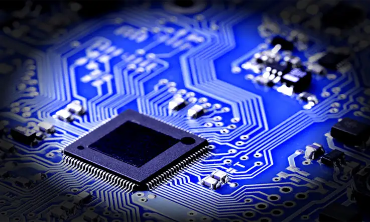
BGA PCB assembly is the process of mounting components on a printed circuit board using a unique configuration of solder balls placed in a grid pattern beneath the components. This method isn’t just a trend; it’s a practical solution that enhances the design of modern electronics. By utilizing these solder balls, manufacturers can maximize real estate on the board while ensuring reliable electrical connections.
BGAs are found in a wide variety of applications, from smartphones to complex automotive systems. Let’s dive into the nuts and bolts of BGA assembly to better understand its structure and processes.
Understanding the BGA Structure
To appreciate BGA assembly, we must first get familiar with the components that make up a BGA package.
Components of BGA Packages-
1.Solder Balls: These little gems serve as the connections between the component and the PCB. Each ball melts during the reflow process, creating a solid connection. Think of them as tiny anchors holding everything together.
2.Die: The semiconductor chip is where the magic happens. It’s the heart of the BGA, responsible for executing commands and processing information. This component is typically encapsulated in plastic or ceramic to protect it from physical damage and environmental factors.
3.Substrate: Acting as the backbone of the BGA package, the substrate provides mechanical support and electrical connections. It’s made of materials like FR-4 or ceramic, designed to withstand high temperatures during soldering while ensuring reliable performance.
BGA Assembly Process Overview
Now, let’s break down the BGA assembly process into manageable steps. Understanding these stages will give you a clear picture of how BGAs come to life.
1. Solder Paste Application-
The first step in the assembly process involves applying solder paste to the PCB pads where the BGA will be placed. Solder paste consists of tiny solder particles mixed with a flux medium, which helps facilitate the soldering process.
●Techniques: Common methods for applying solder paste include stencil printing and automated solder paste jetting. Stencil printing involves using a metal stencil that aligns with the PCB pads, allowing for precise application of solder paste. On the other hand, solder paste jetting is a newer technology that uses a jet to deposit paste directly onto the pads, providing a high level of accuracy—ideal for low-volume, high-precision applications.
●Tip for Success: Ensure the paste is evenly applied to avoid solder defects. A little care here goes a long way in achieving a reliable assembly.
2. Component Placement-
Once the solder paste is applied, it’s time to place the BGA component on the PCB. Precision is everything here.
●Automated vs. Manual Placement: Most manufacturers rely on automated pick-and-place machines for this stage. These machines use advanced vision systems to accurately position BGAs on the solder paste. Manual placement, while possible, can lead to misalignments, which can cause issues during the reflow process.
●Example: A manufacturer recently upgraded to a new pick-and-place machine equipped with advanced alignment features. As a result, they reported a 25% reduction in alignment errors, boosting their overall assembly efficiency.
3. Reflow Soldering-
This is where the real action takes place. The assembly is heated in a controlled environment to melt the solder balls, creating a solid connection between the BGA and the PCB.
●Reflow Techniques: The two main techniques are convection reflow and infrared reflow. Convection reflow uses hot air to evenly heat the assembly, while infrared reflow applies heat more directly.
●Temperature Profiles: Maintaining the right temperature profile during reflow soldering is a must to ensure reliable PCB connections. A standard reflow profile has four main stages: preheat, soak, reflow, and cooling.
| Phase | Temperature Range | Purpose |
| Preheat | 150-180°C | Gradually raises the temperature to avoid thermal shock. |
| Soak | 180-210°C | Allows the solder paste to activate before melting. |
| Reflow | 220-250°C | Melts the solder balls for strong connections. |
| Cooling | Below 150°C | Rapidly cools the assembly to solidify solder joints. |
●Quick Tip: Use profiling software to monitor temperatures during the reflow process. It’s like having a roadmap to ensure everything goes off without a hitch.
4. Inspection and Testing-
After reflow, the assembly undergoes inspection to ensure everything’s up to snuff.
●Visual Inspection: This step involves checking for visible defects, such as misaligned BGAs or excess solder.
●Automated Optical Inspection (AOI): Many manufacturers utilize AOI systems to automate this process. These systems provide rapid feedback, catching defects early on.
●X-ray Inspection: For a deeper look, X-ray inspection is essential, especially for BGAs, where solder joints are hidden from view. This method allows you to detect internal defects, ensuring that every connection is rock solid.
●Testing: After inspection, electrical testing methods like Boundary Scan Testing (BST) or In-Circuit Testing (ICT) can confirm that all components are functioning correctly.
Solder Paste Application
When it comes to BGA PCB assembly, the first step is applying solder paste, which is the foundation for getting strong, reliable connections between the board and the BGA component. Let’s break down the two most common techniques used in the industry, and see how they stack up.
Techniques for Solder Paste Printing
Stencil Printing-
This is the old reliable of solder paste application. Stencil printing involves using a metal stencil, precisely aligned with the PCB, to deposit solder paste onto the designated pads. It’s like using a cookie-cutter mold, but for paste. This method has been around for years and is perfect for high-volume runs where consistency is key.
●How It Works: A squeegee applies pressure on the stencil, pushing solder paste into the stencil apertures, leaving it only on the PCB pads.
●Benefits: Stencil printing is fast, cost-effective for large-scale manufacturing, and can handle multiple components in one go. But, it does come with a caveat: if the stencil or alignment isn’t perfect, you could end up with too much or too little paste, which might cause solder joint issues later on.
Jet Printing-
Now, if you’re looking for precision—especially on smaller production runs—jet printing is the slick alternative. Instead of relying on a stencil, this method shoots small droplets of solder paste directly onto the pads. Think of it as 3D printing for solder paste, but with laser-focused accuracy.
●How It Works: Jet printing uses a nozzle to place solder paste exactly where it’s needed, eliminating the need for a stencil altogether. This method is perfect for high-density PCBs where precision and control are necessary.
●Benefits: Jet printing allows for more flexibility. Since no stencil is required, you save on stencil costs and avoid issues with misalignment or stencil wear and tear. With jetting, you can adjust the paste volume whenever needed, which is a big win for prototypes or small-batch runs. This method is also a go-to for designs that are tight on space, where accuracy is a game-changer for making solid connections.
Case Study: Boosting Paste Printing Accuracy-
Let’s talk real-world results. Imagine a manufacturer dealing with inconsistent solder joints on their BGA assemblies. They were using traditional stencil printing and constantly had issues with too much or too little solder paste on certain pads. Enter jet printing—this company switched up their process, investing in high-precision jet printing for their PCB assemblies.
The outcome? A 30% boost in solder paste accuracy. This led to fewer assembly errors, lower rework rates, and faster production times. The switch not only cut down on wasted materials but also gave them a competitive edge in delivering high-quality electronics.
| Technique | Best For | Key Benefits |
| Stencil Printing | High-volume production | Cost-effective, fast, covers multiple pads at once |
| Jet Printing | Low-volume, high-precision applications | Flexible, no stencils needed, highly accurate paste application |
Why Does This Matter?
Both methods have their place in BGA PCB assembly, and choosing the right one can be the difference between a successful production run and troubleshooting solder issues all day. Jet printing may cost a bit more upfront, but if you’re running a precision-focused operation, it’s worth the investment. Meanwhile, stencil printing is still a go-to for mass production.
Component Placement in BGA PCB Assembly
Component placement is like threading a needle—you’ve got to be spot on, especially when dealing with BGA components. The challenge? BGAs are famous for their fine pitch and dense pin configuration, which means precision isn’t just recommended, it’s mandatory. Whether you’re rocking automated machines or going the manual route, each method has its ups and downs. Let’s dive in.
Automated vs. Manual Placement: The Showdown
Automated Placement: For any serious volume production, automated pick-and-place machines are the go-to solution. These machines are built to manage the intricate needs of BGA Assembly, using laser-guided accuracy and cutting-edge vision systems to ensure every component lands exactly on target. With their precise handling, cut down on placement errors and keep the process moving smoothly.
●How It Works: The machine grabs BGA components from a reel or tray and places them on the PCB, guided by smart vision systems that check for alignment down to the micron.
●Why It’s Preferred: Speed and accuracy. Automated machines can place thousands of components per hour, all while maintaining consistency. The days of worrying about misplaced BGAs causing electrical issues are long gone with these tech-savvy systems.
Manual Placement: Manual placement, on the other hand, is an option but comes with a few risks—especially if you’re working with BGA components. It’s a bit like playing darts blindfolded; you might hit the target, but it’s risky.
●How It Works: An operator uses tweezers or vacuum tools to place each component by hand, relying on visual inspection for alignment. While it might be okay for prototypes or very small runs, the risk of misalignment goes up.
●Challenges: Let’s face it—human error is real. Without automated assistance, precision is tough to guarantee, and a slight misalignment can cause major headaches down the line. This is why manual placement is usually reserved for small batches or prototypes.
Key Considerations for Accurate Component Placement
1.Pick-and-Place Technology: Automated systems use optical sensors and vision systems to ensure precision placement of BGAs. These machines are programmed to adjust positioning in real-time, making sure everything is aligned perfectly. They’re basically the sharpshooters of PCB assembly.
2.Fiducial Markers: Fiducial markers are like your GPS coordinates for the machine. These small metallic markings on the PCB provide reference points, helping the machine calibrate and adjust the placement process. This simple addition can be the difference between a flawless assembly and one that’s out of whack.
3.Nozzle Size and Type: The type of nozzle used in the pick-and-place machine matters, especially with BGA components. Too much force can damage the component, and too little won’t pick it up correctly. Think of it like finding the right size hammer—precision tools need precise handling.
Visual Aid: BGA Component Placement Diagram
Imagine a detailed diagram showing a BGA component being placed onto a PCB. The machine’s nozzle hovers, perfectly aligned with fiducial markers, while solder paste sits ready on the pads. Diagrams like this help engineers visualize the process and understand the exact level of precision required.
| Method | Best For | Advantages |
| Automated Placement | High-volume, high-density | Speed, accuracy, and repeatability |
| Manual Placement | Prototypes, small batches | Flexible but prone to human error, not ideal for BGAs |
Automated vs. Manual Placement
Let’s consider a real case study. A telecommunications company struggled with inconsistent manual placement of BGAs during their prototype phase. Misaligned components led to defective boards, costing time and resources to rework. They switched to automated placement and saw a 95% reduction in defects on their first production run. Not only did the automated machines save them time, but they also drastically cut down on rework, improving overall efficiency. The difference was like night and day.
Reflow Soldering: Heating Things Up the Right Way
When it comes to getting those BGAs properly attached to your PCB, reflow soldering is your go-to process. This is where the solder paste gets heated up and melted, creating strong connections between the BGA and the board itself. But here’s the kicker—reflow soldering isn’t a one-size-fits-all deal. Different methods and temperature profiles can make or break your solder joints, so let’s break it down and see how you can make sure your BGAs are locked in tight.
Reflow Techniques and Profiles: Getting the Heat Just Right
There are a couple of ways to tackle reflow soldering, and each has its perks. Whether you’re using convection or infrared methods, you need to keep your temperature profiles dialed in. If you overcook it, you risk damaging components. If it’s too cold, you might end up with weak solder joints. Let’s dive into the two main techniques used in reflow soldering.
1.Convection Reflow: This technique uses hot air to heat both the PCB and solder paste evenly. Think of it like an industrial-grade oven, circulating air to make sure every part of the board heats up at the same rate. It’s reliable, and it’s the go-to method for most high-volume production lines.
2.Infrared Reflow: If you need a more targeted approach, infrared reflow is where it’s at. Instead of blasting the entire board with hot air, this method uses infrared radiation to heat specific areas. While it can be more precise, it requires careful tuning to avoid uneven heating, especially with larger boards or components that vary in thermal mass.
Temperature Profiles: The Secret Sauce of Reflow
Just like you wouldn’t throw a steak straight onto a grill without preheating it, you shouldn’t jump straight to max temperature in your reflow process. Temperature profiling is all about hitting the right stages at the right time. Each step in the profile is designed to prepare the PCB and solder paste for perfect joint formation. Let’s take a walk through the process.
1.Preheat Stage: This is where things start off slow. The PCB is gently warmed up to avoid thermal shock. If you rush this stage, components can crack or warp. By gradually ramping up the heat, you allow the entire board to stabilize and prep for the higher temperatures ahead.
2.Soak Stage: Once the board is warmed up, it enters the soak phase. At this stage, the temperature sits steady enough to activate the flux in the solder paste, working to clean the metal surfaces and get them ready for a solid bond. Skipping this step or setting the wrong temperature can lead to weak joints that won’t hold up.
3.Reflow Stage: Now we’re in the main event. The temperature peaks just high enough to melt the solder paste, allowing it to flow and form solid joints between the BGA balls and PCB pads. But don’t get carried away—too much heat can cause bridging or voids, while too little leaves cold joints that don’t hold up.
4.Cooling Stage: Once the solder has done its thing, you’ve got to cool it down.Quick cooling keeps microcracks and other defects at bay, but move too fast, and you’re looking at possible stress in the joints. The goal is to find the sweet spot for cooling that locks your BGAs in place securely.
Troubleshooting Common Reflow Issues: Heads Up for Potential Pitfalls
Even with the best setup, things can still go sideways during reflow soldering. Here’s a quick look at some of the common hiccups and how to avoid them.
1.Solder Bridging: This happens when too much solder flows and creates a bridge between two pads. To avoid this, you want to keep an eye on your stencil design and make sure your reflow profile isn’t too hot.
2.Insufficient Wetting: If the solder doesn’t properly bond with the component or PCB, you’ve got yourself a weak joint. This usually comes down to not getting enough heat during the reflow stage, or your solder paste just isn’t cutting it.
3.Voids in the Joints: Voids are little pockets of gas that get trapped in the solder. They can compromise the strength of the joint, especially in BGAs. To prevent this, monitor your reflow atmosphere and make sure your profiles are dialed in. Using nitrogen during reflow can also help reduce oxidation, which leads to voids.
| Issue | Cause | Fix |
| Solder Bridging | Excess solder or overheating | Adjust stencil or reflow profile |
| Insufficient Wetting | Low reflow temperature or poor paste | Increase temperature or use better solder paste |
| Voids in the Joints | Trapped gas, improper reflow atmosphere | Optimize reflow atmosphere, use nitrogen |
Case Study: Solving Reflow Defects in Automotive Electronics
Let’s say you’re working with a top-tier automotive electronics manufacturer. They noticed that after reflow, their PCBs had issues with solder joint integrity. Upon investigation, they found that their temperature profiles were off—too much heat during the reflow stage led to solder bridging, while their cooling stage was too fast, causing microcracks. After tweaking their reflow oven settings and introducing nitrogen into the process, their defect rate dropped by 40%. Boom—problem solved.
Inspection and Testing: Catching Issues Before They Become Disasters
You’ve invested the time and precision to place and solder every BGA PCB Assembly. Now comes the final checkpoint before those boards are ready to roll out the door—inspection and testing. For BGAs, a deep dive is essential to catch any hidden issues that might be lurking under the surface. Here’s a breakdown of inspection methods that’ll ensure your boards come through flawlessly.
X-ray Imaging for BGA Inspection: Seeing Through the Surface
BGA components hide their connections underneath, which means visual inspection won’t cut it. This is where X-ray imaging steps up to bat. It’s like having X-ray vision—letting you spot defects that could otherwise go unnoticed until it’s too late.
Defect Detection Made Easy-
X-ray imaging is your go-to tool for identifying hidden issues like voids, solder bridges, or even missing solder balls. Unlike optical inspection, which only scratches the surface, X-rays let you peer deep into the solder joints, giving you a clear view of what’s really happening inside. Catching these problems early is a surefire way to prevent costly field failures down the line.
Real-Time Feedback in 2D and 3D-
Modern X-ray systems bring both 2D and 3D imaging to the table, letting you get a close look at each solder joint from various angles. With 2D imaging, you’ll get a clear and direct snapshot of each connection, while 3D imaging takes it a step further, offering a layered view that reveals details within the solder structure itself. Imagine spotting a small void in a joint before it sets off a whole chain of issues—keeping those connections in top shape, right from the start!
Case Study: How X-ray Inspection Slashed Failure Rates
Take this scenario: A military contractor, dealing with complex BGA assemblies, was experiencing an unacceptable rate of field failures. After digging into the root cause, they found that undetected solder joint defects were the main culprit. So, they added X-ray inspection to their process. The result? A whopping 40% reduction in failures. That’s a solid reminder that investing in advanced inspection pays off, especially when reliability is on the line.
| Before X-ray | After X-ray |
| High field failure rate | 40% reduction in failures |
| Hidden defects like voids went unnoticed | Early detection of solder defects |
| Costly product returns and repairs | Improved reliability and customer satisfaction |
Electrical Testing Methods: Putting Your Assemblies to the Test
Once your BGA PCB Assembly pass the inspection phase, it’s time to see if they’re ready for prime time. Electrical testing is the last checkpoint before your assemblies get out the door. Here are the heavy hitters when it comes to electrical testing for BGAs:
Boundary Scan Testing (BST)-
BST is a clever way to test the connections on your PCB without physically touching the board. Using the JTAG standard, this technique runs a test pattern through the components and checks for connectivity. It’s like sending a signal through a maze and seeing if it comes out the other side. If it doesn’t, you know where the problem lies. This method is perfect for detecting open circuits, shorts, and other connection issues that can be a pain to find.
In-Circuit Testing (ICT)-
ICT goes a step further, testing the electrical integrity of your board at multiple points. Think of it as a full-body checkup for your PCB. It ensures that everything from resistors to capacitors is doing its job. ICT uses physical probes to touch down on the board and verify that each component is operating as expected. If there’s an issue, ICT will catch it, giving you peace of mind before the product hits the field.
Optimizing BGA Assembly for Cost and Performance
Achieving an optimal balance between cost and performance in BGA (Ball Grid Array) assembly is like walking a tightrope—one wrong step, and you’re looking at budget overruns or a product that doesn’t deliver. Let’s look at how a few savvy choices in materials, techniques, and design can lead to cost-effective, high-performing BGAs without cutting corners.
Balancing Cost and Functionality in BGA Assembly
When budget is tight, it’s tempting to pick the lowest-cost options, but cheaping out on materials or skipping essential testing can invite headaches later. A better approach is to focus on cost-effective practices that also boost reliability.
Smart Material Selection-
Selecting the right solder paste and substrate can save on costs without compromising quality. For instance, using a high-reliability, no-clean flux paste minimizes extra cleaning steps, saving on labor and material expenses.
X-Ray Inspection for Quality Assurance-
Spotting issues early keeps your product on track and avoids rework down the line. By using X-ray inspection as part of your assembly process, you can detect voids, bridging, or misalignments early on. This type of inspection is especially useful for complex BGAs, where visual inspections alone won’t cut it. X-rays reveal what’s going on beneath the surface, ensuring a strong connection without blowing the budget.
Optimized Reflow Profiling-
Reflow profiling plays a huge part in solidifying the quality of each assembly, though it doesn’t always get the attention it deserves. Crafting a tailored profile for each assembly type prevents overheating and reduces the chances of weak solder joints. Precise control over temperature stages in the reflow process allows for stronger joints while avoiding excess thermal stress.
| Cost-Saving Strategies | Impact on Performance |
| No-clean flux paste | Reduces cleaning steps while preserving reliability |
| X-ray inspection | Identifies hidden flaws, boosting product durability |
| Reflow profile optimization | Ensures solder joint quality without excessive heating |
Design Considerations to Boost BGA Performance
Design choices are the backbone of BGA assembly performance. For the smoothest results, pay close attention to layout, signal integrity, and heat management. Fine-tuning each of these areas ensures every BGA connection is strong, stable, and ready for high-performance applications. Want your assemblies to perform without a hitch? Tackle these design elements head-on, and set yourself up for solid results.
1.Pad Layout and Spacing-
Your BGA’s pad size, spacing, and positioning determine how well it holds up over time. The trick is to ensure enough clearance between pads to prevent bridging but keep them close enough to avoid long lead lengths, which could introduce resistance and signal issues.
2.Signal Routing for Clean Performance-
Routing high-frequency signals away from BGA pads and placing ground planes strategically under the component helps reduce interference. This technique is especially useful in applications where signal integrity is a must, such as communications and computing devices.
3.Heat Dissipation and Power Integrity-
With high-performance devices, heat dissipation is a major consideration. Proper thermal vias, copper pours, and heat sinks improve heat flow away from the BGA. Managing heat reduces the risk of overheating, which can compromise the longevity of the solder joints and lead to field failures.
Example: An electronics manufacturer specializing in wireless communication found that by repositioning their ground planes and using optimized pad layouts, they reduced interference by 20% while cutting assembly costs by implementing automated inspection steps.
Design for Manufacturability (DFM) to Control Costs
Working hand-in-hand with your assembly partner to implement Design for Manufacturability (DFM) practices can yield cost-effective solutions. Adjusting the design to allow for automated assembly reduces both time and labor costs, a real win when scaling up production.
Example: For an automotive application, using a DFM approach led to design tweaks that allowed automated BGA placement and reflow inspection, reducing the overall cycle time by 15% and ensuring each board met strict quality requirements.
Challenges in BGA Assembly: Common Issues and Solutions
BGA (Ball Grid Array) assembly, while advantageous for high-density designs, brings its own set of challenges. The focus is on ensuring that the solder joints—where the real connections are made—remain reliable under various conditions. Let’s take a closer look at some common issues that can pop up in BGA assembly and how to keep them from ruining your day.
Solder Joint Reliability: Keeping It Together
When dealing with BGAs, solder joint reliability can make or break your product. Poor solder joints can lead to performance issues, early failures, or even total system shutdowns. The stakes are high because these joints are responsible for connecting the chip to the PCB.
Common Issues-
Some of the biggest culprits in unreliable BGA solder joints include incomplete reflow, voids, and poor wetting. Incomplete reflow happens when the solder paste doesn’t fully melt or flow correctly, leading to weak or intermittent connections. Voids—those pesky air bubbles trapped in the solder—can weaken the joint’s mechanical and electrical properties. Poor wetting, on the other hand, results in weak joints that don’t fully bond to the PCB pads.
Solution 1: X-ray Inspection
X-ray inspection gives you the power to see through the surface and spot hidden issues before they escalate. This non-destructive technique allows for detecting voids, misalignments, and incomplete reflow, helping you keep your solder joints intact. The best part? You can catch these issues early on, making sure your BGAs are good to go before they even leave the production line.
Solution 2: Controlled Reflow Profile
A smooth reflow process is all about nailing that temperature profile. Here’s how it breaks down:
●Preheat: Gently ramps up the temperature to prevent thermal shock.
●Soak: Evens out the heat across the board, allowing the flux to activate and prep the solder paste.
●Reflow: The peak temperature is where the magic happens—this is when the solder fully melts and creates a solid joint.
●Cooling: Rapid but controlled cooling solidifies the joint without introducing cracks or defects.
Keeping a close eye on each stage of reflow is the way to avoid unwanted defects. Using reflow profiling software helps you fine-tune each stage to prevent defects from creeping in. For instance, a manufacturer who had ongoing problems with weak solder joints fine-tuned their reflow oven’s profile, reducing their defect rate by 25%. Now, that’s something to write home about.
| Stage | Purpose | Common Issues Prevented |
| Preheat | Prevents thermal shock | Cracking, Delamination |
| Soak | Activates flux, evens out board temperature | Poor wetting, Inconsistent heat distribution |
| Reflow | Melts solder for joint formation | Voids, Incomplete Reflow |
| Cooling | Solidifies joints without introducing defects | Cracks, Solder Fatigue |
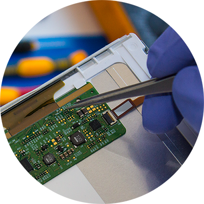
Repair and Rework of BGA Assemblies
When it comes to BGA (Ball Grid Array) rework, things can get a bit dicey. These little guys don’t like being tampered with too much, and reworking them requires a steady hand and the right tools. Whether you’re replacing a faulty BGA or fixing a bad solder joint, you’ve got to be careful not to damage the PCB or nearby components. Precision is everything here.
Challenges in BGA Rework: No Room for Error
Reworking BGAs comes with its own set of challenges. First, you’ve got the risk of overheating. Too much heat, and you could warp the PCB, cook nearby components, or even damage the BGA itself. On the flip side, if you don’t apply enough heat, the solder won’t melt properly, leaving you with poor joints that could lead to further failures. It’s a tightrope act.
One of the trickiest aspects of BGA rework is aligning the component perfectly back onto the pads once you’ve removed it. With hundreds of tiny solder balls under each chip, even a slight misalignment can spell disaster. And let’s not forget the cleaning process. After removing the BGA, those leftover solder remnants can cause issues unless they’re cleaned up properly. But don’t worry—there are effective ways to deal with these challenges.
Effective Rework Practices: Tools of the Trade
To make BGA rework as painless as possible, you’ll need the right tools and techniques. Here are the go-to methods pros use for successful repairs:
1.Reflow Hot Air Systems-
When you’re dealing with BGA rework, hot air systems are your best friend. These systems use precise, controlled heating to safely remove and replace BGAs. The trick is to apply just enough heat to melt the solder under the BGA without damaging other components on the board. Controlled airflow ensures that the heat is directed where it needs to go, allowing for smooth removal. Plus, these systems are designed to work with different PCB sizes and BGA packages.
Case Study: A telecommunications company faced consistent failures in their BGA assemblies due to faulty joints. They upgraded their rework setup to include a reflow hot air system, and their defect rate dropped by 35%. A bit of investment saved them a ton of headaches down the line.
2.Solder Wick for Clean-Up-
Once the BGA is removed, you’re left with solder on the pads that need to be cleaned up before reinstallation. Solder wick—sometimes called desoldering braid—is a copper braid that soaks up the excess solder when heated. It’s a quick and effective way to ensure the pads are clean and ready for the new BGA. Just apply some heat and watch the wick do its thing.
3.Precision Alignment Tools-
Getting the BGA aligned perfectly is a must. Precision alignment tools, often integrated into rework stations, help you position the BGA exactly where it needs to be. These tools use high-magnification cameras to make sure every solder ball lines up perfectly with its corresponding pad. One misaligned ball, and you’re in trouble—but with these tools, you’re good to go.
Best Practices for Success
Here are a few tips to keep in mind when reworking BGAs:
●Use Flux: Always apply flux to the pads before placing the new BGA. This ensures the solder flows evenly and bonds well.
●Monitor Temperature: Keep a close eye on the rework station’s temperature. Too hot, and you risk damaging the PCB; too cool, and the solder won’t reflow properly.
●Inspect with X-ray: After rework, use X-ray inspection to make sure the new joints are solid and free of defects like voids or misalignments.
| Rework Tool | Purpose | Outcome |
| Reflow Hot Air System | Safely remove and replace BGAs | Prevent overheating and damage |
| Solder Wick | Clean solder residue from pads | Ensure smooth, clean surface |
| Precision Alignment Tool | Align BGA with pads for reinstallation | Accurate, defect-free placement |
Why Precision Matters in BGA Soldering?
In high-precision applications, even the slightest misalignment or defect can affect the entire assembly. Here’s how precise soldering keeps everything tight:
●Uniform Heat Distribution: By controlling heat distribution with reflow or vapor phase soldering, you’re setting up each BGA for a perfect connection, ensuring every solder joint is robust and dependable.
●Minimizing Defects: Techniques like X-ray inspection and optical alignment tools allow for real-time monitoring, catching issues like misalignment, voids, or solder bridges early on. The fewer the defects, the better the overall performance of the board.
●Consistent Bonding: Proper soldering techniques allow BGAs to withstand temperature swings and physical stresses over time, essential for everything from consumer electronics to critical medical devices.
Practical Applications: Where BGA Precision Shines
Industries ranging from telecommunications to medical devices count on BGA soldering to power their innovations. Here’s a quick comparison of soldering techniques used across industries:
| Industry | Preferred Soldering Technique | Reason for Choice |
| Medical Devices | Controlled Reflow | High precision, reliable under stress |
| Aerospace/Military | Vapor Phase Soldering | Handles extreme conditions, thermal stability |
| Consumer Electronics | IR Reflow | Cost-effective, targets specific areas |
Why Choose Us?
The BGA Assembly Capability of JarnisTech
At JarnisTech, we pride ourselves on our top-notch engineering team and cutting-edge machinery, dedicated to delivering BGA packages that are both high-quality and precise. Our turnkey services encompass not just BGA assembly but a wide range of assembly methods tailored to meet diverse customer needs.
Advanced Equipment in SMT Assembly
Our fully automated SMT production line is designed to ensure high precision and maximum yield across all assemblies. Here’s a snapshot of our state-of-the-art equipment that keeps us ahead of the curve:
| Equipment Type | Description |
| Automatic Solder Dispensing | Ensures accurate solder placement for optimal joint formation. |
| Automatic Placement Machines | Guarantees precise component placement for assembly efficiency. |
| Reflow Ovens | Maintains controlled heating for perfect solder joint integrity. |
| X-ray Inspection Systems | Detects hidden defects in BGA packages for superior quality. |
| Automated Optical Inspection (AOI) | Verifies assembly integrity and checks for defects in real-time. |
BGA Process of Inspection
Inspecting BGA packages presents unique challenges due to solder balls being positioned beneath the chip. Traditional optical methods often fall short in revealing defects or cracks within the solder joints. To enhance detection accuracy in our SMT assemblies featuring BGA components, we employ a comprehensive mixed inspection technique that includes:
●Electrical Testing: Ensures connectivity and functional integrity.
●Boundary Scanning: Checks for electrical continuity without physical probing.
●Automated X-ray Inspections: Provides a non-destructive method to visualize solder joint quality.
By leveraging these advanced inspection techniques, we significantly boost the reliability of our assemblies.
BGA Capabilities for Assembly
Our automated BGA soldering processes are meticulously controlled to ensure quality and consistency. At JarnisTech, we specialize in designing and manufacturing BGA Assembly PCBs tailored to your specific needs. Our capabilities include:
Minimum BGA Pitch: We can accommodate pitches as tight as 0.25 mm.
Types of BGA Assembly Services:
●Micro BGA
●Micro Fine Line BGA (MBGA)
●Stack BGAs
●Plastic BGA (PBGA)
●Ceramic BGA (CBGA)
●Lead BGA and Lead-Free BGA
●Supported BGA Types
Here’s a comprehensive list of BGA types we support, ensuring a wide array of applications:
| BGA Type | Description |
| CABGA | Chip Array BGA |
| CTBGA | Thin Chip Array BGA |
| CVBGA | Very Thin Chip Array BGA |
| WLCSP | Wafer Level Chip Scale Packaging |
| FCBGA | Flip Chip BGA |
| FCmBGA | Flip Chip Micro BGA |
| LBGA | Low-profile BGA |
| BGA | Standard Ball Grid Array |
| DSBGA | Die-size BGA |
| FBGA | Fine BGA, mainly for systems-on-a-chip designs |
| LGA | Land Grid Array |
| CSP | Chip Scale Package |
With BGA assembly technology becoming commonplace, our extensive experience as a PCB manufacturer sets JarnisTech apart from the rest. We consistently deliver BGA assemblies that exceed industry standards, bolstered by rigorous quality control practices.
Choose JarnisTech for Your BGA Assembly Needs
If you’re looking for precision and quality in BGA assembly, JarnisTech is your go-to choice. Our experienced team and advanced equipment ensure that your projects are handled with the utmost care and expertise. Don’t compromise on quality—partner with us and elevate your PCB assembly experience today!
FAQ: BGA PCB Assembly
1. What are the advantages of using BGA in PCB assembly?
BGA packages allow for higher pin density and improved thermal performance compared to traditional packages. This is particularly beneficial for compact designs and high-speed applications. Additionally, the solder ball connections can reduce the risk of mechanical stress on the solder joints.
2. How do I choose the right BGA for my application?
Selecting the appropriate BGA package involves considering factors such as the size of the PCB, required pin count, thermal characteristics, and the specific application environment (e.g., automotive, consumer electronics, or aerospace). It’s also essential to consult with manufacturers to understand the specifications and compatibility of various BGA types.
3. What are the common defects in BGA assembly, and how can they be mitigated?
Common defects include solder bridging, voids, and insufficient solder. To mitigate these issues:
Use accurate solder paste printing techniques.
Ensure proper reflow profiles are set to avoid overheating or underheating.
Implement robust inspection methods like X-ray imaging to detect issues early.
4. Can BGA components be repaired or reworked?
Yes, BGA components can be repaired or reworked using specialized tools such as hot air rework stations. It’s essential to follow best practices for removal and replacement to avoid damaging the PCB or adjacent components.
5. How do I ensure the reliability of BGA solder joints?
Ensuring reliability involves:
●Implementing controlled manufacturing processes.
●Regularly testing and inspecting assemblies using X-ray and electrical testing methods.
●Selecting the right materials, such as high-temperature solder for critical applications.
6. What role does moisture sensitivity play in BGA assembly?
Moisture sensitivity is a critical factor in BGA assembly. Components exposed to humidity can experience defects like popcorn cracking during reflow. It’s vital to store moisture-sensitive devices in dry environments and consider baking procedures before assembly.
7. What types of testing should be conducted post-assembly?
Post-assembly testing should include:
●Electrical testing to verify circuit integrity.
●Mechanical testing to assess physical durability.
●Environmental testing to evaluate performance under various conditions.
Advanced PCB Assembly
PCBs We Can Assemble
- Min size: PCB whose width/length is less than 30mm should be panelized.
- Max size: single board 500mm*400mm | panel board 310mm*410mm.
- Layer Count: 1-60 layers (1-20 layers for mass production).
- Copper Thickness: 1/2oz – 17oz.
- PCB Types: Rigid PCBs, Flex PCBs, Rigid Flex PCBs, Rogers PCBs, Ceramic PCBs, etc.
- Surface Finishes: Lead/Lead-free HASL, ENIG, ImSilver, OSP, Gold plated, Immersion Gold, etc.
Components We Can Assemble
- SMT sizes: 01005, 0201 or larger.
- BGA pitch: 0.35mm or greater.
- BGA Ball count: 2 – 50.
- Fine pitch: 0.4mm or greater.
- WLCSP pitch: 0.35mm or greater.
- Components Height: 0.1mm – 12mm.
- BGA, micro-BGA, POP, CSP, LGA package, Flip chip, Hard metric connectors, Cable & wire, etc.
- Min. Components Spacing: 0.20mm for SMT parts, no specific demand for Thru-hole parts.
Custom PCB Assembly Capabilities
- Quick Turn.
- IPC III standard compliant.
- Prototype Quantities to Production Quantities.
- Single PCB Assembly and PCB Panel Assembly.
- Single and Double-sided PCB Assembly.
- Leaded Assembly, Lead-free or RoHS Compliant Assembly and No-clean Process Assembly.
- SMT Assembly, Thru-hole (DIP) Assembly, and Combo of SMT and Thru-hole Assembly.
- Consigned PCB Assembly, Partial consigned PCB Assembly and Full turnkey PCB Assembly.


