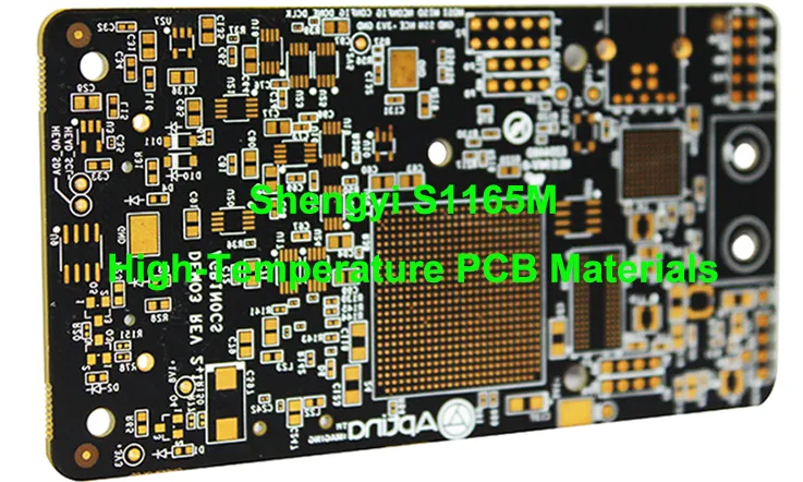
In the pursuit of next-generation electronics, selecting an advanced substrate like Shengyi S1165M is a foundational first step. However, the operational integrity of a high-performance printed circuit board (PCB) is not inherited from the raw laminate; it is forged through a doctrine of manufacturing precision. Transforming a material’s datasheet potential into its flawless execution within a final assembly hinges on the expertise, control, and discipline governing the fabrication process.
This text provides a comprehensive blueprint for converting Shengyi S1165M laminates into exceptionally reliable electronic assemblies. It moves beyond generalized descriptions to detail specific methodologies, advanced process controls, and collaborative design considerations that define high-reliability manufacturing.
Shengyi S1165M: A Foundation for Advanced Electronics
An objective analysis of Shengyi S1165M’s properties reveals its superior standing for sophisticated and demanding electronic applications. The full realization of these inherent attributes in a finished PCB is a direct function of the process engineering that follows—a core competency of specialized manufacturing services.
Achieving Unwavering Thermomechanical Stability
●High Glass Transition Temperature (Tg): With a Tg of approximately 165°C (DSC method), S1165M maintains its structural rigidity and dimensional stability at the elevated temperatures of modern lead-free soldering, which typically reach ~260°C. This property directly mitigates board warpage, twist, and component pad lift during assembly. The result is a high-yield, stress-free reflow process.
●High Decomposition Temperature (Td): A robust Td of approximately 345°C provides a crucial processing margin. The laminate’s chemical integrity remains intact through multiple high-temperature thermal excursions. Such excursions are required for multilayer lamination and component assembly, precluding irreversible material degradation and ensuring long-term durability.
●Low Z-Axis Coefficient of Thermal Expansion (CTE): S1165M exhibits a low CTE along its Z-axis, a determinant of interconnect reliability. As a board heats, the copper plating within vias expands. A high Z-axis CTE in the surrounding resin creates immense stress on the plated through-hole (PTH) barrel. The low CTE of S1165M minimizes this strain, drastically enhancing the intrinsic reliability of the interconnect and significantly reducing the probability of latent field failures due to via fatigue.
Table 1: Thermomechanical Properties of Shengyi S1165M
| Property | Value | Test Method |
| Glass Transition Temperature (Tg) | ~165°C | DSC |
| Decomposition Temperature (Td) | ~345°C | TGA |
| Z-Axis CTE (50°C – Tg) | ~55 ppm/°C | TMA |
| Z-Axis CTE (Tg – 260°C) | ~220 ppm/°C | TMA |
| T288 Time to Delamination | >10 minutes | IPC-TM-650 2.4.24 |
Leveraging Superior Electrical Characteristics
●Stable Dielectric Constant (Dk): The material offers a stable Dk across a broad spectrum of frequencies and operating temperatures. For engineers, this stability simplifies impedance modeling during CAM engineering. It allows for more accurate trace width calculations and yields higher first-pass success on controlled-impedance designs. A predictable Dk establishes the foundation upon which tight impedance tolerances can be guaranteed.
●Low Dissipation Factor (Df): S1165M possesses a low Df (nominally 0.012 at 1 GHz), making it an excellent substrate where minimizing signal attenuation is a primary design objective. The manufacturing process must be meticulously controlled to preserve this low-loss characteristic. This includes forming smooth copper traces and pristine dielectric interfaces to ensure the final board’s electrical performance precisely matches the material’s inherent potential.
Table 2: Electrical Properties of Shengyi S1165M
| Property | Value | Test Condition / Method |
| Dielectric Constant (Dk) | ~4.4 @ 1 GHz | IPC-TM-650 2.5.5.9 |
| Dielectric Constant (Dk) | ~4.2 @ 10 GHz | IPC-TM-650 2.5.5.9 |
| Dissipation Factor (Df) | ~0.012 @ 1 GHz | IPC-TM-650 2.5.5.9 |
| Surface Resistivity | >10⁸ MΩ | IPC-TM-650 2.5.17 |
| Volume Resistivity | >10⁹ MΩ·cm | IPC-TM-650 2.5.17 |
Identifying Target Applications for S1165M
Specifying Shengyi S1165M is a strategic engineering decision. It is indicated for devices where operational stability, signal integrity, and long-term endurance are non-negotiable design tenets. Proper fabrication ensures these benefits are fully realized in the final product.
Automotive and Industrial Control Systems:
In environments defined by continuous thermal cycling and mechanical vibration—such as engine control units (ECUs), industrial robotics, and factory automation hardware—S1165M’s thermomechanical robustness provides the long-term reliability needed to prevent interconnect fatigue. This ensures an extended, failure-free service life.
Telecommunications and Data Networking:
High-speed routers, switches, servers, and radio-frequency (RF) base station equipment demand substrates with stable electrical properties to maintain signal integrity at high data rates. S1165M offers a compelling performance-to-cost ratio for applications operating up into the 10-15 GHz range, providing a reliable platform for clear, high-speed data transmission.
High-Performance Computing and Data Servers:
The extreme thermal loads from modern CPUs, GPUs, and memory modules in densely packed server blades necessitate a substrate that withstands elevated operating temperatures without deformation. S1165M’s thermal stability meets these thermal management requirements, promoting system stability under heavy load.
Medical and Aerospace Electronics:
In high-reliability applications like diagnostic imaging systems, patient monitoring devices, and specific non-flight-critical aerospace systems, the substrate must provide an unwavering platform. The combination of S1165M’s intrinsic properties and a disciplined fabrication process delivers the level of assurance required for these applications.
The Fabrication Blueprint: A Doctrine of Precision
Translating an S1165M-based design into a physical, high-reliability artifact is a sequence of discrete, highly controlled technical processes. Adherence to this blueprint separates an exceptional outcome from a substandard one. This is the operational doctrine.
Executing Lamination and Press Cycle Control
The lamination stage fuses individual layers into a monolithic board. This process is particularly exacting for high-Tg materials like S1165M, and its perfect execution is a core manufacturing competency.
Material-Specific Press Cycles:
The S1165M resin system demands a unique temperature and pressure profile. Lamination presses utilize precisely engineered recipes. These involve a slow, controlled temperature ramp, a calculated dwell time at peak temperature to ensure full polymer cross-linking, and a controlled cooling phase to minimize internal stresses. This methodology prevents material degradation and yields a dimensionally stable final product.
Vacuum Lamination Integrity:
All S1165M multilayer boards are laminated under a hard vacuum. This process removes trapped air and volatiles from the resin matrix, resulting in a void-free dielectric structure. This step is fundamental to precluding delamination, improving CAF resistance, and ensuring the board’s long-term structural and electrical integrity.
Precision Layer-to-Layer Registration:
Advanced optical registration systems align the layers before pressing. All artwork is pre-compensated through a process known as scaling. This accounts for the specific, predictable shrinkage and movement of S1165M during the lamination cycle. This foresight ensures pads, vias, and features on all layers are perfectly aligned for subsequent drilling, maintaining a registration tolerance well within ±25µm.
Table 1: Key Lamination Process Parameters for S1165M
| Parameter | Typical Value / Range |
| Preheat Rate | 1.5 – 2.5 °C/sec |
| Peak Lamination Temperature | 190 – 200 °C |
| Dwell Time at Peak Temperature | 60 – 90 minutes |
| Vacuum Level Before Press Closure | <10 mbar |
| Cooling Rate (Controlled) | 2 – 3 °C/min |
| Registration Tolerance (Layer-to-Layer) | ±25 µm |
Performing Precision Mechanical and Laser Drilling
Drilling creates the Z-axis interconnects. An improperly executed drilling operation can introduce undetectable defects that lead to field failures.
1.Optimized Mechanical Drilling:
The S1165M glass-epoxy matrix necessitates specialized tooling. High-performance tungsten carbide drill bits with modified flute geometries are paired with calculated feed and speed rates to prevent resin smear and hole-wall damage. Strict hit-count limits are enforced for each drill bit, ensuring every hole is clean and precise.
2.Expert Laser Drilling for Microvias:
For High-Density Interconnect (HDI) boards, laser ablation parameters are tuned to the S1165M material. A precise recipe of laser power, pulse duration, and beam focus cleanly removes dielectric material without causing collateral heat damage or “resin recession,” ensuring a reliable foundation for microvia plating.
3.Advanced Post-Drill Hole Preparation:
After drilling, a multi-stage chemical or plasma desmear process is performed. This step removes any residual resin smear from the hole wall and micro-etches the dielectric surface. This texturing is a prerequisite for achieving a robust bond between the plated copper and the S1165M laminate, leading to highly reliable vias.
Table 2: Drilling and Hole Preparation Parameters for S1165M
| Parameter | Typical Value / Range |
| Drill Bit Material | Tungsten Carbide |
| Drill Speed | 80,000 – 120,000 RPM |
| Feed Rate | 1.0 – 2.5 mil/rev |
| Hit Count per Bit | ≤ 1000 hits |
| Laser Wavelength | 355 nm UV or 1064 nm IR |
| Desmear Method | Plasma or Alkaline Permanganate |
| Microvia Capture Pad Tolerance | ±25 µm |
Applying Advanced Plating and Etching
These steps define the final circuitry and govern both electrical performance and reliability.
1.Ductile and Uniform Copper Plating:
Plating a uniform layer of ductile copper inside high-aspect-ratio holes is a challenge. Advanced chemical baths and techniques like periodic pulse-plating are employed. This ensures uniform copper thickness throughout the entire via barrel, from the “knee” at the surface to the center. This uniformity allows the interconnect to withstand thermal stress without cracking.
2.Controlled-Environment Etching:
To create fine traces with high fidelity, automated, conveyorized etching systems with closed-loop control over chemistry, temperature, and pressure are utilized. This level of process control allows for reliably meeting trace width and spacing specifications, typically achieving a ±10% tolerance or better, a condition for predictable impedance control.
Table 3: Plating and Etching Control Metrics for S1165M Boards
| Parameter | Target Value / Range |
| Via Copper Thickness | ≥ 20 µm (center of barrel) |
| Surface Copper Thickness (Final) | 35 – 70 µm |
| Copper Ductility | ≥ 20% elongation |
| Etching Line Width Tolerance | ±10% |
| Trace/Space Capability | 75/75 µm (or better) |
| Plating Method | Pulse or DC Plating |
Applying Advanced DFM to S1165M Designs

A successful PCB originates from a design that comprehends the nuances of fabrication. A collaborative Design for Manufacturability (DFM) review aligns a design’s intent with the physical realities of the build process. For a material like S1165M, these DFM principles are fundamental.
Architecting the PCB Stackup
The stackup is the blueprint of the PCB. The objective is to ensure this blueprint is both high-performing and manufacturable.
●Material System Integrity: A multilayer stackup alternates S1165M cores with layers of S1165M prepreg. A foundational DFM requirement is to use prepregs from the same S1165M material system. Commingling materials can induce significant internal stresses during lamination, leading to delamination, warpage, or unpredictable electrical performance. This is verified at the start of every project.
●Strategic Weave Style Selection: S1165M prepregs are available in various glass weave styles (e.g., 106, 1080, 2116, 7628), each with direct manufacturing and electrical implications. A designer might choose a 106 weave for its smooth surface, yet the DFM process must account for its lower resin content, which is challenging when filling heavy copper topography. Collaboration helps specify a weave that optimally balances electrical needs with robust manufacturability.
●Intelligent Copper Weight Distribution: Selecting copper foil thickness requires balancing current capacity and etching resolution. Specifying heavy copper (≥2 oz / 70 µm) for a dense, fine-line signal layer is a DFM red flag, as it severely constrains etching reliability. An effective DFM strategy segregates power and signal functions onto layers with appropriate copper weights, ensuring both power integrity and signal fidelity.
Implementing Advanced Thermal Management
Modern electronics concentrate immense power into small footprints, making thermal management a primary design challenge. S1165M’s thermal stability provides an excellent starting point, but effective heat dissipation requires deliberate fabrication strategies.
Engineering Thermal Vias as Heat Conduits
●Thermal vias act as conduits, transferring heat from hot components to internal or external copper planes that function as heatsinks.
1.Design and Placement: DFM review analyzes the placement and density of thermal vias under high-power components. An effective design places a grid of vias directly under a component’s thermal pad. Guidance on optimal via diameter, plating thickness, and grid pitch can maximize thermal conductivity without compromising signal routing.
2.Fabrication Control: A thermal via’s effectiveness depends on a continuous, void-free copper plating barrel. Drilling and plating are optimized to ensure a thick, uniform copper wall (typically >25 µm). An available option is filling vias with thermally conductive epoxy and capping them (via-in-pad), which creates a flat, solderable surface and a highly efficient thermal path directly from the component’s solder joint.
3.Performance Impact: A well-executed array of thermal vias on an S1165M substrate can lower component operating temperatures by 10-20°C compared to a design without them. This translates directly to increased component longevity and system reliability.
Utilizing Heavy Copper Planes as Heatsinks
Internal and external copper planes are not just for power distribution; they are highly effective lateral heat spreaders.
●Heavy Copper Integration: Specialized processes exist for fabricating boards with heavy copper layers (3 oz to over 10 oz). Building with heavy copper on S1165M offers the dual benefits of high current capacity and exceptional heat spreading. The lamination process uses high-resin-content prepregs and optimized press cycles to ensure complete encapsulation of the thick copper features, preventing air voids that would impede thermal transfer.
●Plane Design Optimization: DFM analysis ensures power and ground planes are designed with maximal contiguous copper area under high-power regions. Maintaining large, unbroken copper planes maximizes the lateral heat-spreading capability of the board, drawing heat away from component hotspots.
Integrating Advanced Thermal Solutions
For extreme thermal challenges, more advanced solutions can be integrated directly into the PCB structure.
●Embedded Copper Coin Technology: This process embeds a solid copper coin into a cutout within the PCB. The coin can make direct contact with a component and extend through the board to an external heatsink. This creates a direct thermal path with much lower thermal resistance than vias alone. Fabricating this on S1165M requires precision milling and a specialized press cycle to bond the coin to the laminate, representing a high-level capability.
●System-Level Cooling Integration: A PCB design can be optimized for system-level cooling. This includes specifying locations for heatsink mounting holes and ensuring the board’s rigidity, enhanced by S1165M, can support the mechanical load of large cooling solutions.
Mastering High-Density Interconnect (HDI) with S1165M
HDI technology enables the miniaturization and improved performance of complex electronics. The dimensional stability and dielectric properties of S1165M make it an ideal substrate for such designs. Capable fabrication allows designers to harness the full potential of HDI.
Building the Foundation with Microvias
●Microvias are laser-drilled holes (typically <150 µm) connecting adjacent layers. They are fundamental to routing the dense I/O of modern packages like BGAs and FPGAs.
1.Precision Laser Ablation: UV and CO2 laser systems are calibrated for the S1165M resin and glass composition. A combination of techniques creates clean, well-shaped microvias with no residual debris or excessive heat damage. The resulting via shape is optimized for reliable copper plating.
2.Any-Layer HDI: Advanced HDI structures like every-layer interconnect (ELIC) are supported, where each layer has microvias. This provides immense routing flexibility, enabling dramatic board size reduction and shorter signal paths for better performance. The dimensional stability of S1165M is a requirement for maintaining registration in these high-layer-count builds.
Table 1: Microvia Formation Parameters for S1165M-Based HDI
| Parameter | Typical Value / Range |
| Microvia Diameter (Top) | 75 – 120 µm |
| Microvia Depth (1:1 Aspect) | ~60 – 100 µm |
| Laser Wavelength (UV) | 355 nm |
| Laser Power | 3 – 6 W |
| Registration Accuracy (Layer) | ±15 µm |
| Via Capture Pad Size | ≥150 µm |
Constructing Advanced Via Structures
The arrangement and type of vias are design elements in HDI.
●Stacked and Staggered Microvias: Both staggered microvias (offset on different layers) and stacked microvias (placed directly on top of each other) can be fabricated. Stacked microvias require a highly controlled sequential lamination and via-filling process but provide the densest routing solutions. The process ensures the via-fill copper is planar and void-free, providing a reliable base for the next microvia.
●Via-in-Pad Plated Over (VIPPO): VIPPO is a technique where a via is placed directly in the pad of a surface-mount component, filled, and plated over to create a flat, solderable surface. This is a method for escaping the dense pitch of modern BGAs. A controlled VIPPO process on S1165M boards ensures a planar surface, preventing solder defects and improving the thermal path away from the component.
Table 2: Advanced HDI Via Structures and Processing Metrics
| Parameter | Typical Value / Range |
| Microvia Stacking Tolerance | ≤ ±15 µm |
| Copper Via Fill Planarity | <5 µm step height |
| Electrodeposited Copper Fill | Voids < 1%, fully dense |
| VIPPO Flatness Deviation | ≤ ±10 µm |
| Lamination Cycles (Sequential) | 2–5 |
| Staggered Via Offset | ≥100 µm |
Enhancing Signal Integrity with Advanced Drilling
These techniques are employed to further enhance signal integrity in high-speed designs.
●Back-Drilling (Controlled-Depth Routing): In high-speed paths, the unused portion of a via barrel (the “stub”) can cause signal reflections. A controlled-depth drilling process after primary fabrication removes these stubs. Precision equipment can drill to a specified depth with tight tolerance (e.g., ±50µm), effectively eliminating the via stub and improving impedance matching for multi-gigabit signals.
Table 3: Back-Drilling Control Parameters for High-Speed S1165M PCBs
| Parameter | Typical Value / Range | Notes |
| Back-Drill Diameter | 0.2 – 0.4 mm | Slightly larger than original via to ensure full stub removal |
| Drilling Depth Tolerance | ±50 µm | Maintains stub ≤10% of signal rise time path |
| Residual Stub Length | <100 µm | Reduces signal reflections in multi-Gbps lines |
| Drill Bit Type | Controlled-depth CNC drill | Requires Z-axis servo precision |
| Post-Drill Cleaning | Mechanical + chemical clean | Removes burrs and debris for impedance continuity |
Preserving Signal Integrity: A Fabrication-Centric Approach
For high-speed designs, signal integrity (SI) is a primary consideration. Process choices can either preserve or degrade designed performance. SI preservation is a key manufacturing responsibility.
●Minimizing Conductor Losses: Signal attenuation relates directly to copper trace roughness. Standard copper foils are relatively rough to promote adhesion. For high-frequency applications, low-profile (LP) and very-low-profile (VLP) copper foils can be utilized with S1165M. The process must be optimized for these smoother foils, which significantly reduce conductor losses.
●Controlling the “Weave Effect”: At very high frequencies, the non-uniform fiberglass weave pattern can cause localized Dk variations, leading to timing skew in differential pairs. Engineering advice can include rotating the layout relative to the weave or selecting flatter, more uniform weave styles (like 2116 or 7628) to mitigate this effect.
●Ensuring Dielectric Uniformity: The lamination process is a determinant of a uniform dielectric constant. Any voids or resin-starved areas can alter the local Dk and impedance. Tightly controlled, vacuum-assisted lamination cycles ensure a homogenous, void-free dielectric medium.
●Executing Precision Etching: Over- or under-etching affects impedance and changes the trace’s cross-sectional profile. Automated etching processes create traces with sharp, well-defined trapezoidal profiles, minimizing signal distortion and reflections. This is validated through cross-sectional analysis.
Selecting and Applying High-Reliability Surface Finishes
The surface finish is the interface between the PCB and its components. The choice of finish and the quality of its application directly impact solderability, performance, and long-term reliability.
Electroless Nickel Immersion Gold (ENIG)
●ENIG is a common choice for its excellent planarity and solderability.
1.Process Control: The primary risk with ENIG is “black pad,” a hyper-corrosion of the nickel layer. A controlled ENIG line features tight management of bath chemistry, pH, temperature, and concentrations. An optimized phosphorous content in the nickel bath (typically 6-10%) resists corrosion, and gold thickness is carefully controlled to be protective but not brittle.
2.Best Use Case: Ideal for fine-pitch BGAs and other high-density components where surface planarity is needed.
Electroless Nickel Electroless Palladium Immersion Gold (ENEPIG)
●ENEPIG is often considered a “universal” finish, offering superior reliability.
1.The Palladium Advantage: ENEPIG adds a palladium layer between the nickel and gold. This layer acts as a robust barrier, preventing nickel corrosion. This eliminates the black pad risk and creates an exceptionally strong solder joint, suitable for gold and aluminum wire bonding.
2.Process Controls: An ENEPIG process should be a state-of-the-art, closed-loop system. The thickness of all three metal layers (e.g., Nickel 3-6µm, Palladium 0.05-0.15µm, Gold 0.03-0.05µm) is meticulously controlled.
3.Best Use Case: The ultimate choice for mission-critical applications where failure is not an option, such as in aerospace, medical, and high-performance telecommunications.
High-Temperature Organic Solderability Preservatives (OSP)
●OSP is a cost-effective, planar, and environmentally friendly option.
1.Formulation Matters: High-temperature OSP formulations are used, specifically designed to withstand multiple lead-free heat cycles without significant degradation.
2.Process Controls: OSP application is performed in a stringently controlled cleanroom environment. The process involves multiple cleaning and micro-etching stages to ensure the copper surface is pristine. This guarantees excellent wetting during soldering.
Validating Reliability: Stress Testing and Analysis
Datasheet values show potential; true reliability is proven under stress. A suite of rigorous testing methodologies validates that the fabrication process translates S1165M’s properties into a durable product.
Performing Thermal Shock and Interconnect Stress Testing (IST)
A prevalent failure mode is via fatigue from thermomechanical stress.
●Test Methodology: Representative test coupons are subjected to extreme thermal shock (e.g., -55°C to +125°C) for hundreds or thousands of cycles. Continuous four-wire Kelvin monitoring of daisy-chained interconnects through Interconnect Stress Testing (IST) detects minute resistance increases, signaling the onset of micro-cracking long before catastrophic failure.
●S1165M Performance Validation: In these tests, boards built with S1165M consistently outperform those made with standard FR-4. The material’s low Z-axis CTE, combined with a robust plating process, results in interconnects that endure significantly more thermal cycles, empirically validating both the material and the manufacturing quality.
Table 1: IST and Thermal Shock Test Conditions and Outcomes
| Parameter | Value / Range |
| Thermal Shock Temperature Range | -55°C to +125°C |
| Number of Cycles | 500 – 3000+ |
| IST Ramp Temperature | 25°C to 150°C |
| Interconnect Monitoring Resolution | < 0.1 mΩ (4-wire Kelvin) |
| Failure Threshold (Resistance Change) | ≥ 10% from baseline |
| Typical S1165M IST Cycle Endurance | > 1500 cycles |
Analyzing Conductive Anodic Filament (CAF) Resistance
●CAF is a latent failure mechanism involving the electrochemical migration of copper along the glass-resin interface, which can lead to short circuits.
1.The Threat Condition: High-density designs under high humidity and voltage bias are susceptible to CAF failures.
2.Rigorous Test Protocol: CAF resistance is evaluated by subjecting specialized test coupons to harsh conditions—typically 85°C, 85% relative humidity, and a sustained DC voltage bias—for over 1,000 hours. Insulation integrity is continuously monitored.
3.A Validation of Process Quality: The S1165M resin system is inherently CAF-resistant. However, this resistance can be compromised by a poor lamination or drilling process. Successful CAF testing is a powerful validation of process quality, proving a robust, sealed dielectric structure has been created.
Table 2: CAF Resistance Testing Parameters and Results
| Parameter | Value / Condition |
| Test Temperature | 85°C |
| Relative Humidity | 85% RH |
| Voltage Bias | 100 – 500 V DC |
| Test Duration | ≥ 1000 hours |
| Pass/Fail Criteria (Insulation Drop) | ≤ 1 order magnitude reduction |
| Typical S1165M CAF Performance | > 1000 hours, no failures |
Executing Rigorous Electrical Test Protocols
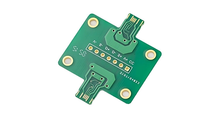
A fabricated PCB is not complete until proven electrically perfect. A multi-stage electrical testing strategy guarantees every board shipped matches the designer’s netlist.
Beginning with Netlist Extraction and Comparison
●CAD to CAM Verification: Upon receiving design files (Gerber/ODB++), CAM engineers extract a netlist. This CAD-generated netlist serves as the “golden reference.” A second netlist is generated from the final manufacturing tooling. These two netlists are digitally compared. Any discrepancy flags a potential data translation issue that is resolved before fabrication begins.
Conducting Bare-Board Testing
Two primary methods are used for 100% electrical testing of unpopulated boards.
●Flying Probe Testing: For prototypes and low-to-medium volume, flying probe testers are utilized. These machines use moving probes to contact every net, systematically checking for continuity and isolation. They require no custom fixtures, making them fast and cost-effective for small batches.
●Bed-of-Nails (Fixture) Testing: For high-volume production, a custom bed-of-nails fixture is built. It contains spring-loaded pins corresponding to every test point. The board is pressed onto the fixture, and all nets are tested simultaneously, making it extremely fast for mass production.
Performing High-Voltage (Hipot) Testing
For certain applications, Hipot (High Potential) testing is performed to verify the dielectric strength of the S1165M laminate.
●Test Protocol: This test applies a high voltage (e.g., 500V or 1000V DC) between conductors. The test measures leakage current. A successful test shows negligible leakage, proving the insulation can withstand the specified voltage without breakdown.
The S1165M Value Proposition: A Performance and Cost Analysis
Selecting a laminate requires a methodical analysis of performance, cost, and manufacturability. This analysis balances performance requirements against build complexity and total project cost.
Performance Upgrade: S1165M vs. Standard FR-4
●Reliability as a Driving Factor: For any product undergoing multiple lead-free reflow cycles or destined for a high-temperature environment, upgrading to S1165M is a prudent engineering decision. This choice increases the probability of a high-yield assembly process and reduces the likelihood of costly field failures.
●Signal Performance as a Driving Factor: For designs with high-speed interfaces (e.g., PCIe, DDR5), the lower Df of S1165M provides more performance margin. Furthermore, tight impedance control is more reliably achieved on S1165M, resulting in a board that performs closer to simulation.
●Calculating the Total Cost of Ownership: While S1165M has a higher initial material cost, it often yields a lower total cost of ownership. This calculation factors in the reduced costs from higher assembly yields, less rework, fewer field returns, and greater long-term product reliability.
Cost-Benefit Analysis: S1165M vs. Premium RF Materials
●Performance Threshold: For the most demanding high-frequency applications (e.g., mmWave), premium materials like Rogers or Megtron 6 offer even lower dielectric loss. S1165M is a capable and cost-effective solution for most applications up to the ~10-15 GHz range. An analysis of a design’s signal loss budget determines the point at which a premium material’s added performance justifies its significantly higher cost.
●Manufacturability and Lead Time: A core advantage of S1165M is that its fabrication follows a well-understood, high-Tg FR-4 process flow. Premium RF materials often require specialized handling that increases both cost and lead time.
Engineering in Action: S1165M Fabrication Case Studies
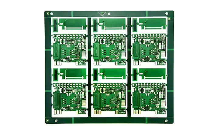
Theory is one thing; results are what matter. The following illustrates how these principles solve real-world engineering challenges.
Case Study 1: High-Density Consumer Electronics Motherboard
●The Challenge: A client was developing an ultra-slim laptop requiring a 12-layer motherboard with multiple fine-pitch BGAs and a high-speed LPDDR5 interface. Constraints included a 1.0mm thickness, a 100Ω differential impedance requirement, and survival of a 265°C double-sided reflow process.
●The Engineering Solution: A DFM review led to a re-engineered, perfectly symmetrical stackup to eliminate warpage risk. The new stackup used three thin S1165M cores and a precise combination of 106 and 1080 style prepregs. This met the thickness target and dialed in the dielectric height for impedance. A VIPPO process was implemented to accommodate the dense BGA breakouts.
●The Outcome: Final boards exhibited exceptional flatness (warpage < 0.5%). Time-Domain Reflectometry (TDR) testing confirmed impedance was controlled within ±7%. The client’s assembly house reported a first-pass yield exceeding 99%, a testament to the board’s thermal stability and manufacturing precision.
Case Study 2: Robust Industrial Robotics Control Unit
●The Challenge: A robotics supplier required a control board for a 10-year service life in a harsh automotive plant, with constant vibration and temperature swings (-20°C to 95°C). Preventing interconnect failure was the main concern.
●The Engineering Solution: S1165M was selected for its low Z-axis CTE and high Tg. The DFM review recommended increasing internal plane copper to 2 oz, which improved thermal dissipation and added rigidity. DFM software identified and replaced over 200 sharp 90-degree trace corners with 45-degree angles to distribute mechanical stress.
●The Outcome: Final assemblies were subjected to rigorous qualification, including a sine-on-random vibration test and 1500 thermal cycles. Post-test microsectioning analysis confirmed zero evidence of via barrel cracking or other fatigue-related failures, giving the client full confidence for mass deployment.
A Commitment to Quality Beyond the Standards
Adherence to standards is the baseline, not the ceiling. While operations can be certified to ISO 9001:2015 and boards built to IPC-A-600 Class 2 or Class 3, a commitment to quality runs deeper.
●Integrated Quality Management: Quality is embedded in every process. Statistical Process Control (SPC) is utilized at lamination, drilling, and plating to monitor stability and preemptively address deviations.
●Advanced Inspection Technology: Investment in state-of-the-art equipment allows for inspecting what the naked eye cannot. This includes Automated Optical Inspection (AOI) for every inner layer, 3D X-ray inspection for registration, and TDR for impedance verification.
●In-House Reliability Lab: An on-site microsectioning lab allows for rapid analysis of hole wall quality, plating thickness, and layer registration. This capability supports process control, first-article inspection, and root cause analysis.
●Full Lot Traceability: A comprehensive traceability system allows a finished PCB to be traced back to the specific laminate batch, machine operators, process parameters, and fabrication date. This is fundamental for process control and accountability.
Qualities of a High-Performance S1165M Fabricator
Choosing a fabrication service for a material like S1165M is a decision that impacts project success, timeline, and budget. The following are qualities of a suitable choice:
●Material-Specific Expertise: The service must not just process S1165M, but understand it. Process engineers should have optimized workflows for the nuances of high-Tg, low-loss materials, ensuring properties are enhanced, not compromised.
●Collaborative DFM Partnership: The service should act as an extension of an engineering team. A detailed, proactive DFM review optimizes a design for manufacturability, reliability, and cost-effectiveness.
●Investment in Technology: From vacuum lamination presses and laser drilling systems to advanced plating lines and inspection tools, the PCB fabricator must have invested in the capital equipment necessary to execute complex S1165M designs with precision.
●A Proven Track Record: A history of successfully delivering high-reliability S1165M boards for demanding applications across various industries is a strong indicator of capability. What is delivered is not just PCBs, but confidence.
Frequently Asked Questions (FAQ) about S1165M Fabrication
1.What is the typical lead time for an S1165M prototype project?
Lead time depends on layer count and complexity, but a typical 6-10 layer S1165M prototype is often completed within 8-12 working days. A precise quote can be provided upon review of a data package.
2.What data is needed for a quote and DFM review?
A complete data package is ideal. This includes Gerber or ODB++ files, a fabrication drawing specifying S1165M and other requirements, a stackup diagram, and a drill file.
3.Can hybrid stackups using S1165M with other materials be handled?
Yes, experience with hybrid builds, such as combining S1165M cores with Rogers materials for specific layers, is available. This requires careful DFM and specialized processing.
4.How is specified impedance tolerance guaranteed?
Impedance is guaranteed through a multi-faceted approach: using manufacturing-based stackup models, precise etching and lamination control, and final validation with TDR test coupons included on every production panel. A TDR report can be provided with the shipment.
5.What type of laser is recommended for drilling microvias in S1165M?
A UV (ultraviolet) laser is preferred for drilling microvias. It creates cleaner holes with less thermal damage than a CO2 laser, enabling finer features.
6.Is there a practical maximum layer count when fabricating with S1165M?
Boards with over 30 layers are reliably fabricated. Higher counts (40+) are achievable but demand rigorous engineering and process control.
7.What is the moisture sensitivity of S1165M, and how critical is baking before assembly?
The material is hygroscopic (absorbs moisture). Baking boards before assembly (e.g., 4-6 hours at 125°C) is highly recommended if they have been exposed to ambient humidity to prevent reflow defects.
8.At what signal speed or frequency should a designer consider upgrading from standard FR-4 to S1165M?
Consider upgrading from standard FR-4 when operating at frequencies above 1-2 GHz. S1165M is a cost-effective choice for applications in the 3-6 GHz range requiring good signal integrity.
Initiating a High-Performance Project
The successful fabrication of a high-performance PCB is the expression of synergy between advanced material science and disciplined process engineering. Shengyi S1165M provides the foundation; expert application of PCB manufacturing doctrine brings its potential to life.
A superior product that meets electrical specifications and embodies a level of physical integrity that defines market leadership is achievable. The process begins with these steps:
1.Secure Design Data Submission: Upload the complete fabrication data package, including Gerber/ODB++ files and a detailed fabrication drawing, through a secure portal.
2.Comprehensive DFM Review: An engineering group initiates a thorough DFM review, analyzing the design against the specific capabilities of the S1165M process.
3.Transparent Quotation & Feedback: A detailed quotation is provided, along with any DFM feedback, which may include suggestions for stackup optimization or design adjustments to enhance manufacturability.
Contact Jarnistech’s engineering team to discuss your S1165M project requirements and discover how fabrication expertise can become a competitive advantage.

