The copper layers embedded within a PCB function as pathways for electrical current, underscoring the importance of selecting an optimal copper thickness to ensure the assembly’s performance is not detrimentally affected. A comprehensive grasp of the relationship between copper weight, its efficacy in signal transmission, and the implications for PCB manufacturing costs is essential.
It is important to recognize that the chosen copper weight can significantly impact the overall PCB assembly fabrication process. Therefore, by providing a concise explanation of this relationship, designers can make well-informed decisions that strike the best balance between signal transmission needs and the practical considerations of PCB fabrication.
What Is PCB Copper Weight/Copper Thickness?
PCB copper weight, alternatively termed as copper thickness, signifies the amount of copper layered on a printed circuit board (PCB) within a specified region. Usually represented in ounces per square foot (oz/ft²) or micrometers (μm), this variable acts as an indicator of the thickness of the copper course bonded to the PCB’s exterior during the production phase.
Common copper weights seen in PCBs comprise 1 oz/ft² (approximately analogous to 35 μm), 2 oz/ft² (equivalent to circa 70 μm), and 3 oz/ft² (corresponding to around 105 μm). Additional variations can be accommodated based on explicit needs. The choice of copper weight hinges on the unique application and the design prerequisites of the PCB. Greater copper layers are often chosen for situations necessitating escalated current capacity or improved thermal management.
While in the PCB design phase, the contemplation of copper weight becomes integral as it influences the fabrication process and governs factors such as signal fidelity, impedance management, and heat dissipation capacities. Adopting diverse copper weights might imply the need for alterations in the PCB layout, encompassing detail changes to trace widths and the establishment of custom-made thermal handling strategies, thereby ensuring the circuitry’s highest functionality and long-term endurance.
The Role of Copper Weight in PCB Fabrication
The capacity of a Printed Circuit Board (PCB) to conduct current is intrinsically attributed to the thickness of the copper layer and trace. Certain critical aspects necessitate evaluation during the design process of the PCB, including the appropriate trace width for impedance-controlled boards, the total weight of the PCB, connector varieties suited for mounting on the board, and compatibility with numerous components. This evaluation supports the determination of optimal copper thickness settings.
The conductive nature of a PCB is fundamentally tied to the weight of its copper layer; an increase in copper weight results in enhanced conductivity and adds to the aggregate thickness of the circuit board. Therefore, a carefully calculated approach to copper thickness during the design stage is crucial, as alterations in thickness and width profoundly impact the board’s current carrying capability.
Furthermore, copper’s occurrence on the board bolsters its resilience against variable conditions. Industrial applications heavily rely on high-copper-weight PCBs, with several aerospace and defense industry products mandating their use. The reinforced copper weight in distinct circuit layers grants additional protection for the board, while copper-plated vias expedite the passage of high currents through the board, alongside enabling proficient heat irradiation towards an external heat sink.
In conclusion, copper thickness consideration is vital in PCB design due to its significant contribution to board’s current carrying capacity, conductivity, and durability. A comprehensive awareness of these elements is indispensable for the creation of a superior quality PCB tailored to match the unique requirements of its application.
Copper Weight/Copper Thickness Standards and Guidelines
Within the sphere of Printed Circuit Board (PCB) production, the measurement of copper weight or thickness is conventionally articulated in terms like ounces per square foot (oz/ft²) or micrometers (µm). And here Several primary standards and guidelines stipulate the designation of copper weight or thickness in PCBs:
IPC-6012B: A salient standard within this set is the IPC-6012B, crafted by the Institute of Printed Circuits (IPC), prescribes the prerequisites for rigid PCBs, encompassing pertinent stipulations about copper thickness. It segregates copper thickness into three precise categories: Class 1 (1oz/ft²), Class 2 (2oz/ft²), and Class 3 (3oz/ft² or higher). These divisions present a structured methodology for opting the fitting copper thickness for a PCB, ensuring it is bespoke to align with the stipulations of its proposed use.
MIL-PRF-31032: This is a military regulation that expresses requirements for printed circuit boards which includes copper thickness directives, indicated in ounces per square foot.
UL 796: This safety rulebook for printed wiring boards furnishes the minimum copper thickness necessary for several current-carrying capacities, providing guidance ranging from 0.5oz/ft² up to 10oz/ft².
NASA-STD-8739.4: A standard established by NASA, describing the specifications for fabricating rigid PCBs while setting various copper thickness levels for differing applications, from 0.5oz/ft² through to 6oz/ft².
JEDEC JESD 201: A directive from the Joint Electron Device Engineering Council (JEDEC), presenting requirements for printed wiring boards, furnishing advice on the lowest copper thickness over a spectrum of current-carrying capacities, from 0.5oz/ft² to 10oz/ft².
IPC-2152: This standard delineates a method for ascertaining the current-carrying prowess of PCB traces and vias based on their dimension and copper weight, incorporating charts and equations for computing current capacity per copper weight and trace/via dimensions.
IEC 60169-16: An international guideline stipulating the design and performance necessities for RF and microwave PCBs, it comprises copper thickness advice rooted in frequency range and signal power.
Importance of PCB Copper Thickness (Copper Weight)
The criticality of copper thickness to the performance and durability of printed circuit boards (PCBs) is profoundly substantial. Here are some core elements underlining its significance:
Efficiency in Signal Transmission: Ensuring an adequate level of copper thickness is crucial for fostering efficient signal transmission and reducing signal attenuation or deterioration. Greater thickness in copper traces encourages diminished resistance, enriched conductivity, and superior signal integrality, especially imperative for high-velocity and high-frequency functions. This aspect helps maintain ideal impedance levels and reduces the cross-talk among neighboring traces.
Power Dissipation and Thermal Management: High copper thickness layers demonstrate augmented current carrying capabilities, integral for accommodating significant electrical power transferences without substantial voltage reductions or excessive heat generation. This feature is particularly important for instances entailing high current flows across the PCB, like power electronics. An enhanced copper thickness promotes uniform heat dispersion, prevents heat clustering, and strengthens circuit dependability.
Mechanical Rigidity: The mechanical sturdiness of a PCB is greatly affected by its copper thickness. Increased copper layers contribute to the rigidity of the board, reducing the probability of deformation or bending during manipulation or during thermal cycling. In addition, it fortifies the structural integrity of plated through-holes, defending against barrel cracks or malfunctions.
Enhanced Durability: Increased copper thickness serves to safeguard the PCB against recurrent thermal cycles, elevated temperatures and environmental stressors. It provides better resistance to issues such as solder joint fatigue, oxidation and contamination, therefore extending the PCB’s endurance and dependability under strenuous circumstances.
Implications in Manufacturing: The selection of copper thickness also bears an impact on the PCB manufacturing process itself. Thicker copper necessitates longer etching periods and influences the precision of trace width and spacing. Striking a balance among the desired copper thickness, manufacturing limitations, and cost considerations is of utmost importance.
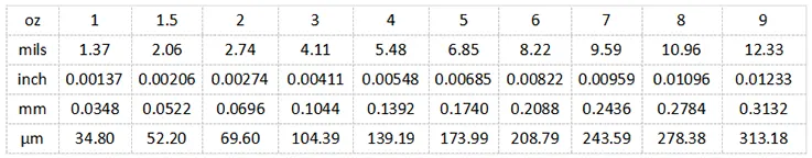
Copper Thickness Conversion Chart
Factors Affecting Copper Weight/Copper Thickness
Unique elements crucial to the performance and design of printed circuit boards (PCBs) fundamentally influence the copper weight or thickness, including:
Current Carrying Potency: The inherent ability of a PCB trace to transmit current correlates intimately with the thickness of the copper layer. Essentially, applications that require a heightened flow of current call for the utilization of more substantial copper layers.
Heat Regulation: Copper’s role is vital in managing the heat produced by the electronic components on the PCB. The facilitation of improved thermal regulation and the capacity to endure higher temperatures is achieved by more pronounced copper layers.
Design Directives: Specific design facets, incorporating high-power traces, ground planes, and efficient heat management, may necessitate the need for escalated copper thickness.
Manufacturing Aspects: The technique employed to manufacture the PCB can impact its copper weight. Crucial factors include the initial density of the copper foil used and the thickness added during the plating process.
Cost Outcomes: The total expenditure in manufacturing a PCB correlates directly to the amount of copper used. As such, using thicker copper layers leads to heightened production costs.
Spatial Restrictions: Physical or design constraints on the PCB may limit the permissible use of copper, thus affecting the maximum feasible copper thickness.
Surface Completion: The selected surface finish for the PCB can affect the adhesive properties of the copper layer, which may, in turn, influence the optimal copper thickness.
Signal Fidelity: With high-frequency signal applications, the thickness of the copper layer can substantially affect signal integrity and potentially lead to signal reflections and crosstalk.
Material Qualities: The traits of the base material may require alterations in copper thickness to retain signal integrity. This is especially pronounced in materials with a high dielectric constant.
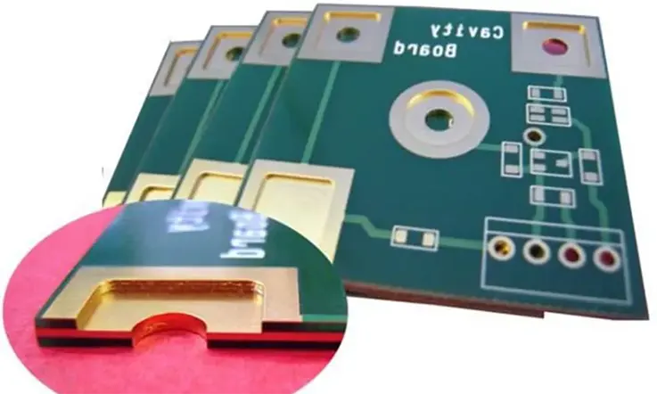
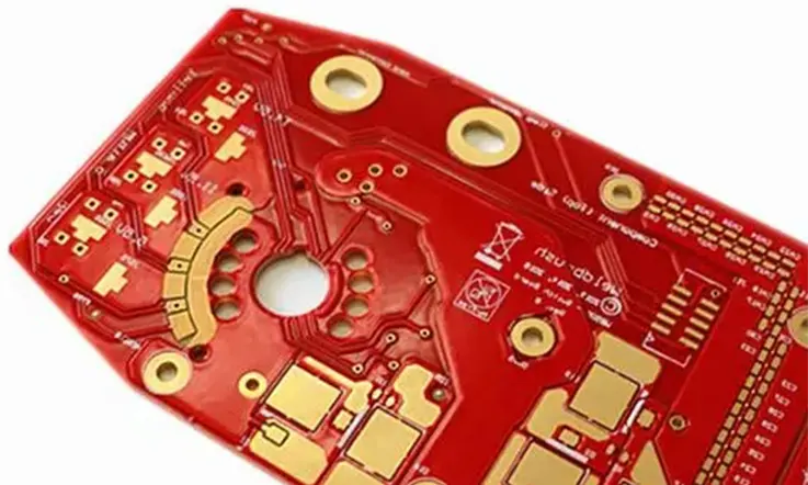
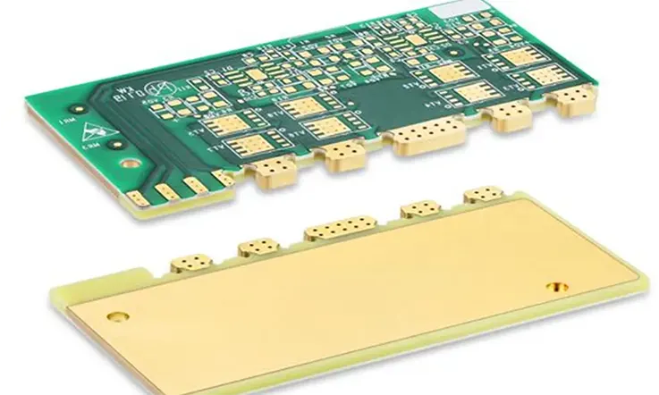
Introduction to Heavy Copper PCBs
Heavy copper PCBs, an enhanced version of Printed Circuit Boards, are meticulously designed to include significantly thicker copper layers or traces, usually surpassing the standard copper thickness of 1oz/ft². They excel in managing substantial current capacities and provide increased reliability and durability, especially in adverse environmental conditions.
The copper weight, a defining feature of these PCBs, is determined by the thickness and dimensions of the copper layers incorporated. Distinguished by their heightened copper weight, typically quantified in ounces (oz) or grams (g) per square foot or square meter, heavy copper PCBs are notable for their ability to conduct higher currents and their superior thermal regulation proficiencies.
Standard PCBs generally incorporate copper weights of 1 oz (28.35 g) or 2 oz (56.70 g) per square foot. Nevertheless, heavy copper PCBs diverge from this norm, providing copper weights that commence from 3 oz (85.05 g) and possibly reaching up to 20 oz (567 g) or beyond per square foot.
The decision to augment the copper weight in these PCBs promotes efficient conduction of higher currents and improves thermal performance. However, the specific weight of a given heavy copper PCB is influenced by multiple factors, including its overall dimensions, copper thickness, and other unique design attributes.
Heavy copper PCBs find their extensive application in domains demanding high power accommodation and exceptional thermal regulation, including power electronics, aerospace, military, and industrial instances. The elevated copper weight considerably amplifies the PCB’s competence to withstand high temperatures and promotes efficient heat dispersion. This positions these boards as a suitable choice for applications with rigorous thermal necessities. The manufacturing of heavy copper PCBs entails a range of procedures, including plating, etching, and lamination, which are adaptable to meet specific design preferences.
Testing and Inspection of Heavy Copper PCBs
As a part of ensuring the performance and reliability of heavy copper PCBs, stringent testing and inspection procedures become highly consequential. The incorporation of these methodologies entails various techniques:
Visual Analysis: Acting as the preliminary stage of quality control, visual inspections carefully examine the PCB for external irregularities such as abrasions, fractures, and indications of delamination.
X-ray Evaluation: Adopting a non-invasive method, x-ray inspections enable an in-depth investigation of PCBs, locating concealed defects like voids, cracks, and internal delamination. This analysis is pivotal in appraising the solder joint’s solidity and the status of internal vias.
Cross-Section Examination: This procedure requires the extraction of a minuscule section of the PCB for thorough microscopic scrutiny. It aids in gauging the thickness of the copper layer, the quality of plating, and detection of internal inconsistencies.
Electrical Assessment: By estimating the electrical characteristics of the PCB, including resistance, capacitance, and impedance, electrical assessments help in detecting electrical anomalies like shorts or opens.
Thermal Evaluation: To assess the thermal durability, these tests subject the PCB to high temperature conditions. This helps to identify thermally-induced distortions such as delamination or crack development.
Environmental Assessment: This procedure subjects the PCB to various environmental stress conditions, including shifts in temperature, humidity, and vibration. The aim is to determine its resilience and stability under different conditions.
Solderability Examination: This testing is aimed at evaluating the PCB’s ability to form an effective bond with solder. It assists in identifying possible issues related to the surface finish or plating.
Heavy Copper Circuit Boards: Advantages and Uses
The primary merit of heavy copper circuit boards resides in their extraordinary resilience to damaging repercussions linked with elevated current flows, high temperatures, and the rigors of thermal cycling. This contrasts significantly with traditional circuit boards that, under such strenuous circumstances, may falter in a brief timespan, while heavy copper boards exhibit unmatched fortitude. This remarkable robustness renders heavy copper boards supremely apt for deployment in rigorous contexts, notably in sectors like defense and aerospace. Furthermore, these boards are discerned by their exceptional tolerance capacities, ensuring consistent, high-level performance even under testing operational situations. Beyond their hardiness, heavy copper circuit boards extend a host of additional benefits, enhancing their versatility and applicability across an extensive range of applications.
Advantages of Heavy Copper Circuit Boards
Enhanced Power Handling Capabilities: The incorporation of thicker copper layers in heavy copper circuit boards facilitates the management of substantially higher current loads. This attribute renders them particularly advantageous for deploying in scenarios demanding the integration of high-power components or systems.
Superior Thermal Management: Owing to their increased copper mass, heavy copper circuit boards exhibit superior heat dissipation characteristics. The augmented copper surface area plays a pivotal role in more effectively dispersing heat emanating from power components, thereby mitigating overheating risks and enhancing overall thermal regulation.
Augmented Durability and Reliability: Heavy copper circuit boards are synonymous with enhanced mechanical robustness and longevity. The presence of thicker copper layers contributes to improved structural stability, equipping the boards to withstand temperature fluctuations, mechanical stresses, and vibrational forces more adeptly.
Minimized Voltage Drop: The diminished electrical resistance associated with the heavier copper layers leads to a reduction in voltage drop along the traces. This characteristic ensures optimal power distribution, facilitating the more efficient operation of applications necessitating high currents.
Increased Design Versatility: Heavy copper circuit boards afford designers a greater latitude in power routing and trace dimensioning. The feasibility of utilizing wider traces coupled with the substantial copper mass enables the conception of more resilient and efficacious designs, particularly pertinent to high-power applications.
Uses of Heavy Copper Circuit Boards
Within power electronics domains, heavy copper circuit boards serve as cornerstones for uses such as power converters, motor drives, inverters, as well as uninterruptible power supply (UPS) frameworks. These use cases, marked by high-power components, call for superior thermal regulation capabilities.
In the automotive and transit sectors, heavy copper circuit boards are crucial for diverse uses encompassing electric vehicle (EV) powertrains, battery management systems, automotive lighting arrangements, and EV charging infrastructure. Owing to their adeptness at handling heavy current loads and their superior heat mitigation traits, they prove ideal for meeting the stringent demands inherent to automotive contexts.
In renewable energy segments, heavy copper circuit boards contribute significantly to solar inverters, wind energy arrangements, and energy storing solutions. Their incorporation in these configurations facilitates the management of increased current demands, effectively enhancing the dependability and thermal efficacy of renewable energy structures.
Within industrial machinery and equipment requiring high-power output and reliable functioning, heavy copper circuit boards are the favored technology. They find comprehensive deployment in robotics, automation assemblies, motor control units, and industrial control boards, among other things.
On the aerospace and defense front, where high-power output and robust reliability are paramount, heavy copper circuit boards are vastly deployed. Usage ranges from avionics structures, radar apparatus, satellite technology, to communication systems, highlighting the vital part heavy copper circuit boards play in bolstering advanced technological applications across a myriad of industries.
Difference Between Copper PCB and Heavy Copper PCB?
Notwithstanding their lexical similarities, Copper PCB and Heavy Copper PCB are distinctly diverse constructs with considerable differences in their traits and deployments.
Copper PCBs are characterized by employing a copper-founded substrate, significantly enhancing thermal dissipation competencies thereby extending the operational longevity of the PCB’s constituents. The copper substrate serves as an adept heat transfer medium, channelling heat from the PCB’s inner components towards external cooling fixtures such as heat sinks or metallic casings. Copper’s superior thermal conductivity, exceeding that of other metals to reach up to 401 W/m.K, accounts for this proficiency.
In contrast, a Heavy Copper PCB, also designated as a Thick Copper PCB, is distinguishable by incorporating a copper layer where the thickness surpasses 3OZ. This variant avails multiple substrate materials like copper, aluminum, or FR4. An outstanding attribute of Heavy Copper PCBs resides in their capability to conduct voluminous current levels, making them inherently appropriate for deployments necessitating significant power supply. Fundamentally, it is essential to discern that within this sphere, “thick copper” distinctly refers to the copper foil’s thickness fused onto the PCB, as opposed to the cumulative thickness of the PCB in itself. This thickening process of the copper foil pertains to PCBs constituted from both aluminum and FR4 materials.
Send a RFQ for Your Custom Thick Copper PCB
Should you require additional information on heavy copper PCBs or wish to enquire about the latest pricing, we encourage you to reach out to us. Leveraging our specialized knowledge in heavy copper PCB technology, we are equipped to offer nuanced advice that aligns with your specific requirements. You are welcome to upload your Gerber file via our quick quote portal for an expedient assessment. The dedicated customer service team at JarnisTech is prepared to efficiently handle your questions, furnish you with professional guidance, and extend competitive pricing solutions.
Related Posts:
- Heavy Copper PCB
- 2 Oz Copper PCB: Design, Manufacturing Application And Benefits
- Why 30Z Copper PCB Often Used in Electronic Equipment
- 4 Oz Copper PCB Manufacturing and Assembly Supplier
- Comprehensive FAQ Guide About 60Z Copper PCB Board
- Comprehensive Overvierofthe Capabilities of 10 oz Copper PCB
- 20 Oz Copper PCB Supplier and Manufacturer in China