
The need for reliable and efficient thermal management in modern electronics has never been higher. As industrial applications grow more demanding, the materials and solutions we use to power these systems must keep pace. Enter Copper Base PCBs (Printed Circuit Boards), a powerful alternative to traditional PCBs. With their exceptional thermal conductivity and durability, Copper Base PCBs are shaping the future of industries that require high power and performance, from automotive to renewable energy.
In this article, we’ll explore the technology behind Copper Base PCBs, examine how they outperform traditional alternatives, and delve into their real-world applications across various sectors. Whether you’re an engineer, manufacturer, or someone exploring new PCB solutions, this guide will shed light on the critical aspects of Copper Base PCBs and how they can meet the needs of high-power systems.
Why Copper Base PCBs Are Transforming Industrial?
The demand for high-performance electronics across industries is skyrocketing, and as systems evolve, so does the need for efficient thermal management. Copper Base PCBs are at the forefront of this transformation, offering a robust solution to the heat challenges faced by high-power and high-performance devices. From automotive applications to LED lighting and renewable energy systems, Copper Base PCBs are paving the way for next-generation electronics.
The rise of high-performance electronics is tied directly to increasing energy efficiency, faster processing speeds, and greater power densities in compact systems. As a result, This shift has intensified the focus on managing heat effectively in modern circuit designs. With its outstanding thermal conductivity, copper serves as a highly effective and durable material to address the demands of heat-intensive electronic applications.
How Copper Base PCBs Revolutionize Thermal Management?
When it comes to effective heat management, Copper Base PCBs stand out from the crowd. The fundamental reason is simple: copper is one of the most thermally conductive metals available, which means it dissipates heat more efficiently than other materials used in traditional PCBs. In high-power applications, where heat is generated continuously, these PCBs offer efficient heat dissipation, helping to maintain system stability and extend the lifespan of the components.
Why Copper-
Copper’s superior heat dissipation capabilities make it ideal for high-power systems that demand fast and efficient thermal management. In comparison to alternatives like aluminum, copper outperforms when it comes to spreading heat quickly and evenly across the board. This property is especially beneficial in systems like power electronics, where temperature regulation can make or break the performance of the equipment.
Copper does more than just handle heat—it enhances electrical performance too. Thanks to its low resistance, it minimizes power loss in high-current circuits. This helps energy flow more efficiently, ensuring that less power is wasted. With copper, circuits run smoother, and energy transfer is more effective, especially in systems where reliability is a must.
The Rise of High-Performance Electronics
In the last few years, industrial sectors like automotive, renewable energy, and advanced electronics have seen a significant shift toward more efficient, high-performance systems. As electronic devices consume more power and function in increasingly compact designs, heat management becomes one of the biggest challenges. Without effective solutions, excessive heat can cause performance degradation and even failure of sensitive components.
Growing Demand for Efficient Thermal Management Solutions-
High-power electronics require solutions that go beyond simple insulation and need to focus on how to efficiently dissipate heat without sacrificing performance. Copper Base PCBs have emerged as a top contender in this space due to their unmatched ability to transfer heat, improving reliability and efficiency. The increasing complexity of modern electronics—such as electric vehicles (EVs), LED lighting, and industrial automation—only amplifies the importance of using advanced thermal management solutions.
| Electronics Application | Thermal Management Challenge | Solution |
| Electric Vehicles (EVs) | High power components generate significant heat. | Copper Base PCBs provide superior heat dissipation. |
| LED Lighting | High-output LEDs produce excess heat. | Copper Base PCBs ensure efficient thermal management. |
| Industrial Automation | Power control systems under heavy load. | Copper Base PCBs prevent overheating, enhancing system longevity. |
With the growing trend toward energy-efficient solutions and the increasing power requirements of industrial equipment, Copper Base PCBs are meeting the need for superior heat dissipation.
Meeting Industry Needs Through Innovation
Industries are in constant search of ways to improve the efficiency and durability of their products. Copper Base PCBs meet these demands through continuous innovation, offering tailored solutions for various sectors. The adoption of Copper Base PCBs has surged in applications like automotive, renewable energy, and LED lighting due to their effectiveness in handling high current loads and ensuring reliability.
Applications in Automotive, LED Lighting, and Renewable Energy Systems:
1.Automotive Industry-
Electric vehicles are becoming more common, and with them, the demand for high-performance, energy-efficient systems. Copper Base PCBs are a key component in automotive applications, particularly in the power electronics used for motors, inverters, and battery management systems (BMS). These components require efficient thermal management to maintain high performance over long periods. Copper Base PCBs meet this need by offering excellent heat dissipation, preventing components from overheating and ensuring long-term reliability in harsh conditions.
| Automotive Application | Copper Base PCB Role | Benefits |
| Inverters | Distribute heat from power electronics. | Improve efficiency and reliability. |
| Battery Management Systems | Prevent heat buildup in charging units. | Increase system lifespan. |
| Motors | Efficient heat transfer from motor circuits. | Maintain optimal performance. |
2.LED Lighting-
High-power LED systems, especially in commercial and industrial settings, are vulnerable to heat. When LEDs overheat, they can lose luminosity, degrade faster, and fail prematurely. Copper Base PCBs prevent these issues by effectively transferring heat away from the LED components, ensuring they operate within safe temperature ranges. This leads to longer-lasting, more efficient lighting solutions.
| LED Lighting System | Thermal Solution | Outcome |
| High-output LEDs | Use of Copper Base PCBs for heat dissipation. | Reduced risk of thermal failure. |
| LED Drivers and Controllers | Copper Base PCBs manage heat from electronics. | Extended lifespan and reduced maintenance costs. |
In the realm of LED lighting you’ll come across four varieties of copper circuit boards:
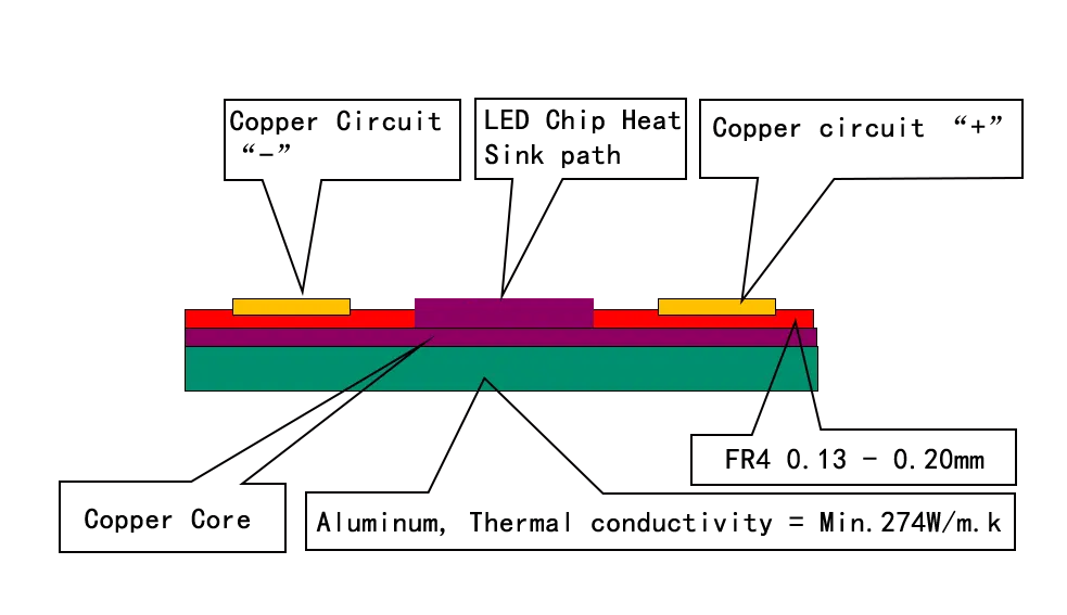
● The direct thermal pathway without a dielectric layer is an aluminum-copper PCB. This type of PCB is designed to provide a direct thermal pathway without an insulating dielectric layer between the aluminum base and copper traces, enabling quicker dissipation of heat. The aluminum substrate provides excellent thermal conductivity properties, while the copper traces enable efficient electrical current carry capacity. Consequently, these PCBs are ideal for high power LED lighting and other applications requiring efficient heat dissipation and high power handling capabilities. Our PCB manufacturing facility produces these aluminum-copper PCBs to meet the specific requirements and demands of our clients.
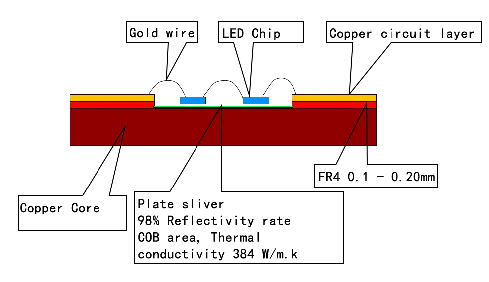
● The COB Copper PCB (Chip on Board Copper PCB) is designed to provide a direct thermal connection between the LED chip and the copper substrate. In this setup, the LED chip is mounted directly onto the copper layer, allowing heat to transfer efficiently and dissipate quickly. This design works best for high-power LED applications where managing heat is a major concern. By ensuring optimal heat dissipation, this configuration enhances the performance and longevity of the system, making it a solid choice for demanding, heat-sensitive applications.
At our PCB manufacturing facility, we specialize in producing customized COB Copper PCBs tailored to meet the unique needs of our clients. These Copper PCBs are perfect for high-power LED applications, where managing heat effectively is a top priority. By ensuring that thermal dissipation is handled with precision, our COB Copper PCBs help boost performance and extend the lifespan of your systems. Whether you’re looking to meet specific power and thermal requirements or seeking a reliable solution for demanding applications, we’ve got you covered. Reach out today and let us help you take your design to the next level!
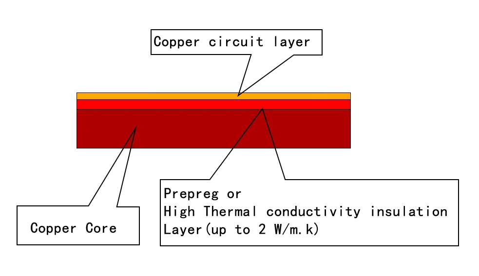
● The standard stack-up for Copper PCBs with a core utilizes a traditional construction, which includes copper trace layers and insulating dielectric layers. A copper core is added to this setup to boost thermal conductivity, reaching up to 12 W/m.k. This structure is well-suited for applications that require effective heat management, ensuring consistent performance over time. With this design, systems can handle high power loads without overheating, providing a reliable and efficient solution for demanding electronic applications.
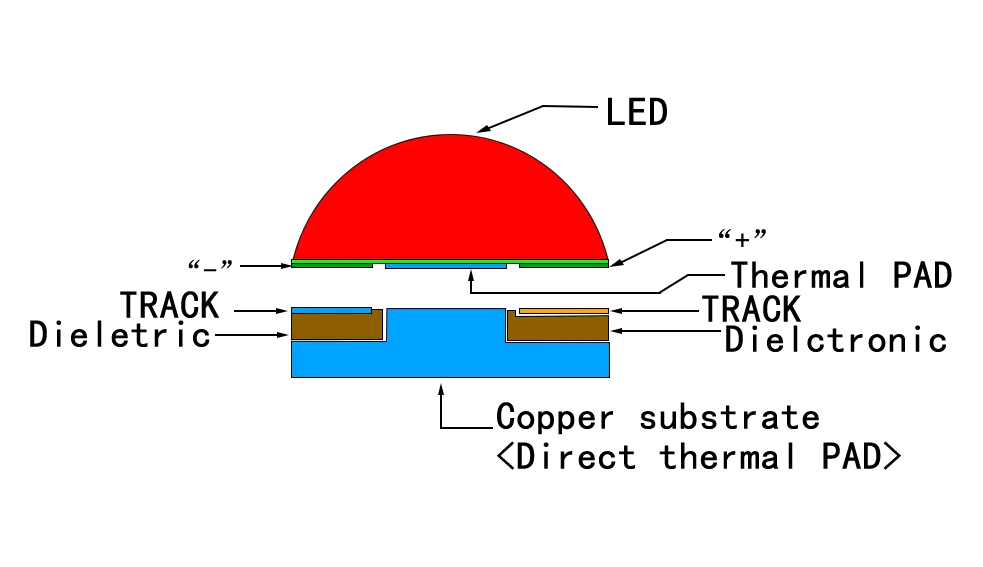
● The proposed setup ensures direct thermal conduction by eliminating any dielectric layer beneath the thermal pad. This design offers an uninterrupted heat transfer path, allowing for more efficient dissipation of heat. By removing extra layers, the system minimizes resistance to heat flow, making it well-suited for applications where temperature management is a top priority. With this approach, thermal performance is enhanced, giving the device a better chance to handle higher power levels without overheating.
3.Renewable Energy Systems-
The renewable energy sector relies heavily on inverters and power controllers to convert energy from solar panels and wind turbines into usable electricity. These systems tend to operate under heavy load conditions, generating substantial heat. Copper Base PCBs ensure that these systems maintain peak efficiency by dissipating heat effectively, thereby enhancing the performance and longevity of renewable energy systems.
| Renewable Energy Application | Copper Base PCB Benefit | Impact |
| Solar Inverters | Superior heat dissipation during operation. | Reliable performance over time. |
| Wind Turbine Controllers | Effective heat transfer from power modules. | Prevent component failure due to heat. |
Structural and Material Components of Copper Base PCBs
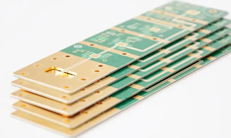
Copper Base PCBs are a powerhouse in electronic design, primarily due to their unique structural and material components. These boards are engineered with precision to handle high-current and high-thermal demands, making them indispensable for industries like automotive electronics, LED lighting, and power systems. Let’s dive into the essential components that make these PCBs a preferred choice for demanding applications.
Layers and Composition of Copper Base PCBs
At the heart of every Copper Base PCB lies a meticulous arrangement of layers and materials. These boards typically comprise three primary layers: the copper core, insulation material, and surface coatings. Each layer is carefully selected to optimize performance under high-stress conditions.
1.Copper Core-
The copper core serves as the primary thermal and electrical conductor. It is available in various thicknesses, tailored to the power and thermal requirements of the application. Thicker cores are often used in high-power systems, ensuring efficient heat transfer and reduced thermal resistance.
2.Insulation Material-
This layer provides electrical isolation between the copper core and the circuits. High-quality materials like polyimide or ceramic-filled polymers are commonly used for their excellent thermal conductivity and dielectric strength.
3.Surface Coatings-
The surface is typically treated with coatings such as solder mask, silkscreen, or anti-oxidation layers to protect the circuits from environmental damage and ensure solderability.
Layer Comparison for Copper Base PCBs-
| Layer | Material Options | Function | Advantages |
| Copper Core | Pure copper, copper alloy | Heat dissipation, electrical conduction | High conductivity, durability |
| Insulation Layer | Ceramic, polyimide | Electrical isolation, thermal transfer | High heat resistance, reliability |
| Surface Coating | Solder mask, anti-oxidation | Protection, solderability | Enhanced longevity, easy assembly |
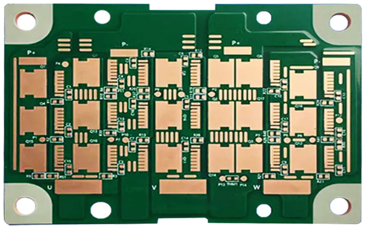
Multi-Layer Copper Base PCBs for Advanced Applications
For applications that demand compact designs and increased functionality, multi-layer Copper Base PCBs are the go-to solution. These boards consist of multiple layers of copper cores and circuits, separated by insulating materials, and they are designed to handle complex electronic systems.
Advantages of Multi-Layer Designs-
●Enhanced Power Distribution: Multiple copper layers allow efficient distribution of electrical power across the board. This is particularly beneficial for high-current applications, such as industrial automation systems.
●Improved Heat Dissipation: Stacked copper cores and thermal vias ensure that heat is distributed evenly, reducing the risk of hotspots and improving the lifespan of components.
●Compact Design: Multi-layer PCBs enable the integration of more circuits within a smaller footprint, making them ideal for compact devices like LED modules and wearable technology.
Example Use Case:
In LED lighting systems, multi-layer Copper Base PCBs are used to manage the high heat generated by LEDs. The boards’ thermal conductivity ensures uniform temperature across the system, reducing thermal stress and enhancing brightness consistency.
The Importance of Material Selection in PCB Design
Choosing the right materials can make all the difference in PCB manufacturing. A subpar material selection can lead to major headaches down the road, while high-quality materials ensure that everything runs smoothly, lasts longer, and performs better. When done right, the choice of materials can be the key to keeping production costs down and efficiency up. It’s one of those details that you don’t really notice—until something goes wrong. Get it right, and it’s like having the right tools in the toolbox—they just work.
Factors to Consider When Choosing Materials-
●Thermal Conductivity: For high-power systems, materials with excellent thermal transfer properties, such as copper and ceramic-based insulators, are preferred.
●Electrical Performance: High-frequency applications benefit from materials with low dielectric losses, ensuring signal integrity.
●Durability and Reliability: Industrial and automotive systems require materials that can withstand harsh environments, including extreme temperatures, vibrations, and moisture.
Material Selection Table-
| Material | Ideal Applications | Benefits |
| Copper Core | High-power devices, automotive | Superior heat transfer, conductivity |
| Ceramic Insulator | LED lighting, renewable energy | High thermal stability, electrical isolation |
| Polyimide Substrate | Flexible PCBs, wearable electronics | Flexibility, thermal resistance |
Case Study:
In renewable energy systems like wind turbines, Copper Base PCBs with ceramic insulators are used to manage power electronics. These materials provide excellent thermal conductivity and ensure reliable performance in fluctuating environmental conditions.
Copper Base PCB Design Considerations
Designing a Copper Base PCB requires a well-thought-out mix of technical skills and careful planning. From handling heat dissipation to refining signal routing, each aspect contributes to making the board function reliably in challenging conditions. Let’s look at the factors that can help you craft Copper Base PCBs that perform at their best.
1.Thermal Management: Keeping It Cool Under Pressure
Copper Base PCBs are often the go-to choice for high-power applications because of their outstanding heat dissipation capabilities. Managing thermal performance involves more than just leveraging copper’s high conductivity; it’s about strategically designing the board to handle heat distribution effectively.
●Thermal Vias: Add thermal vias in high-heat zones to channel heat away from critical components.
●Heat Sinks Integration: Utilize heat sinks in combination with the copper core for enhanced cooling.
Real-Life Example: Consider an LED floodlight where excessive heat can degrade performance. Copper Base PCBs with embedded heat sinks maintain consistent brightness and prolong the system’s life.
Pro Tip: Want your PCBs to handle the heat like a champ? Focus on thermal modeling during the design phase.
2.Meeting Electrical and Mechanical Demands
Each application presents its own unique set of electrical and mechanical demands. Achieving the necessary performance involves more than just meeting basic specifications—it requires precise design and thorough engineering to ensure the PCB operates reliably under all expected conditions.
●Voltage and Current Capacity: Choose copper thickness based on your power requirements. For example, a 2 oz copper layer can handle currents up to 30A with minimal resistance.
●Dimensions and Tolerances: Ensure the PCB layout adheres to strict mechanical tolerances, especially for automotive and industrial equipment.
Copper Thickness and Current Capacity-
| Copper Thickness (oz/ft²) | Current Capacity (A) | Recommended Applications |
| 1 | Up to 20 | General electronics |
| 2 | 20–30 | High-power LED systems |
| 3 | 30+ | Heavy-duty industrial controllers |
3.Thoughtful Material Selection
The choice of materials for a Copper Base PCB directly affects its durability and performance. Selecting the right insulating layer, copper core, and surface finish is paramount for optimal results.
●Insulating Materials: Use polyimide or ceramic for applications requiring excellent thermal resistance.
●Copper Core: High-purity copper ensures consistent conductivity and minimal resistance.
●Surface Finish: Choose between HASL, ENIG, or OSP finishes depending on the environmental conditions and solderability requirements.
Example: A renewable energy inverter subjected to harsh outdoor conditions would benefit from a polyimide insulator and an ENIG finish for corrosion resistance.
4.Component Placement: Setting the Stage for Performance
Placing components on a Copper Base PCB is like arranging actors in a play—every role needs to shine without overshadowing others.
●High-Power Components: Position these near the edges to allow heat to dissipate freely.
●Signal and Power Separation: Avoid interference by keeping signal traces away from high-current paths.
An industrial motor controller PCB shows high-power MOSFETs placed on the periphery, with signal components centrally located, reducing cross-talk and improving overall efficiency.
5.Ground Plane Design: Stability and Performance
A solid ground plane isn’t just about heat dissipation—it also minimizes electrical noise and provides mechanical strength.
●Thermal Benefits: A thicker ground plane enhances heat dissipation.
●EMI Shielding: A continuous ground plane helps reduce electromagnetic interference, ensuring sensitive signal paths remain unaffected.
Fun Fact: Some automotive designs use multiple ground planes to optimize signal integrity in complex systems.
6.Signal Routing: Clear Paths for Clear Signals
Efficient signal routing helps reduce noise and maintain signal integrity, especially in multi-layer Copper Base PCBs. By carefully managing the trace paths and layout, we can minimize electromagnetic interference, ensuring the circuit performs as expected in demanding environments. This strategic routing approach prevents signal degradation and cross-talk, safeguarding the quality of the overall system
●Avoid Overlaps: Ensure power and signal traces do not overlap to minimize interference.
●Electromagnetic Field Mitigation: Use shielded vias and ground plane connections to combat EMI.
Common Routing Challenges and Solutions-
| Challenge | Solution |
| Signal Overlap | Increase spacing between traces |
| High EMI | Use grounded shielding and copper pours |
| Loss of Signal Quality | Shorten trace lengths and minimize bends |
7.Manufacturing Feasibility: Designing for Production
Even the most innovative design is of little use if it can’t be manufactured. Collaborating with your PCB manufacturer early in the process ensures your design aligns with production capabilities.
●Copper Plating: If your design needs thicker copper layers, verify the plating capacity with the manufacturer.
●Etching Precision: Intricate designs may require advanced etching technology.
Pro Tip: Keep the communication lines open with your manufacturer to avoid hiccups during production.
Customization and Manufacturing of Copper Base PCBs
The manufacturing and customization of Copper Base PCBs is a detailed process that marries precision engineering with industry-specific requirements. From automotive to industrial lighting systems, these PCBs are meticulously crafted to deliver optimal performance. Below, we explore the intricacies of customization, advanced manufacturing techniques, and rigorous quality assurance measures.
Advanced Customization for Industry-Specific Needs
Copper Base PCB production isn’t a one-size-fits-all solution. Different sectors, like automotive electronics, industrial automation, and LED lighting, require custom designs to meet their specific performance standards. For example, automotive electronics need durability and heat resistance, while LED lighting solutions focus on managing thermal performance to avoid overheating. By tailoring the design for each industry’s particular needs, we can ensure the PCB delivers consistent and reliable results, maximizing efficiency and meeting the unique challenges of each application. This approach guarantees the product performs at its best when it’s needed most.
1.Automotive Electronics: Automotive systems require PCBs that can endure high temperatures and vibrations. Custom copper thickness and insulation materials are often employed to meet these demands.
2.Industrial Automation: Heavy machinery and industrial equipment rely on Copper Base PCBs with enhanced thermal management. Custom multi-layer designs are frequently used to integrate complex control circuits within a compact space.
3.LED Lighting Systems: Lighting manufacturers prioritize PCBs that can effectively manage heat to avoid any drop in brightness over time. For this, custom copper layouts combined with thermal vias are a must, as they help ensure heat is efficiently transferred away from the light source. This design approach ensures that illumination remains steady and consistent, preventing any degradation in performance.
Customization Table: Industry Needs and PCB Solutions-
| Industry | Customization Feature | Purpose | Benefit |
| Automotive | High copper thickness, vibration-proof | Withstand harsh conditions | Enhanced durability and reliability |
| Industrial Equipment | Multi-layer designs, thermal vias | Efficient heat management | Improved operational efficiency |
| LED Lighting | Precise copper layouts, ceramic insulators | Maintain brightness and lifespan | Consistent lighting performance |
Precision in Manufacturing Processes
The production of Copper Base PCBs is a meticulous journey that relies on cutting-edge technology and skilled craftsmanship. Advanced manufacturing processes ensure these boards deliver the precision and performance demanded by modern industries.
Key Manufacturing Techniques-
●Copper Etching: This process defines the circuit paths by removing unnecessary copper from the board. Precision in etching is necessary to create complex designs, especially in tight spaces and multi-layer structures. The accuracy achieved during this step directly affects the performance of the final product, ensuring that the traces are perfectly positioned to deliver reliable functionality. In applications where size is limited and design complexity is high, precise etching makes all the difference, enabling the circuit to function optimally without interference or errors.
●Multi-Layer Lamination: Multi-layer PCBs are created by stacking and bonding several layers of copper and insulation materials under high pressure and temperature. This technique is widely used for complex designs in automotive and industrial systems.
●Laser Drilling: To connect layers in multi-layer PCBs, laser drilling is employed to create microvias. This method ensures minimal thermal stress and maintains the integrity of the board.
Imagine an industrial-grade motor controller. The PCB’s copper paths are etched to handle high currents without overheating, while laser-drilled vias ensure seamless inter-layer connections. This precision engineering guarantees optimal performance in demanding environments.
Quality Assurance in High-Performance PCB Production
Ensuring the reliability of Copper Base PCBs involves stringent quality assurance measures at every production stage. From material selection to final testing, each step is designed to uphold the highest standards of durability and performance.
Quality Assurance Steps-
●Material Inspection: All raw materials, including copper sheets and insulators, are rigorously inspected for consistency and quality.
●Electrical Testing: Each PCB undergoes comprehensive electrical tests to verify circuit integrity, resistance levels, and current-carrying capacity.
●Thermal Testing: Heat resistance and dissipation capabilities are tested under simulated operating conditions to ensure the board performs as expected.
Consider a renewable energy inverter. During production, its Copper Base PCB undergoes thermal testing at elevated temperatures to simulate real-world operating conditions. This ensures the board will perform reliably in solar power systems exposed to extreme heat.
QA Process Overview Table-
| Step | Purpose | Testing Methods |
| Material Inspection | Verify consistency and quality | Visual inspection, material analysis |
| Electrical Testing | Ensure circuit integrity | Continuity testing, impedance checks |
| Thermal Testing | Assess heat dissipation capabilities | Thermal imaging, load testing |
Comparing Copper Base PCBs with Aluminum Core Alternatives
Choosing the ideal core material for printed circuit boards (PCBs) is a decision rooted in technical performance, application-specific requirements, and cost-effectiveness. Copper and aluminum are the two most prevalent core materials, each offering distinct benefits. Let’s dive deeper into the engineering considerations, technical metrics, and real-world applications that shape this critical choice.
Thermal Conductivity and Efficiency: The Heat Equation
Heat dissipation is often the driving factor in selecting the core material for PCBs used in high-power and high-heat environments. Copper and aluminum differ significantly in their thermal performance, which directly impacts the efficiency and lifespan of the PCB and its components.
1.Intrinsic Thermal Conductivity-
Copper’s thermal conductivity is 398 W/mK, nearly double that of aluminum, which averages around 205 W/mK. This property allows Copper Base PCBs to conduct heat away from critical areas faster, ensuring stable operation under extreme conditions.
2.Thermal Resistance in Real-World Applications-
While raw thermal conductivity is an essential metric, the effectiveness of a PCB in dissipating heat also depends on factors like layer design, thickness, and surface area. Copper Base PCBs allow for thinner layers with lower thermal resistance, enhancing their heat transfer capabilities.
Thermal Conductivity Comparison-
| Parameter | Copper Base PCBs | Aluminum Core PCBs |
| Thermal Conductivity (W/mK) | 398 | 205 |
| Heat Dissipation Efficiency | Excellent | Moderate |
| Optimal Application | High-power systems | General-purpose systems |
Example: In high-intensity LED floodlights, Copper Base PCBs help maintain uniform light output by reducing thermal strain on individual diodes, leading to better energy efficiency and longevity.
Advanced Thermal Management Techniques
●Integrated Heat Sinks: Copper Base PCBs can incorporate integrated heat sinks directly into the design, minimizing the need for external thermal management solutions. These heat sinks can be strategically placed in high-power areas, improving overall system performance.
●Hybrid Layer Designs: Advanced designs use a hybrid of copper and aluminum to balance cost and performance. Copper layers are placed in regions requiring exceptional thermal conductivity, while aluminum is used in less critical zones.
●Simulation and Modeling: Our PCB engineers often use thermal simulation tools to analyze heat distribution in Copper Base PCBs, ensuring the design meets application-specific thermal demands without overengineering.
Cost Considerations for Industrial Applications
The financial aspect cannot be overlooked, especially in large-scale production or cost-sensitive industries. Copper offers unparalleled performance, but its cost can be prohibitive in some cases.
1.Material Pricing Dynamics-
Copper prices fluctuate more significantly in global markets compared to aluminum. For applications requiring a balance of thermal management and affordability, aluminum core PCBs may offer a viable alternative.
2.Total Lifecycle Cost-
While copper has a higher upfront cost, its superior durability and reliability can lead to reduced maintenance and replacement expenses over the product’s lifecycle.
Material Cost Comparison-
| Cost Aspect | Copper Base PCBs | Aluminum Core PCBs |
| Initial Material Cost | Higher | Lower |
| Manufacturing Complexity | Higher | Moderate |
| Long-Term Durability | Superior | Moderate |
Case Study: A leading manufacturer of renewable energy inverters evaluated lifecycle costs and found that while Copper Base PCBs had a 30% higher initial expense, their extended operational lifespan reduced overall costs by 20% over five years.
Use Cases: When Copper Triumphs
Certain industries and applications demand the unmatched properties of Copper Base PCBs. Let’s examine the sectors where copper outshines aluminum and explore why these scenarios benefit from its superior characteristics.
1.Automotive and Electric Vehicles (EVs)-
In EV battery management systems, Copper Base PCBs ensure consistent thermal regulation across cells, improving battery efficiency and extending its lifespan. Aluminum cores, while lighter, fail to meet the thermal demands of these systems under high loads.
2.High-Power LED Systems-
Applications such as stadium lighting, architectural installations, and UV curing systems rely on Copper Base PCBs to handle the heat generated by high-wattage LEDs, preventing lumen depreciation over time.
3.Industrial Control Systems-
In motor controllers and high-current power supplies, the ability of Copper Base PCBs to handle substantial electrical loads while dissipating heat efficiently minimizes failure rates, even in demanding industrial environments.
Comprehensive Comparison of Copper Base PCBs with FR4, Flexible, and Ceramic PCBs
To make an informed choice among Copper Base PCBs, FR4, Flexible, and Ceramic PCBs, we must delve into the nuances of materials, manufacturing complexity, cost implications, performance parameters, and application scenarios. Below, we break down these aspects, enabling a deeper understanding of their unique strengths and trade-offs.
1.Material Composition: Strengths and Limitations
●Copper Base PCBs:Utilize a copper substrate for unmatched thermal conductivity and mechanical robustness. This composition is ideal for dissipating heat in high-power applications like LED modules and automotive systems.
●FR4: Composed of glass-reinforced epoxy laminate, FR4 is cost-effective but limited in thermal management, making it suitable for low-power applications.
●Flexible PCBs: Employ polyimide films or other flexible materials that allow bending and folding. While they excel in compact and dynamic applications, their heat dissipation and mechanical strength are comparatively lower.
●Ceramic PCBs: Use ceramic materials like alumina (Al2O3) or aluminum nitride (AlN) for good thermal performance and electrical insulation. They are brittle but perform well in high-frequency or thermal-stable environments.
2.Manufacturing Complexity
| PCB Type | Manufacturing Complexity | Key Processes |
| Copper Base PCBs | High | Advanced copper etching, multi-layer lamination |
| FR4 | Low | Standard PCB manufacturing, suitable for mass production |
| Flexible PCBs | Medium | Requires specialized processes for flexible substrates |
| Ceramic PCBs | Medium-High | Involves sintering and precise deposition of circuits |
●Copper Base PCBs: The process includes copper etching, which requires precision to maintain conductivity and durability.
●Flexible PCBs: Manufacturing challenges include achieving consistent signal integrity across bendable layers.
●Ceramic PCBs: Require sintering processes that increase cost and complexity but ensure excellent performance in niche applications.
3.Cost Analysis: Balancing Investment and Return
Copper Base PCBs are at the higher end of the cost spectrum due to the price of copper and the intricate manufacturing steps involved. However, their reliability in high-stress environments justifies the investment.
| PCB Type | Relative Cost | Cost Drivers |
| Copper Base PCBs | High | Copper material cost, advanced manufacturing |
| FR4 | Low | Economical materials and simple processes |
| Flexible PCBs | Medium | Specialized materials like polyimide |
| Ceramic PCBs | Medium-High | Expensive raw materials and sintering process |
4.Performance Parameters: How They Measure Up
| Parameter | Copper Base PCBs | FR4 | Flexible PCBs | Ceramic PCBs |
| Thermal Conductivity | 398 W/mK | 0.3 W/mK | 0.1 W/mK | 20–200 W/mK |
| Dielectric Strength | High | Medium | Medium | Very High |
| Mechanical Strength | Very High | High | Low | High |
| Flexibility | None | None | High | None |
●Copper Base PCBs: Leading in thermal conductivity and mechanical durability, making them indispensable for high-power circuits.
●FR4: Adequate for general-purpose electronics but falters under high heat or stress.
●Flexible PCBs: Excellent for dynamic systems requiring bending but with reduced mechanical strength.
●Ceramic PCBs: Offer a balance of thermal and electrical performance but are fragile and costlier.
5.Application Scenarios: Finding the Right Fit
Copper Base PCBs-
●High-power LEDs: Dissipate heat effectively, ensuring longevity.
●Automotive Electronics: Handle vibration and extreme temperatures.
●Renewable Energy Systems: Enhance thermal stability in solar inverters and wind turbines.
FR4-
●Commonly found in consumer electronics like computers and TVs due to affordability and versatility.
Flexible PCBs-
●Perfect for wearable devices, smartphones, and aerospace systems, where flexibility and lightweight are priorities.
Ceramic PCBs-
●Widely used in aerospace and medical devices, where stability under varying thermal conditions is required.
Selecting the right PCB involves understanding the demands of your application, your budget, and your performance requirements. Copper Base PCBs shine in heat-intensive and demanding scenarios, while FR4 and flexible options cater to cost-sensitive and compact designs. Ceramic PCBs, on the other hand, offer a blend of performance for niche industries.
Why Choose JarnisTech for Your Copper Base PCB Fabrication?
20 Years Experiences Of Copper Cores PCB Manufacturing
Leveraging over two decades of experience in the copper PCB manufacturing industry, JarnisTech has been committed to delivering exceptional services to clients across a diverse range of LED projects. Our extensive expertise extends from the production of copper and aluminum base PCBs to LED PCBs with FR4. We pride ourselves in being well-equipped with an array of premium-grade raw materials to offer comprehensive solutions tailored to meet your specific project requirements.
1.Advanced Fabrication Techniques for Cutting-Edge Applications
At JarnisTech, we excel in crafting innovative Copper Base PCBs tailored to meet complex application demands. Our capabilities include wire bonding and flip-chip assembly for COB (Chip-on-Board) LED PCBs, a technology essential for high-performance lighting systems requiring exceptional thermal management and precision engineering.
Comprehensive One-Stop Services-
●From prototype development to bulk production, we provide end-to-end PCB fabrication and assembly services under one roof. This seamless process eliminates the hassles of managing multiple vendors, ensuring your projects are delivered on time and within budget.
Tailored Engineering Support-
●Our clients benefit from dedicated one-on-one engineering consultation throughout the project lifecycle. Whether it’s design optimization or addressing manufacturing challenges, our experienced engineers work closely with you to ensure every PCB meets your precise specifications.
2.Material Innovation and Hybrid Solutions
JarnisTech specializes in fabricating hybrid Copper Core PCBs, combining materials like:
●Copper and FR4: For cost-effective thermal and electrical performance.
●Copper and AlN (Aluminum Nitride): Delivering enhanced thermal conductivity for high-power applications.
●Copper and PTFE (Polytetrafluoroethylene): Ideal for RF/microwave designs requiring low dielectric loss.
By offering these customized material combinations, we provide solutions optimized for efficiency, reliability, and durability, even in the most demanding environments.
3.Precision and Reliability in Every Stage
The Copper Core PCB design process requires a high level of expertise to balance electrical functionality with manufacturability. At JarnisTech, we employ rigorous quality checks at every stage, ensuring:
●Optimal thermal and mechanical performance.
●Adherence to tight tolerances for dimensional accuracy.
●Use of premium materials to enhance product longevity.
4.Our Copper Base PCB Manufacturing Capabilities
| Specifications | Copper Base PCB Capabilities |
| Copper Base PCB Layers | 1-8 Layers |
| Delivery Time | 3-6 Working Days |
| Order PCB Quantity | 1 to 10,000+ Pieces |
| PCB/PCBA Quality Level | IPC-A-600/610 Class 3/2 |
| PCB Thickness | 0.4mm – 6mm |
| Circuit Layer Copper Thickness | 35μm – 350μm |
| Via Wall Copper Thickness | 20μm – 35μm |
| Trace Width/Space | 0.1mm / 0.1mm |
| Surface Finish and Thickness | ENIG: Au 0.0254μm – 0.127μm, Ni 5μm – 6μm |
| OSP | |
| HASL (LF): 40μm – 100μm | |
| Silver Plating: Ag 3μm – 8μm | |
| Gold Plating: Au 0.1μm – 0.5μm, Ni 4μm – 6μm | |
| Minimum Punching Hole Aperture | 1.0mm |
| PCB Routing Tolerance | CNC Routing: ±0.1mm, Punching: ±0.1mm |
| Minimum Drill Diameter | 0.6mm |
| Minimum Solder Mask Opening | 0.35mm |
JarnisTech: Your Partner in Innovation
At JarnisTech, we leverage our engineering capabilities to fulfill any fabrication requirement, no matter how complex. We conduct rigorous design rule checks (DRC) and design for manufacture (DFM) tests to guarantee the highest quality results. Our experienced team will collaborate with you to develop a PCB layout that not only meets your specifications but also efficiently utilizes space, streamlines the manufacturing process, and adheres to safety regulations.
Choosing JarnisTech means opting for-
●Expertise: Decades of experience in advanced PCB manufacturing.
●Customization: Solutions tailored to your unique application needs.
●Reliability: Consistent quality from prototype to production.
Ready to elevate your projects with high-performance Copper Base PCBs? Contact us at [email protected] and let our team help bring your ideas to life. Partner with JarnisTech, where innovation meets reliability.
FAQs on Copper Base PCBs
What are Copper Base PCBs used for?
They are designed for high-power applications requiring excellent thermal management, such as LED lighting, automotive electronics, and industrial systems.
How are Copper Base PCBs manufactured?
They involve processes like copper etching, multi-layer lamination, and high-temperature pressing to ensure durability and performance.
What is the maximum thermal conductivity of Copper Base PCBs?
Copper Base PCBs offer thermal conductivity up to 400 W/m·K, making them ideal for heat-intensive applications.
How do Copper Base PCBs compare to Aluminum PCBs?
Copper Base PCBs provide superior thermal conductivity, mechanical strength, and current capacity, but are more expensive.
Can Copper Base PCBs support multi-layer designs?
Yes, multi-layer designs allow for complex signal routing and high-density component integration.
What is the typical thickness of Copper Base PCBs?
The total PCB thickness ranges from 0.4mm to 6mm, with copper layers between 35μm and 350μm.
Are hybrid Copper Base PCBs available?
Yes, they can be combined with materials like FR4 or ceramics for specialized applications.
How do I select the right Copper Base PCB?
Choose based on electrical, thermal, and mechanical requirements. Consult your manufacturer for tailored solutions.


