
The engineering of 14-layer rigid-flex printed circuit boards encompasses a sophisticated methodology for integrating rigid and flexible substrates into a single, cohesive structure. This guide provides a technical examination of the lifecycle of these complex electronic assemblies, detailing considerations from initial design and material specification through to fabrication, component assembly, and quality assurance protocols.
Defining the 14-Layer Rigid-Flex PCB Architecture
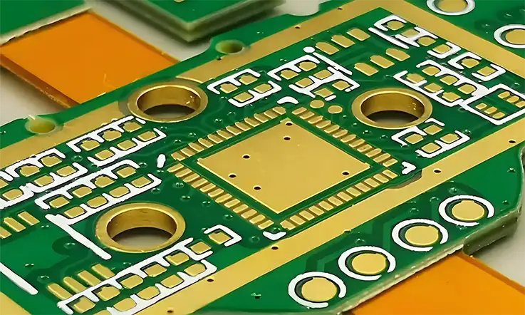
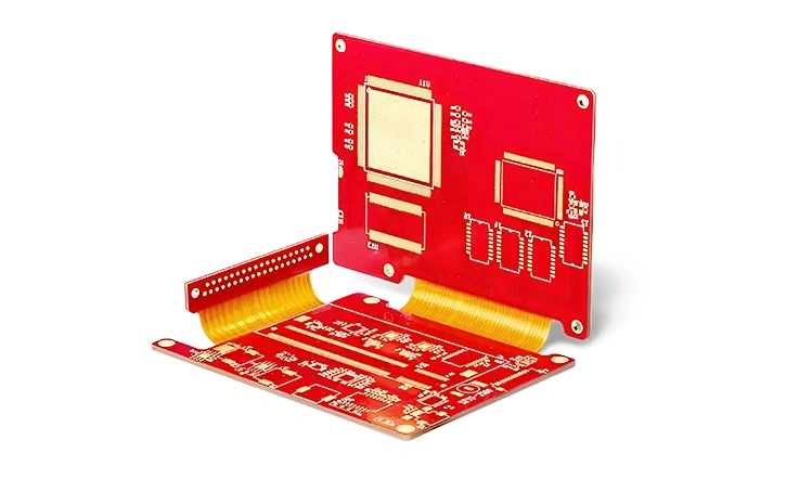
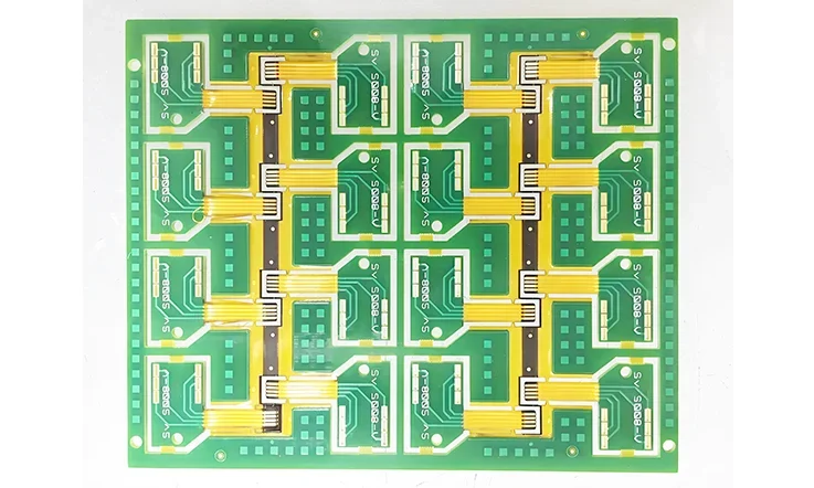
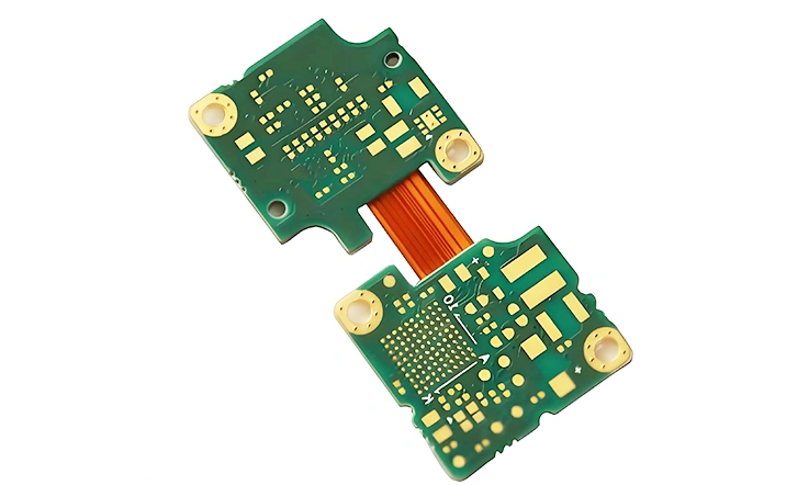
A 14-layer rigid-flex printed circuit board is a hybrid circuit configuration. It combines the dimensional stability of rigid FR-4 sections with the three-dimensional routing capabilities of flexible polyimide-based circuits. The resulting monolithic structure obviates the need for connectors and discrete cables between rigid boards, yielding a more reliable, compact, and lightweight solution for intricate electronic systems.
Core Architecture and Construction
The fundamental architecture of a 14-layer rigid-flex board is realized through the selective lamination of multiple rigid and flexible sub-circuits into a unified stack-up. This intricate process necessitates precise control over materials and manufacturing parameters to manage the inherent mechanical stresses, particularly at the transition zones between rigid and flexible sections, as defined in the IPC-2223 design standard.
●Hybrid Stack-up: The construction involves embedding one or more flexible circuit layers, typically fabricated from polyimide, between multiple layers of rigid FR-4 or similar high-performance laminates.
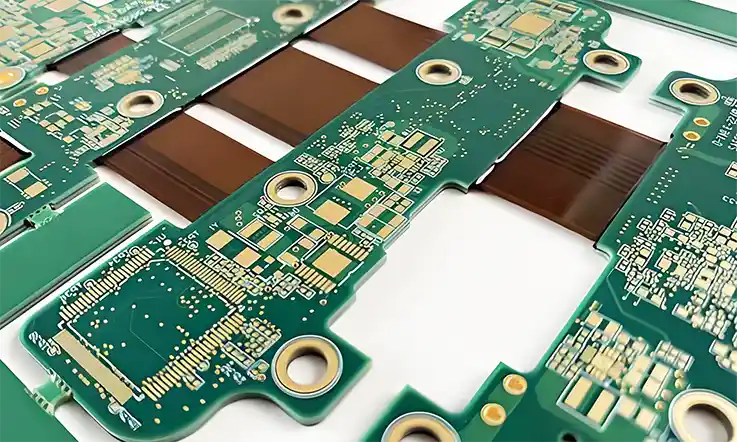
●Monolithic Integration: In contrast to separate boards joined by wires, the entire circuit is fabricated as a single component. This structure facilitates continuous electrical paths that run uninterrupted from rigid sections, through the flex arms, and into other rigid sections.
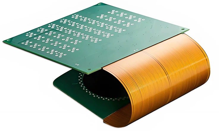
●Three-Dimensional Form Factor: A primary attribute is the capacity to fold the flexible sections to fit into compact and non-planar enclosures, a feat impossible for purely rigid boards. This functionality enables substantial product miniaturization.
●Z-Axis Interconnects: Connections between layers are formed using plated through-holes (PTHs), blind vias, and buried vias. These vertical interconnects must be engineered to withstand the mechanical stresses induced by flexing.
Key Advantages Over Conventional Solutions
Opting for a 14-layer rigid-flex design over a traditional multi-board assembly with cables and connectors offers distinct engineering benefits. These benefits become pronounced in high-stakes applications where system failure carries severe consequences.
●Enhanced Reliability: The elimination of mechanical connectors, which are common points of electromechanical failure, substantially increases overall system reliability. The continuous internal connections are less susceptible to intermittent faults arising from vibration, shock, and thermal cycling.
●Signal Integrity: Shorter, direct signal paths without the impedance discontinuities introduced by connectors lead to superior signal integrity. This has direct implications for the performance of high-speed digital circuits and high-frequency RF applications.
●Space and Weight Reduction: The ability to fold the circuit permits an extremely dense packaging arrangement, significantly reducing the final product’s volume and weight. This is a determining factor in aerospace, medical implant, and portable device design.
●Simplified Assembly Logistics: Although the PCB itself is more complex to fabricate, its use simplifies the final product assembly process. A single board reduces component count, minimizes the potential for manual wiring errors, and streamlines the supply chain.
Applications in Mission-Critical Industries
The unique combination of density, reliability, and form factor makes 14-layer rigid-flex PCBs an enabling technology for many of the world’s advanced electronic systems. They are specified for applications where performance cannot be compromised by environmental or physical constraints.
Aerospace and Defense Systems
In the unforgiving environments of aerospace and defense, where components are subjected to extreme G-forces, temperature swings, and vibration, the inherent robustness of a rigid-flex architecture is a specific design choice for mission continuity.
●Vibration and Shock Resistance: The inherent compliance of the flexible sections absorbs mechanical energy, protecting solder joints and components from fatigue and failure—a common issue in systems mounted on aircraft or tactical vehicles.
●Extreme Temperature Operation: These systems demand materials and construction techniques that can withstand thermal cycles from deep space cold to atmospheric re-entry heat. The material selection and lamination processes are tailored for maximum thermal stability.
●Weight-Sensitive Designs: In any airborne system, from commercial aircraft to unmanned aerial vehicles (UAVs), mass is a primary design constraint. Rigid-flex integration provides the required functionality with the lowest possible mass.
●Mission-Critical Reliability: For guidance, radar, and electronic warfare systems, a single interconnect failure can have catastrophic consequences. The connector-free architecture of rigid-flex boards provides the high level of assurance required for such functions, often demanding qualification to IPC-6013 Class 3 standards.
Medical Devices and Implants
The medical field specifies compact, lightweight, and biocompatible electronics for both diagnostic and implantable devices. The ability of 14-layer rigid-flex designs to conform to the human body while housing complex circuitry is a primary enabler for patient safety and device efficacy.
●Implantable Devices: Pacemakers, defibrillators, cochlear implants, and neurostimulators depend on rigid-flex circuits that can be folded into hermetically sealed, biocompatible enclosures. The operational consistency of these circuits directly affects patient health and safety.
●Surgical Tools and Robotics: Advanced surgical instruments, including endoscopic cameras and robotic surgical arms, use rigid-flex PCBs to route signals and power through tight, articulating joints without cumbersome, failure-prone cables.
●Diagnostic and Wearable Sensors: High-performance wearable health monitors that track vital signs require dense sensor integration in a small, flexible package. Rigid-flex boards enable this by connecting rigid sensor islands with flexible interconnects that can bend with the body.
Industrial Automation and Robotics
Modern industrial automation relies on sophisticated robotics and sensor networks that operate in harsh environments. The combination of repetitive motion and the need for reliable signaling in high-noise factory floors makes rigid-flex a superior choice over conventional wiring.
●Robotic Arms: The repetitive, multi-axis movement of a robotic arm would quickly wear out conventional cables. A custom-designed rigid-flex circuit can endure millions of flex cycles while providing reliable connections for motors, sensors, and actuators.
●High-Density Sensor Heads: Industrial inspection systems often use complex sensor heads with multiple cameras and light sources. A rigid-flex design allows all this technology to be integrated into a compact head, connected by a single flexible tail.
●Harsh Environment Operation: Factory floors are subject to chemical exposure, high temperatures, and significant electrical noise. Rigid-flex boards can be designed with robust materials and shielding to ensure long-term operational integrity in these conditions.
Design for Manufacturability (DFM) for Complex Rigid-Flex Circuits
A successful 14-layer rigid-flex project is not born from a design simply transferred to a fabrication facility. It is forged through a collaborative process centered on Design for Manufacturability (DFM). DFM is a proactive engineering discipline focused on optimizing a design for efficient, repeatable, and high-yield fabrication. Engaging a fabrication entity with deep DFM expertise early in the design cycle is a highly effective action a design group can take to mitigate risk, control costs, and accelerate time-to-market. This approach transforms the relationship into a technical partnership.
The Philosophy of Early Engagement
The core principle of DFM is that the cost of correcting a design flaw increases exponentially as a project moves from concept to production. A modification that takes minutes in a CAD tool can cost thousands of dollars and weeks of delay if discovered only after fabrication tooling has been created. For complex 14-layer rigid-flex boards, this principle is amplified. The DFM process involves a comprehensive review of the design data to identify and resolve potential issues before they can affect fabrication.
●Stack-up and Material Analysis: The proposed layer stack-up is analyzed to confirm it is manufacturable and thermally stable. Alternative materials or a different layer arrangement may be suggested to improve impedance control, reduce warpage risk, or lower cost without compromising performance.
●Transition Zone Optimization: The rigid-to-flex interface is a notorious point of failure if not designed correctly. The DFM review scrutinizes trace routing, via placement, and ground plane continuity in these zones to eliminate stress concentrators and ensure long-term reliability.
●Bend Radius and Flex Life Validation: Designers may specify bend radii that are too aggressive for the chosen materials. These specifications are validated against material properties and the number of layers in the flex section. For example, a static bend radius may need to be at least 10 times the flex section thickness, while a dynamic bend may require 20 to 40 times the thickness.
●Component and Feature Checks: Software tools automatically check for manufacturability violations, such as acid traps, solder mask slivers, insufficient annular rings, or components placed too close to bend lines. Identifying these issues early prevents yield loss and reliability problems.
DFM as a Cost-Control Tool
While DFM is primarily about ensuring reliability, it is also one of the most effective cost-control methodologies. By optimizing a design for specific fabrication processes, yield can be maximized and waste can be minimized, which directly translates to a lower per-unit cost.
●Tolerance Harmonization: Engineers work together to establish tolerances that are achievable and cost-effective. Unnecessarily tight tolerances are a major cost driver. The DFM process identifies where tolerances can be relaxed without affecting function, and where they must be held tight.
●Panelization Strategy: Expert guidance can be provided on arranging a board on production panels. An efficient panel layout maximizes the use of expensive high-performance materials and reduces machining time, significantly affecting the final price.
●Via Technology Optimization: A DFM review can often identify opportunities to replace costly stacked microvias with more manufacturable staggered vias or even conventional through-holes without affecting routing density, leading to substantial cost savings.
Material Science for High-Performance Rigid-Flex PCBs
The selection of materials for a 14-layer rigid-flex PCB is one of the most consequential decisions in the design process. The interplay between dielectrics, adhesives, and conductive foils, as specified in standards like IPC-4101 (for rigid laminates) and IPC-4202/4204 (for flexible dielectrics), dictates the board’s electrical performance, mechanical durability, and its ability to survive the rigors of fabrication and assembly.
Dielectric Core and Prepreg Materials
The dielectric materials form the insulating structure of the PCB. In a rigid-flex design, their properties must be carefully matched between the rigid and flexible sections to ensure thermal and mechanical stability throughout the board’s operational life.
| Material Type | Application Area | Typical Tg (°C) | CTE (ppm/°C) | Flex Cycles |
| Polyimide (PI) | Flex Core | >250 | ~20 | >100,000 |
| FR-4 Standard | Rigid Core | 130–140 | ~70 | N/A |
| FR-4 High-Tg | Rigid Core | >170 | ~55 | N/A |
| Adhesive-Based Flex | Flex Core (legacy) | ~200 | >120 | <10,000 |
| Adhesiveless PI | Flex Core (modern) | >250 | ~20 | >100,000 |
●Polyimide (PI) for Flex Cores: Polyimide is the industry standard for flexible circuits due to its excellent thermal stability, chemical resistance, and outstanding mechanical flexibility. It can withstand the high temperatures of soldering processes (often exceeding 260°C) and maintain its properties over thousands of bend cycles.
●FR-4 and High-Tg Laminates for Rigid Cores: The rigid sections are typically built using standard FR-4. For applications requiring higher thermal performance, high-Tg FR-4 (with a glass transition temperature, Tg, exceeding 170°C) or other advanced laminates like polyimide or cyanate ester are used to prevent the board from becoming unstable at elevated temperatures.
●Adhesiveless vs. Adhesive-Based Flex Cores: Traditional flex circuits used acrylic or epoxy adhesives to bond the copper foil to the polyimide core. Modern high-performance designs, however, increasingly use adhesiveless base materials, where the copper is deposited directly onto the polyimide. This eliminates the high-CTE adhesive layer, resulting in thinner, more flexible circuits with improved dimensional stability and higher thermal reliability.
Conductive Copper Foils
The type of copper foil used in rigid and flexible sections differs based on the mechanical demands placed upon it. Using a non-optimal type of copper is a common design flaw that can lead to premature circuit failure under dynamic stress.
●Electro-Deposited (ED) Copper: This type of copper is most common in rigid boards. It has a vertical grain structure, which provides good electrical conductivity and adhesion but is relatively brittle, rendering it unsuitable for dynamic flexing.
●Rolled-Annealed (RA) Copper: RA foil is specifically manufactured for flexible circuits. It has an elongated, horizontal grain structure that gives it superior ductility and fatigue resistance. It can withstand repeated bending without cracking, making it a mandatory choice for the flex sections of a rigid-flex board.
●Copper Weight and Distribution: The thickness of the copper foil (measured in ounces per square foot, e.g., 0.5 oz, 1.0 oz, or 2.0 oz) must be carefully selected to meet current-carrying requirements while also considering its impact on flexibility. Heavier copper makes the circuit stiffer and reduces its flex life. Balancing copper distribution across all layers is also a prerequisite to prevent board warpage.
Bonding Systems: Adhesives and Coverlays
The materials used to bond the layers together and to protect the outer surfaces of the flex circuits govern the board’s long-term integrity. The choice of these materials directly affects how well the board withstands lamination, assembly, and real-world environmental stresses.
| Material | Function | Thickness Range (mm) | Thermal Stability (°C) | Used In |
| FR-4 Prepreg | Lamination of rigid cores | 0.075–0.25 | Up to 150 | Rigid sections |
| No-Flow Prepreg | Prevent resin seepage | 0.1–0.2 | Up to 170 | Rigid-flex interface |
| Bondply Adhesive | Flex-to-rigid bond layer | 0.05–0.125 | Up to 180 | Transition zones |
| PI Coverlay Film | Surface protection on flex | 0.025–0.05 (film only) | Up to 250 | External flex sides |
●Prepreg: In the rigid sections, layers are bonded together using “prepreg“—a woven glass fabric impregnated with partially cured epoxy resin. During lamination, heat and pressure fully cure the resin, fusing the layers together. Low-flow or no-flow prepregs are often used at the rigid-flex interface to prevent resin from seeping into the flexible areas.
●Bondply and Adhesives: To bond the rigid and flexible sections together, specialized flexible adhesives like bondplies (adhesive films with a supporting carrier) are employed. These must provide a strong bond while remaining compliant enough to manage CTE mismatches.
●Coverlay: The outer surfaces of the flex circuits are protected by a coverlay, which is a layer of polyimide film with an adhesive backing. It serves the same function as soldermask on a rigid board—insulating the copper traces and protecting them from the environment, while leaving pads open for component assembly.
Thermal Management in Dense Rigid-Flex Systems
As component densities, clock speeds, and power requirements escalate within the compact confines of a 14-layer rigid-flex board, effective thermal management becomes a first-order engineering challenge. Heat is a primary adversary of electronic reliability, degrading component performance and lifespan. A proactive thermal management strategy, engineered directly into the PCB structure, is a prerequisite for success in high-performance applications. This requires a deep understanding of heat transfer principles within the unique, heterogeneous material set of a rigid-flex design.
The Unique Thermal Challenge in Rigid-Flex
Unlike a homogenous rigid board, a rigid-flex PCB presents a complex thermal landscape. The core material of the flexible sections, polyimide, is an excellent electrical insulator but also a poor thermal conductor. This creates potential thermal “bottlenecks,” where heat generated by powerful components on a rigid section struggles to dissipate across the thin flex arms. This can lead to localized hotspots that can degrade signal integrity, accelerate material aging, and cause premature component failure. A sophisticated approach is needed to create efficient thermal pathways through this complex structure.
Identifying Hotspots:
The first step is to use thermal simulation software, often integrated with the ECAD tool, to identify potential hotspots under various operating conditions. This analysis guides the entire thermal management strategy.
Understanding Thermal Resistance:
Every material in the stack-up has a specific thermal resistance. The objective is to create a low-resistance path for heat to travel from the component junction to the ambient environment. This involves leveraging the most thermally conductive materials in the stack-up: copper.
Managing CTE Mismatch:
Aggressive thermal solutions, like embedding metal coins, can introduce significant Coefficient of Thermal Expansion (CTE) mismatches. These must be carefully managed with compliant bonding materials and design rules to prevent delamination or via cracking during thermal cycling.
Engineering Effective Thermal Pathways
A suite of advanced techniques can be employed to actively manage heat within the PCB, turning the board itself into a component of the thermal solution.
Thermal Via Arrays:
This technique is a common and effective method for drawing heat vertically through the board. A grid of plated through-holes is placed directly under a heat-generating component. These vias act as highly efficient thermal pipes, conducting heat from the component’s thermal pad down into internal copper planes or to a heat sink on the opposing side. The effectiveness is a function of via diameter, plating thickness, pitch, and whether they are filled with thermally conductive paste.
Heavy Copper Planes and Pours:
Incorporating one or more solid, heavy copper layers (e.g., 2 oz, 3 oz, or heavier) into the stack-up provides an excellent lateral heat spreading path. These planes draw heat away from a concentrated source and distribute it over a much larger area, significantly reducing the peak temperature.
Embedded Thermal Coins:
For the most extreme power dissipation requirements (e.g., high-power FPGAs or power amplifiers), a solid copper or aluminum “coin” can be embedded into a cutout within the PCB layers. The component is mounted directly onto this coin, creating the lowest possible thermal resistance path to an external chassis or heat sink. This is a complex process involving multiple lamination and plating steps that showcases a high level of fabrication capability.
Thermally Conductive Dielectrics:
While standard FR-4 and polyimide are thermal insulators, specialized dielectric materials are available. These materials are filled with ceramic particles (like alumina or boron nitride) that significantly increase their thermal conductivity. Strategically using these materials in the rigid sections of the stack-up can improve heat transfer away from critical components without relying solely on copper.
Interconnect Strategies: Vias and Sequential Lamination
In a dense 14-layer structure, vias are not just simple connections; they are engineered features that define the board’s routability and reliability. A sophisticated via strategy allows for escaping dense components like BGAs and maintaining robust connections through multiple lamination cycles and mechanical stresses.
Blind, Buried, and Microvia Technologies
To achieve the high routing density required in modern electronics, designers leverage advanced via structures. These specialized vias do not pass through the entire board, freeing up valuable real estate on other layers for signal routing.
●Buried Vias: These are plated holes that connect only internal layers of the PCB. They are drilled and plated in a sub-assembly of layers before being laminated inside the final board. They are completely invisible from the outside of the finished PCB.
●Blind Vias: These are plated holes that connect an external layer to one or more internal layers, but do not go all the way through the board. They are drilled with precisely controlled depth, either mechanically or with a laser.
●Microvias (μVias): These are typically laser-drilled blind vias with a very small diameter (usually less than 150 μm, with advanced processes achieving diameters down to 75 μm). They are a feature of High-Density Interconnect (HDI) designs, allowing for via-in-pad (VIP) technology and enabling routing escape from fine-pitch BGAs. In rigid-flex boards, microvias require extremely precise registration control through multiple lamination cycles.
Via Types and Feature Summary:
| Via Type | Connection Layers | Diameter (μm) | Fabrication Method | Used In |
| Buried | Internal–Internal | 200–350 | Mechanical Drilling | Inner Core Routing |
| Blind | Outer–Internal | 150–300 | Laser / Mechanical | BGA Escape |
| Microvia (μVia) | Single-Layer Only | 75–150 | Laser Drilling | HDI / VIP Routing |
Sequential Lamination and Stacked Vias
Building a board with blind and buried vias is not possible with a single lamination press cycle. This requires a process called sequential lamination, where subsets of layers are fabricated and then laminated together in stages, adding significant complexity and cost.
Multi-Stage Lamination:
A 14-layer board with advanced vias might be built in two, three, or even more lamination cycles. For example, layers 7-8 may be laminated to form a core with buried vias. Then, layers 5-6 and 9-10 are added in a second cycle, with blind microvias drilled down to the inner core. Finally, the outer layers are added in a third cycle.
Stacked and Staggered Microvias:
Microvias can be “stacked” directly on top of each other across multiple layers or “staggered” in an offset pattern. Stacked microvias require a specialized process where each via is filled with conductive paste or plated shut before the next layer is added, ensuring a reliable connection. This is the most space-efficient but also the most complex and costly approach.
Aspect Ratio Considerations:
The aspect ratio of a via—the ratio of its depth to its diameter—is a determining factor for reliable plating. For through-hole vias in a 14-layer board, this ratio can easily exceed 10:1. Deep, narrow holes are difficult to plate evenly. The available process controls must be optimized to achieve reliable plating even in high aspect ratio through-holes.
Sequential Lamination and Stacked Microvia Complexity:
| Build Type | Lamination Cycles | Via Strategy | Fabrication Risk | Cost Tier |
| Single Lamination | 1 | Through-Hole Only | Low | Low |
| Dual Lamination | 2 | Blind + Buried | Medium | Medium |
| Triple Lamination (HDI) | 3 | Stacked Microvia + VIP | High | High |
Typical Aspect Ratios by Via Type:
| Via Type | Depth (mm) | Diameter (mm) | Aspect Ratio |
| Through-Hole | 1.6–2.0 | 0.2 | 8:1 – 10:1 |
| Blind Microvia | 0.1–0.2 | 0.1 | 1:1 – 2:1 |
| Stacked μVias | 0.2 × 3 steps | 0.1 | 6:1 combined |
EMI and EMC Shielding for High-Frequency Circuits
In the dense, high-speed environment of a 14-layer rigid-flex PCB, every trace can act as a miniature antenna. This creates a significant challenge for Electromagnetic Interference (EMI) and Electromagnetic Compatibility (EMC). A board must not only function correctly itself, but must do so without radiating noise that disrupts adjacent systems (EMI) and without being susceptible to external noise that could corrupt its own signals (EMC). For mission-critical applications in aerospace, medical, and defense, achieving robust EMC performance must be designed in from the start.
The Principles of Electromagnetic Shielding
Effective shielding in a PCB works by controlling electromagnetic fields. This is accomplished through two primary mechanisms: containing internally generated fields from sources like high-speed clock lines, and blocking externally generated fields from penetrating the board and affecting sensitive circuits.
●Source Containment: The most effective strategy is to contain noise at its source. This involves careful routing of high-speed signals and providing an immediate, low-impedance return path for their currents.
●Victim Protection: For highly sensitive circuits, such as low-noise amplifiers or analog-to-digital converters, the goal is to create a “quiet” zone, shielding them from noise generated by other parts of the board or from the external environment.
●Grounding Strategy: A well-designed grounding scheme is the foundation of all shielding. A single, unified ground plane with low impedance is necessary. Any splits or gaps in the ground plane can create “slots” that radiate EMI like an antenna.
Shielding Methodologies for Rigid-Flex PCBs
A multi-faceted approach to shielding can be implemented, integrating it directly into the board’s structure to provide comprehensive protection across both rigid and flexible sections.
Solid Ground Planes (Faraday Cages):
The most fundamental shielding technique is the use of solid copper planes. Dedicating entire layers of the 14-layer stack-up to be uninterrupted ground planes creates a Faraday cage effect. Traces routed on an internal layer between two solid ground planes (a stripline configuration) are exceptionally well-shielded from both emitting and receiving interference.
Guard Traces and Via Fencing:
For critical signals routed on outer layers (microstrip), a “guard trace” connected to ground can be routed parallel to the signal trace. This helps contain the signal’s electric fields. This technique is often enhanced by creating a “via fence”—a row of ground-connected vias stitched along the edge of the trace—which forms a vertical grounded wall to further confine the electromagnetic fields.
Specialized Shielding Films for Flex:
The flexible sections present a unique challenge, as adding solid copper planes would destroy their flexibility. For these areas, specialized shielding films are utilized. These are thin, flexible polyimide films with a conductive layer applied to them, often a cross-hatched silver ink pattern or a sputtered layer of copper/nickel. These films are laminated onto the exterior of the flex circuit, providing effective EMI protection with minimal impact on bendability.
Cross-Hatched vs. Solid Fills:
In large copper pour areas used for shielding, a solid fill provides the best shielding effectiveness but can sometimes cause processing issues or add unwanted stiffness in flex areas. A cross-hatched or mesh pattern can be used as a compromise, offering good shielding while improving flexibility and adhesion. The design of the mesh grid is managed to avoid creating resonant slots at frequencies of interest.
Surface Finishes: Impact on Assembly and Reliability
The surface finish is the final coating applied to exposed copper pads on a PCB. It is a material interface that serves two primary purposes: protecting the copper from oxidation and providing a solderable surface for component assembly. In a complex rigid-flex board, the choice of surface finish has significant implications for assembly yield, long-term reliability, and cost.
Comparing Common Surface Finishes
Different finishes have distinct attributes and are suited for different applications and cost targets. The selection of an optimal finish is an engineering decision based on the design’s specific performance and reliability requirements.
●ENIG (Electroless Nickel Immersion Gold): This is one of the most frequently specified finishes for high-reliability applications. It features a layer of nickel (3-6 μm thick), which acts as a diffusion barrier, covered by a thin layer of immersion gold (0.05-0.1 μm) for protection and solderability. It provides a very flat (planar) surface, making it suitable for fine-pitch BGAs, and has a long shelf life.
●ENEPIG (Electroless Nickel Electroless Palladium Immersion Gold): An enhancement of ENIG, ENEPIG adds a layer of palladium between the nickel and gold. The palladium layer prevents potential “black pad” syndrome (a corrosion issue with ENIG) and provides an excellent surface for gold wire bonding, making it a top choice for the most demanding applications.
●Immersion Silver (ImAg): This finish offers excellent planarity and a highly solderable surface at a lower cost than gold-based finishes. It is, however, susceptible to tarnishing and requires more careful handling and storage. It is a reliable choice for high-speed circuits due to its low signal loss.
●OSP (Organic Solderability Preservative): OSP is a very thin, organic coating that protects the copper before soldering. It is the most cost-effective and environmentally friendly option. It has a limited shelf life, can only withstand a few reflow cycles, and is not suitable for wire bonding.
Considerations for Rigid-Flex Applications
The unique nature of rigid-flex boards introduces special considerations when selecting a surface finish. The chosen finish must not only perform electrically but also survive the mechanical stresses inherent in a flexible design.
●Flexibility and Adhesion: The surface finish applied to the flexible arms of the board must be able to withstand bending without cracking or flaking. Gold-based finishes like ENIG and ENEPIG generally have excellent ductility and adhere well to the flexible polyimide substrate.
●Mixed Finishes: In some advanced designs, it may be desirable to have different finishes on different parts of the board. For example, ENIG might be used on the rigid sections for BGA mounting, while a more flexible finish is used on the dynamic flex areas. This requires a selective finishing process, which adds complexity and cost but can optimize performance.
●Connector Pad Durability: For edge connectors or card fingers that will undergo repeated insertions, a “hard gold” finish is often required. This involves electroplating a thick layer of gold over a nickel barrier, providing a durable, wear-resistant surface. This is a separate process that can be combined with other finishes on the board.
Assembly (PCBA) of Complex Rigid-Flex Boards
Assembling components onto a 14-layer rigid-flex PCB is significantly more challenging than assembling a standard rigid board. The mixed materials, uneven topography, and inherent flexibility of the board require specialized equipment, processes, and expertise adhering to standards like IPC-A-610 and J-STD-001 to achieve high yields and long-term reliability.
Specialized Fixturing and Handling
Unlike rigid boards that can be placed directly onto a conveyor, flexible and rigid-flex boards require custom fixtures or pallets. These tools are necessary to hold the board flat and stable throughout the entire automated assembly process.
●Reflow Pallets: Custom-machined pallets, often made from high-temperature composite materials, are designed to support the board during screen printing of solder paste and the reflow soldering process. The pallet ensures the board remains perfectly flat, a condition for consistent solder paste deposition and preventing component shift during reflow.
●Support for 3D Shapes: For boards that are already folded into a 3D shape before assembly, highly complex, multi-part fixtures are needed to hold the board securely during component placement and soldering.
●ESD and Handling Protocols: The flexible sections are sensitive to handling damage. Strict ESD (electrostatic discharge) and handling protocols must be in place to prevent both electrical damage and physical creasing or tearing of the flex circuits.
Underfill, Conformal Coating, and Encapsulation
For high-reliability applications, post-assembly processes are often required to protect the components and solder joints from mechanical stress, moisture, and other environmental factors. These protective layers are specified to ensure the product survives its intended operating environment.
●Underfill: For large BGA components, an epoxy “underfill” is often dispensed under the package after it has been soldered. The underfill fills the gap between the BGA and the PCB, mechanically reinforcing the fragile solder balls and substantially improving their reliability under shock, vibration, and thermal cycling.
●Conformal Coating: A thin, polymeric film is applied over the entire assembled board to protect it from moisture, dust, and chemicals. There are various types of conformal coating (acrylic, silicone, urethane), and the selection depends on the application’s operating environment. Applying it evenly on a complex 3D rigid-flex assembly requires specialized robotic spraying or dipping processes.
●Encapsulation (Potting): For extreme protection, parts of the board or the entire assembly can be encapsulated in a solid block of epoxy or silicone resin. This provides the ultimate protection against mechanical shock and fluid ingress but makes repair impossible.
Post-Assembly Cleaning and Inspection
Cleaning flux residues and inspecting the final assembly present unique challenges on a rigid-flex board due to its complex geometry. Failure to properly clean and inspect can lead to latent field failures.
●Cleaning Challenges: Aggressive cleaning solvents or high-pressure sprays can damage the flexible sections or the materials used in their construction. Specialized, material-compatible cleaning processes must be used to remove flux residues without compromising the board’s integrity.
●3D Automated Optical Inspection (AOI): Standard 2D AOI systems may struggle with the varying topography of a rigid-flex board. 3D AOI systems are used to accurately inspect solder joint quality on components at different heights and on different sections of the board, comparing results against IPC-A-610 Class 3 criteria.
●X-Ray Inspection: For BGA and other bottom-terminated components, 2D and 3D (CT) X-ray inspection is a necessity to verify solder joint integrity, check for voids, and ensure there are no shorts underneath the package.
Cost Drivers for Rigid-Flex PCB Fabrication
While 14-layer rigid-flex PCBs offer unparalleled performance and integration, they represent a significant investment. Understanding the key factors that drive cost is a prerequisite for optimizing a design to meet both technical and budgetary targets. A collaborative engineering approach is the most effective way to manage these costs.
Material Choices and Layer Count
The raw materials and the sheer complexity of the stack-up are the most significant contributors to the final cost. These choices form the baseline price before any fabrication processes are considered.
| Item | Option | Cost Impact |
| Rigid Core | Standard FR-4 | Low |
| High-Tg FR-4 / Polyimide | Medium–High | |
| Flex Core | Adhesive-Based Polyimide | Medium |
| Adhesiveless Polyimide | High | |
| RF/Mixed-Signal Layers | Low-Dk / Thermally Stable | Very High |
| Layer Count | ≤8 | Baseline |
| 14+ | +2.5–3.2× | |
| Copper Weight | 1 oz | Standard |
| 2 oz+ | +20–40% |
●High-Performance Materials: While standard FR-4 and polyimide are the baseline, opting for high-Tg materials, low-loss RF laminates, or thermally conductive dielectrics will increase the material cost. Adhesiveless flex cores are more expensive than their adhesive-based counterparts but offer higher reliability.
●Layer Count and Lamination Cycles: Cost increases non-linearly with layer count. A 14-layer board is substantially more than twice the cost of a 7-layer board because each additional layer adds material, processing steps, and lamination cycles. Boards requiring multiple sequential lamination cycles for advanced vias are markedly more expensive.
●Copper Weight: Using heavier copper (e.g., 2 oz or more) for power layers increases material cost and can make processing more difficult, affecting yield and therefore price.
Design Complexity and Tolerances
The intricacy of the design and the tightness of the required tolerances have a direct impact on fabrication yield. Lower yields due to high complexity translate directly into higher per-unit costs.
| Design Feature | Threshold | Cost Trend |
| Trace/Space | < 75μm (3 mil) | +15–25% |
| Via Type | Blind/Buried/Microvia | +30–120% |
| Impedance Control | ±10% | Standard |
| ±5% | +5–12% |
●Trace and Space Dimensions: Designs that push the limits of trace width and spacing (e.g., below 75 microns / 3 mils) require more advanced equipment and tighter process controls, leading to lower yields and higher costs.
●Via Technology: A simple through-hole design is the most cost-effective. The introduction of blind, buried, and especially stacked, filled microvias dramatically increases the number of process steps (drilling, plating, filling, lamination) and drives up the price.
●Tolerances: Demanding very tight tolerances on hole positions, board outline, or impedance control (e.g., ±5% vs. a standard ±10%) requires more process monitoring and may result in a higher scrap rate, which is factored into the final cost.
Panelization, Quantity, and Testing
Fabrication logistics and testing requirements affect the final price. These factors are related to the efficiency of the production run and the level of quality assurance required.
| Factor | Condition | Cost Result |
| Panel Utilization | < 60% | ↑ Material Waste |
| Order Quantity | < 10 pcs | High Setup Cost |
| > 100 pcs | Cost per Unit ↓↓ | |
| Test Method | Flying Probe | Included |
| TDR / Flex-Life / IST | +3–10% |
●Panel Utilization: The objective is to fit as many boards as possible onto a standard production panel to maximize material usage. Awkward shapes or inefficient layouts that waste panel space will increase the cost per board. Expert guidance on panelization can optimize for material efficiency.
●Order Quantity: PCB fabrication involves significant setup costs (tooling, programming). For very small prototype runs, these setup costs dominate the price. As the order quantity increases, these costs are amortized over more units, and the per-board price drops significantly.
●Testing and Qualification: Basic electrical testing (flying probe) is standard. If the design requires more extensive testing—such as impedance TDR measurements, Interconnect Stress Testing (IST), or specific flex-life qualification—these add cost but provide a higher level of quality assurance, reducing the total cost of ownership by preventing field failures.
Evaluating a Superior Fabrication Partner: Key Benchmarks for Success
The selection of an entity for the fabrication and assembly of 14-layer rigid-flex circuits extends beyond a simple purchasing decision; it is an investment in capability and reliability that directly affects the final product’s performance and time-to-market. A discerning evaluation process looks beyond surface-level quotes to assess a potential supplier against a set of rigorous benchmarks.
1. Quality Systems and In-Process Verification
A commitment to quality is evidenced not by claims, but by a deeply integrated and certified quality management system (QMS).
●Certifications as Proof: Look for internationally recognized certifications that are relevant to the application’s end market. ISO 9001 provides a baseline for process control, while more demanding standards like AS9100 (for aerospace and defense) or ISO 13485 (for medical devices) demonstrate a higher level of discipline and traceability.
●Process Control and Traceability: A superior entity maintains meticulous records for traceability throughout the fabrication cycle. This includes tracking material batches, process parameters, and inspection results for every board produced.
●In-house Testing and Inspection: The capability to perform extensive in-house testing is a hallmark of a quality-focused organization. This includes 100% electrical testing (flying probe or bed-of-nails), Automatic Optical Inspection (AOI) at multiple stages, and advanced inspection like 3D X-ray for BGA and complex assemblies. Qualification should be performed against the stringent criteria of IPC-6013 Class 3.
2. Manufacturing Capabilities and Technological Depth
The ability to successfully produce complex, high-layer-count rigid-flex boards requires significant investment in advanced equipment and process engineering expertise.
●Advanced HDI and Via Technology: Assess the entity’s demonstrated capabilities in High-Density Interconnect (HDI) fabrication. This includes their proficiency with sequential lamination, creating stacked or staggered microvias (typically < 100 μm), and their process for via-filling and plating, all of which are fundamental to high-density designs.
●Material Expertise: The organization should possess deep knowledge in handling a wide range of standard and exotic materials, from high-Tg laminates and polyimide films to specialized RF substrates and thermally conductive dielectrics.
●Integrated Fabrication and Assembly: The capacity to handle both bare board fabrication and complex component assembly (PCBA) within a single facility is a substantial advantage. This integrated model eliminates multi-vendor coordination issues, reduces lead times, and ensures that the board is designed from the outset with assembly challenges in mind, a philosophy known as Design for Assembly (DFA).
3. Engineering and Technical Services
A transactional supplier simply executes a command; an engineering-centric organization contributes to the success of the design itself.
●Proactive DFM/DFA Support: Before any fabrication begins, a thorough Design for Manufacturability (DFM) and Design for Assembly (DFA) analysis should be a standard procedure. This process should yield actionable feedback to the designer, aimed at improving yield, enhancing reliability, and reducing cost.
●Stack-up and Impedance Modeling: The entity should provide expert support in designing the PCB stack-up and performing pre-layout impedance modeling to ensure signal integrity requirements are met. This service prevents costly design revisions after the layout is complete.
●Accessibility to Engineers: Direct access to experienced process and layout engineers for technical consultations is a sign of a collaborative and solution-oriented organization.
4. Lead Time, Logistics, and Economic Efficiency
In today’s market, speed and efficiency are as valuable as technical execution.
●Transparent Quoting and Lead Times: The quoting process should be clear, detailed, and provide realistic, achievable lead times. Hidden fees or consistently missed deadlines are indicators of poor operational control.
●Value over Price: The most astute evaluation focuses on Total Cost of Ownership (TCO) rather than the lowest initial per-unit price. A slightly higher initial price from a high-yield, high-reliability supplier often results in a lower TCO by eliminating the costs associated with board failures, project delays, and field returns.
●Flexible Volume Support: The organization should have the logistical framework to support a project’s entire lifecycle, from rapid-turn prototypes in small quantities to scaled-up, high-volume orders.
By evaluating potential suppliers against these comprehensive benchmarks, a clear picture of their true capabilities emerges, enabling an informed decision that aligns with the demanding nature of a 14-layer rigid-flex PCB project.
FAQ for 14-Layer Rigid-Flex PCBs
1. What is the typical lead time for a 14-layer rigid-flex prototype?
Prototype lead times are typically 3-5 weeks, varying with stack-up complexity and material availability. Please submit your design for a firm schedule.
2. Beyond Gerbers, what other files are needed for an accurate fabrication quote?
For an accurate quote, provide Gerbers or ODB++, a detailed stack-up, a fabrication drawing, and a drill table. We also accept modern single-file formats like IPC-2581.
3. Do you offer full turnkey assembly, including component sourcing and management?
Yes, we offer full turnkey solutions. Our service includes component sourcing, fabrication, and final assembly, providing you with a streamlined supply chain and a single point of accountability.
4. What are the best practices for panelizing rigid-flex designs for assembly?
For assembly stability, best practices include using breakaway tabs and v-scoring only on rigid sections, and adding global fiducials and tooling strips to the panel frame.
5. Do you support small-run prototypes before committing to volume production?
Yes, we support projects from prototype to production. Prototyping allows you to validate your design and assembly process before committing to mass production tooling.


