
This guide provides a comprehensive overview of 4-layer rigid-flex PCBs, covering the essentials from design and materials to manufacturing and assembly. It explores the critical technical details, best practices, and advanced concepts required to engineer and produce reliable, high-performance circuits for modern electronics. The following sections delve into the specific knowledge needed to transform a design concept into a functional and durable final product.
Understanding the 4-Layer Rigid-Flex PCB: What It Is and How It’s Built?
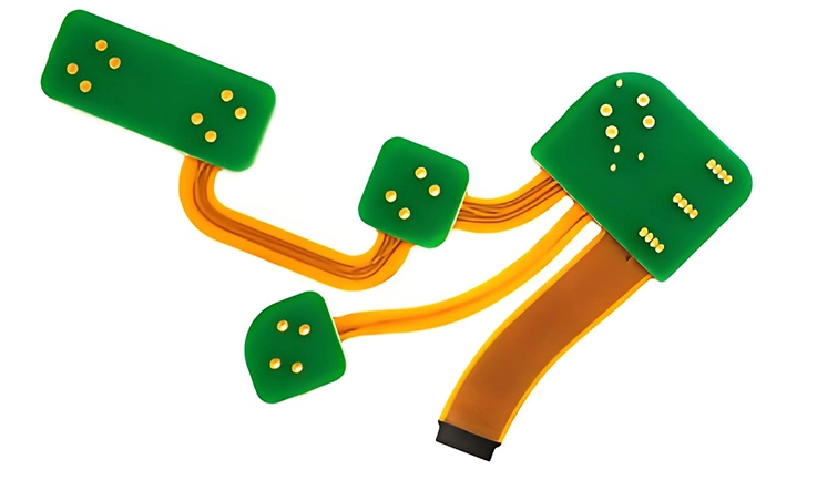
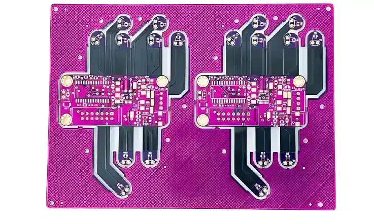
A 4-layer rigid-flex PCB is a sophisticated circuit structure that merges the mechanical stability of rigid boards with the dynamic adaptability of flexible circuits. This unique construction is foundational for creating compact, three-dimensional electronic assemblies that are impossible to achieve with conventional boards alone.
What It Is and How It’s Built?
At its core, a 4-layer rigid-flex PCB is a unified system, not a simple assembly of separate parts. It integrates rigid and flexible substrates into a single, cohesive structure during the manufacturing process. This allows for dense, three-dimensional circuit layouts in compact products, all while maintaining electrical precision. In high-density applications such as consumer electronics, communication modules, and wearable devices, this configuration provides a degree of design freedom and layout compression unachievable with traditional rigid-only boards.
●Unified Fabrication: These boards are not separate pieces assembled after the fact; they are fabricated as unified, multi-region systems.
●Precise Material Bonding: The construction involves a precise sequence of materials bonded into a single, cohesive board, including external rigid layers of FR-4, internal flexible layers of polyimide, selective adhesives, and a protective coverlay.
●Integrated Interconnects: During manufacturing, lamination, drilling, and plating techniques are fine-tuned for each design. Unlike multi-board setups that depend on connectors and cables, a rigid-flex layout removes the need for these secondary interconnects entirely, resulting in a more robust system with fewer potential failure points.
Advantages Over Traditional Board Designs
The architecture of 4-layer rigid-flex PCBs provides distinct functional and mechanical benefits, making them a superior choice for products that demand complex geometries, weight reduction, and high-performance signaling.
●Reduced Space and Weight: By eliminating connectors, jumpers, and separate boards, the architecture is inherently compact. This can reduce the interconnect volume by up to 70% and weight by over 50% compared to using traditional cables and connectors.
●Enhanced Mechanical Design: Boards can be shaped and folded to fit 3D contours inside a product’s housing. This capability supports designs where some components must remain static while flexible arms permit dynamic movement, such as in a hinged device.
●Improved Electrical Reliability: Electrical interconnects are continuous between rigid and flex sections. With no breaks or solder joints between them, issues like extra contact resistance vanish. This directly supports applications with high data transfer rates or sensitivity to power delivery fluctuations.
●Streamlined Assembly: The board is produced as a single, complete unit, which eliminates the step of aligning and connecting separate PCBs. This inherently reduces misalignment risks by up to 100% during final product assembly and simplifies the supply chain.
Typical Applications in Modern Electronics
The adoption of 4-layer rigid-flex PCBs is integral to next-generation products across multiple sectors, particularly those that demand miniaturization without a performance trade-off. They enable functionality that would otherwise be impractical or unreliable.
●Consumer Electronics: Foldable smartphones, AR/VR headsets, and compact cameras leverage these boards to connect antennas, batteries, and logic units into a single folded stack, avoiding bulky and failure-prone internal cabling.
●Wearable Devices: Fitness bands and biometric monitors benefit from flexible routing that wraps around body contours, using the multi-layer structure to integrate sensors, wireless modules, and power sources in an ultra-compact form factor.
●Telecom Modules: Miniaturized wireless units and high-frequency RF boards utilize the controlled impedance of rigid-flex stack-ups to support fast, clean signal transfer, especially where multiple antennas or shielded zones are required.
●Medical Devices: Catheter-based instruments, implantable monitors, and handheld diagnostic tools use flex arms to enable movement and articulation without stressing the electronic connections, a main factor for patient safety and device longevity.
Common 4-Layer Rigid-Flex PCB Stack-up Structures
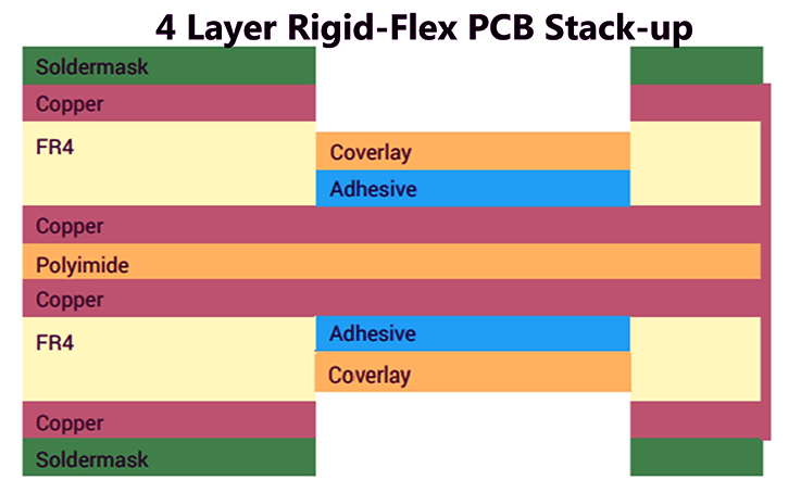
In 4-layer rigid-flex setups, the stack-up arrangement determines how the board handles both signal behavior and physical strain. The specific layering of signal, power, and ground conductors shapes impedance tuning, manages unwanted interference, and helps maintain balance between the rigid and flexible zones. This layering becomes especially relevant when combining polyimide (PI) with FR-4, as each responds differently under thermal cycles and mechanical movement.
Arranging Signal and Power Layers
The strategic layout of signal and power layers is fundamental to achieving both electrical performance and physical balance in a 4-layer design. The following configuration is widely adopted for its ability to deliver excellent signal integrity and noise control.
●Top Layer (Layer 1): Typically hosts high-speed signal traces and is often located on the rigid section to minimize fluctuations in dielectric thickness.
●Inner Layer 1 (Layer 2): Acts as a reference plane (ground or power), which enhances signal integrity by providing a clear return path and helps reduce electromagnetic interference (EMI).
●Inner Layer 2 (Layer 3): Supports secondary signals or low-speed control lines, spaced to avoid interference with sensitive paths on other layers.
●Bottom Layer (Layer 4): Often used for power or ground to provide tight return paths for signals on Layer 3 and assist with thermal dispersion across the board.
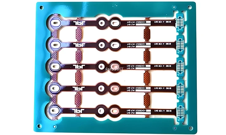
Connecting Layers with Via Structures
Vias are the vertical interconnects that bridge the copper layers, and their design in rigid-flex PCBs must accommodate both static rigid zones and dynamic bending areas. The choice of via technology has a direct impact on routing density and manufacturing complexity.
●Through-Hole Vias: Extend through all layers of the board and are typically located in rigid zones to provide strong mechanical support and robust connections.
●Blind Vias:Connect an outer layer to an internal layer without passing through the entire board, which is useful for freeing up routing space in high-density areas like BGA footprints.
●Buried Vias: Are contained entirely between internal layers, providing connections that do not affect the surface routing on either side of the board, maximizing surface area for components.
●Laser Microvias: Often used in flexible sections, these are formed by laser drilling and allow for thin, lightweight, high-density circuits with extremely fine features, often below 75μm.
Designing the Stack-up for Long-Term Reliability
To enhance the durability of a 4-layer rigid-flex PCB, stack-up decisions must look beyond immediate electrical function to anticipate mechanical and thermal behavior over the product’s lifecycle. These strategies are built into the fabrication process to ensure stability.
●Symmetrical Construction: A balanced distribution of copper weight and dielectric thickness across the stack-up’s central axis reduces the risk of warping or delamination during thermal cycling.
●Controlled Copper Thickness: Using thinner copper (typically ≤1 oz or 35μm) in flex regions improves bend endurance without sacrificing necessary current-carrying capability.
●Precision Coverlay Openings: Strategically placing coverlay windows with smooth, rounded corners prevents stress from concentrating at specific points during flexing, extending the board’s dynamic life.
●Multi-Stage Lamination: Employing gradual temperature and pressure profiles helps manage the CTE mismatch between FR-4 and polyimide, minimizing the chance of delamination at the rigid-flex interface.
Best Practices in 4-Layer Rigid-Flex PCB Design
This section outlines recommended design approaches that help ensure a successful build and dependable performance. Thoughtful decisions during layout and routing influence not only electrical characteristics but also bending endurance, thermal response, and ease of assembly. These design choices stem from direct experience with rigid-flex layer stack-ups, trace routing, and material behavior.
Mechanical Design Considerations
From a fabrication perspective, mechanical stress zones and material transitions require careful planning. These considerations affect how the board is folded, how flex arms behave over time, and whether traces maintain adhesion under repeated strain.
●Maintain Bend Radii: A general rule is to maintain the bend radius at least ten times the thickness of the flex layer (10x) to prevent copper from cracking during bending. For dynamic applications, a radius of 20x or greater is strongly recommended.
●Avoid Traces Crossing Fold Lines: Routing traces perpendicular to a bend area can invite mechanical fatigue. Instead, place traces parallel to the bend or shift the circuitry away from the bend line entirely.
●Use Stress Relief Features: Incorporating teardrops at via pads and using hatched copper planes in flexible areas helps spread mechanical load and reduce stress concentration.
●Limit Component Placement Near Flex Hinges: Rigid sections should host surface-mount devices and connectors. Flex arms should remain free of components to preserve their full dynamic bending tolerance.
Layer-to-Layer Transition Rules
Moving from rigid zones into flex areas involves changes in layer thickness, dielectric materials, and copper distribution. Smooth transitions are necessary to prevent delamination and signal distortion, and they are achieved through precise fabrication controls.
●Align Copper Planes: Flex and rigid copper planes must be aligned precisely during lamination, as misalignment can lead to stress points or open circuits at the critical interface.
●Apply Adhesives Selectively: Use adhesive only where mechanical reinforcement is needed, typically in rigid areas, while minimizing its use in purely bending segments to maintain maximum flexibility.
●Control Copper Weight: Use no more than 1 oz copper in flex regions to maintain bendability. Rigid layers can support heavier copper for robust power or ground planes.
●Maintain Dielectric Thickness: Abrupt changes in dielectric spacing at layer transitions can cause impedance discontinuities. A smooth, gradual profile must be maintained to preserve signal integrity.
CAD Tool Support and File Preparation
Accurate design files are the foundation of a successful build. They help the fabricator correctly interpret layer definitions, stack-up plans, and flex-to-rigid boundaries, ensuring perfect alignment between the design’s intent and the finished board.
●Define the Stack-up in the CAD Tool: Specify all critical parameters: copper weights, dielectric values, flex core placement, and coverlay positions. Export this information in a dedicated layer stack document.
●Include Rigid-Flex Region Outlines: Clearly show flex zone boundaries, bend lines, and allowable flex paths. Supply these references in Gerber or ODB++ files.
●Annotate Via Types: Specify all via types (laser microvias, blind/buried vias, through-holes) and their annular ring tolerances. Notes on maximum drill sizes in flex zones help prevent alignment errors.
●Provide Bend Radius Guidance: Mark the intended folding lines or angles in mechanical drawings or assembly notes. This allows the fabricator to route traces with the appropriate curvature from the start.
Signal Integrity and Impedance Control in Complex Geometries
Maintaining signal integrity in 4-layer rigid-flex PCBs presents unique challenges due to the transition between different materials and geometries. High-speed signals are sensitive to variations in the transmission line, and the flex-to-rigid interface is a primary area of concern. Proper design and fabrication are required to ensure that signals propagate cleanly without distortion, reflections, or excessive EMI.
Managing Impedance Across Flex Transitions
Controlled impedance is expected for maintaining signal quality in high-speed digital lines. When transitioning from FR-4 rigid zones to polyimide-based flexible areas, variations in material properties and geometry can disrupt impedance profiles, potentially causing signal reflection and waveform distortion if not addressed during layout and stack-up design.
●Material Dielectric Constant (Dk): FR-4 (Dk ≈ 4.5) and polyimide (Dk ≈ 3.4) have different Dk values. The stack-up must be designed to compensate for this change, often by adjusting trace widths or dielectric thicknesses to maintain a target impedance (e.g., 50Ω ± 7%).
●Geometric Consistency: Trace width and spacing must be held to tight tolerances throughout the signal path. This requires advanced etching processes that can achieve uniform trace geometries on both rigid and flexible substrates.
●Reference Plane Continuity: The signal’s reference plane (typically ground) must be continuous and solid across the transition. Any gap or split in the reference plane forces the return current to find a longer path, creating a large inductive loop that severely degrades signal integrity.
Table 1: Typical Dielectric Constants and Their Impact on Impedance
| Material | Dielectric Constant (Dk) | Typical Dielectric Thickness (µm) | Target Impedance (Ω) |
| FR-4 | 4.5 | 100-200 | 50 ± 7 |
| Polyimide (PI) | 3.4 | 25-100 | 50 ± 7 (adjusted trace width) |
Routing Strategies for Differential Pairs
Differential pairs, which carry equal and opposite signals, are used for high-speed data transmission due to their excellent noise immunity. Maintaining their tight coupling and balanced characteristics is even more complex in a rigid-flex context.
●Symmetrical Routing: The two traces forming a differential pair should be routed in close proximity, maintaining a fixed spacing throughout their path. Their lengths need to be tightly matched—typically controlled within 5 mils—to ensure signal integrity. This routing balance must continue uninterrupted even through the flex-bend transition area.
●Broadside vs. Edge-Coupled Routing: In a 4-layer board, differential pairs can be routed side-by-side on the same layer (edge-coupled) or on adjacent layers (broadside-coupled). Broadside coupling in the flex section can offer tighter coupling but requires extremely precise layer-to-layer registration (within ±25μm) during lamination.
●Avoiding Right-Angle Bends: Sharp 90-degree bends should be avoided for differential pairs. Instead, use two 45-degree bends or a curved, arced path to prevent impedance mismatches.
Table 2: Differential Pair Routing Parameters
| Parameter | Recommended Range | Notes |
| Trace Spacing | 3-6 mils | Depends on impedance target and board stack-up |
| Length Matching | ±5 mils | Critical through rigid and flex transition |
| Layer Registration Tolerance | ±25 µm | Required for broadside coupling |
| Bend Angle | Prefer 45° or curved arcs | Avoid 90° to reduce impedance discontinuities |
Crosstalk Mitigation in Dense Layouts
Crosstalk occurs when the electromagnetic field from one signal trace couples onto an adjacent trace, inducing unwanted noise. Following established design rules can reduce crosstalk by over 70%.
●Trace Spacing Rules: A common guideline is the “3W rule,” which states that the spacing between adjacent traces should be at least three times the width of the traces to minimize coupling.
●Orthogonal Routing on Adjacent Layers: If possible, route traces on adjacent signal layers perpendicularly to each other. For example, if Layer 1 has vertical routing, Layer 3 should have horizontal routing. This minimizes the parallel run length, thereby reducing crosstalk.
●Guard and Shield Traces: For highly sensitive or aggressive signals (like clocks), a guard trace can be routed alongside it. This guard trace is connected to ground at regular intervals with vias, creating a shield that shunts stray fields to ground.
Table 3: Crosstalk Reduction Techniques and Effectiveness
| Technique | Crosstalk Reduction (%) | Practical Considerations |
| Increasing Trace Spacing | 50-70 | Requires extra board area |
| Orthogonal Routing | 40-60 | Layer planning critical |
| Guard Traces with Vias | 70-90 | Adds complexity, improves noise immunity |
Advanced Thermal Management Strategies
As electronic devices become smaller and more powerful, managing the heat generated by components is a significant challenge. For 4-layer rigid-flex PCBs, thermal management must be considered from both a material and a structural perspective, ensuring that heat can be effectively dissipated without compromising mechanical integrity.
Utilizing Copper Planes for Heat Spreading
Copper is an excellent thermal conductor, and the copper layers within the PCB itself can be leveraged as an effective, built-in heat sink. This is a primary method for passive thermal management.
●Solid Copper Pours: Large, solid areas of copper connected to the ground plane can be placed under heat-generating components. These pours act as heat spreaders, distributing thermal energy over a wider area.
●Copper Weight and Thickness: Using heavier copper (e.g., 2 oz instead of 1 oz) for power and ground planes can reduce thermal resistance by up to 50%, improving their ability to dissipate heat.
●Thermal Relief vs. Full Connection: While thermal relief pads make soldering easier, pads for high-power components should be connected directly to the copper plane with a full, solid connection to maximize the thermal transfer path.
Thermal Vias for Vertical Heat Transfer
While copper planes are effective at spreading heat horizontally, thermal vias are needed to move heat vertically through the board, away from the component and towards other layers or an external heat sink.
●Via-in-Pad Plated Over (VIPPO): This technique involves placing vias directly in the component’s solder pad and plating them shut. This creates the most direct and efficient thermal path from the component into the PCB’s internal planes.
●Arrays of Thermal Vias: A grid of thermal vias can be placed underneath and around a hot component. These vias act as thermal pipes, conducting heat from the top to the bottom layer of the board.
●Via Filling: Thermal vias should be filled with a thermally conductive material (either non-conductive epoxy or conductive silver epoxy) and plated over to ensure a flat surface and maximize thermal performance.
Structural Solutions for Enhanced Cooling
Beyond the standard PCB layers, additional structural elements can be incorporated into the rigid-flex design to address high-demand thermal challenges, especially in the rigid sections where power components are mounted.
●Metal Core and Stiffeners: For extreme thermal loads, an aluminum or copper core can be laminated into the rigid section. Alternatively, thick copper or aluminum stiffeners can be bonded to the surface to act as localized heat sinks.
●Integrated Heat Sinks: The design can accommodate the mounting of external heat sinks directly onto the rigid sections. This requires careful mechanical planning to ensure a perfectly flat mounting surface (planarity within 0.1mm).
●Airflow and Convection: The final product’s enclosure design should promote airflow over the rigid sections. The ability of the flex arms to position the rigid sections optimally can be used to improve natural or forced convection cooling.
High-Performance Materials for 4-Layer Rigid-Flex PCBs
For 4-layer rigid-flex PCBs intended to meet stringent reliability expectations, the choice of materials directly influences electrical performance, bend endurance, and production quality. The final result depends on how well the copper, substrate, adhesive, and coverlay systems interact during high-temperature lamination.
Core and Flex Substrates
The layers in a 4-layer rigid-flex PCB include both rigid materials for structural support and flexible substrates for bend zones. Their interaction must remain stable through thousands of thermal cycles.
●Rigid Core Materials: Typically based on high-Tg FR-4 (Tg > 170°C) that can endure multiple lamination cycles without delamination.
●Flexible Layers: Rely on polyimide film, often paired with rolled-annealed (RA) copper. This type of copper allows for repeated bending without fracturing.
●Bonding Between Zones: The bonding process between rigid and flex areas is carefully staged to avoid misalignment or resin squeeze-out, especially at the core transition points.
Table 1: Typical Core and Flex Material Properties
| Property | Rigid Core (High-Tg FR-4) | Flexible Layer (Polyimide + RA Copper) |
| Glass Transition Temp (Tg) | >170°C | ~260°C (Polyimide) |
| Dielectric Constant (Dk) | ~4.5 | ~3.4 |
| Thickness Range | 100–200 µm | 25–100 µm |
| Copper Type | Electro-deposited (ED) or RA | Rolled-Annealed (RA) preferred for flex |
| Thermal Cycling Endurance | High | Excellent fatigue resistance |
Adhesive Systems and Surface Layers
Adhesive and coverlay systems must withstand thermal stress and mechanical load while preserving electrical insulation. An improper choice often leads to reliability issues during bending or assembly.
●Adhesive Systems: Acrylic or modified epoxy adhesives are used where precise bonding is needed. Their flow characteristics are matched to the layer thickness and copper distribution.
●Coverlay Films: Typically made of polyimide with an acrylic adhesive, these films are applied over flex areas to protect circuitry from abrasion and humidity.
●Solder Mask: The solder mask on rigid zones must be compatible with surface finishes like ENIG or immersion silver. Controlled thickness and proper curing directly affect soldering precision.
Table 2: Common Adhesive and Surface Layer Specifications
| Layer Type | Material Type | Thickness (µm) | Temperature Resistance |
| Adhesive | Acrylic / Modified Epoxy | 10-25 | Up to 260°C |
| Coverlay Film | Polyimide + Acrylic Adhesive | 12-30 | Up to 250°C |
| Solder Mask | Epoxy-based | 10-20 | Up to 260°C |
Thermal Stability and Flexibility Considerations
How materials interact under thermal load determines a board’s ability to pass reflow soldering or temperature-humidity tests without cracking or electrical drift.
●CTE Matching: The Coefficient of Thermal Expansion (CTE) is managed by combining compatible dielectrics, which limits inter-layer stress during reflow.
●Glass Transition Temperature (Tg): The Tg of the rigid substrate is usually selected to be above 170°C to handle multiple lamination and reflow cycles.
●Copper Grain Structure: In flex areas, the copper’s grain structure affects its behavior. Rolled-annealed (RA) copper is strongly preferred over electro-deposited (ED) for its superior fatigue resistance.
●Flex Thickness: The total thickness of the flexible stack must be minimized to preserve bendability, while still meeting the insulation requirements.
Table 3: Thermal and Mechanical Properties Affecting Reliability
| Parameter | Typical Value (Rigid) | Typical Value (Flex) |
| Coefficient of Thermal Expansion (CTE) | 12-18 ppm/°C | 20-40 ppm/°C |
| Glass Transition Temperature (Tg) | >170°C | ~260°C (Polyimide) |
| Copper Grain Type | Electro-deposited (ED) or RA | Rolled-Annealed (RA) |
| Typical Flex Stack Thickness | N/A | 25-100 µm |
4-Layer Rigid-Flex PCB Manufacturing Process Explained
Producing a 4-layer rigid-flex PCB requires high alignment accuracy, balanced lamination parameters, and exact control over every stage. The structure’s dual nature presents a unique manufacturing challenge that demands specialized processes.
Rigid and Flex Lamination Process
The lamination process sets the physical and electrical foundation of a 4-layer rigid-flex PCB. Each material layer must be carefully prepared and registered before entering the press.
●Two-Stage Lamination: The process typically involves two stages: one for the flex stack and another for the final rigid-flex structure, ensuring gradual stress management.
●Pressure and Temperature Control: This is calibrated to avoid resin overflow or internal voids, with typical pressures ranging from 200 to 400 PSI.
●Registration Accuracy: Maintained by optical alignment systems to a tolerance of ±50μm or better. Misaligned layers can result in shifted circuits or trace breakouts.
●Edge Clearance Zones: Included around flex-to-rigid junctions to prevent resin migration or adhesive cracking during the cooling cycle.
Drill & Etch Precision in Flex Regions
Flex zones require tighter control during drilling and etching due to the substrate’s pliability and thinner profile. Even minimal burrs or over-etching can cause cracks or reduced bend life.
●Controlled Drilling: Low-feed, low-speed parameters are used to avoid stretching or burning the polyimide base.
●Laser Drilling: CO₂ or UV laser drilling is often applied for microvias where mechanical drills risk pad lifting on thin cores.
●Etching Accuracy: Achieved through tightly monitored conveyorized etch systems. Undercut control is especially sensitive in flex copper.
●Trace Width Validation: After etching, trace widths are validated with AOI (Automated Optical Inspection) to ensure they meet impedance specifications.
H3:Quality Assurance and Visual Inspection
Before any rigid-flex PCB is shipped, each panel undergoes a multi-point verification cycle to confirm stack integrity, electrical continuity, and mechanical stability.
●X-Ray Inspection: Used to examine buried vias, pad alignment, and inner layer registration.
●Bend Testing: Applied to assess flex area endurance, often for over 100,000 cycles at a specified bend radius.
●AOI and Flying Probe Testing: These tests confirm copper integrity and check for open or short circuits.
●Final Inspection: Includes surface appearance, dimensional tolerance, accuracy of solder mask placement, and the absence of contamination or defects on the coverlay.
SMT Assembly and Soldering for 4-Layer Rigid-Flex Boards
Beyond bare board fabrication, the successful deployment of a 4-layer rigid-flex PCB hinges on a specialized SMT assembly and soldering process. The structural variance between rigid and flex regions demands more than standard pick-and-place adjustments.
Component Placement on Flex Areas
Flex regions introduce dynamic strain, making surface mounting more demanding. Careful layout planning and controlled support strategies are needed to prevent pad lift.
●Component Selection: Only lightweight, low-profile components should be considered for placement on flexible sections, and only when absolutely necessary.
●Pad Design: Pad layouts should follow edge tapering rules, such as using rounded or teardrop shapes, to distribute mechanical pull more evenly.
●Fixtures and Support: The SMT process uses carrier fixtures or temporary stiffeners during pick-and-place to limit board deformation and ensure accurate component seating.
●Reinforcement: For connectors, polyimide stiffeners can be pre-laminated onto the flex section to provide support.
Reflow Profiles and Warpage Control
The mixed material stack, with its different thermal properties, reacts uniquely under the heat of the soldering process, making warpage control a primary concern.
●Adapted Reflow Profiles: Profiles are adapted with carefully controlled ramp rates, typically no more than 2-3°C per second, to minimize thermal shock.
●Zoned Heating: Segmented ovens are often used to apply zone-by-zone profiling.
●Anti-Warp Tooling: Ceramic carriers or weighted frames are used throughout the reflow process to keep the board flat.
●Moisture Control: This is non-negotiable before soldering. Polyimide-based layers must be properly dry-baked according to J-STD-033 standards to prevent blistering.
AOI, X-ray, ICT & Functional Testing
Verifying solder joints on 4-layer rigid-flex PCBs combines optical, electrical, and structural evaluations. The hybrid nature of the board demands more than basic visual checks.
●AOI (Automated Optical Inspection): Used right after solder paste printing and again post-reflow to check for placement accuracy and solder defects.
●X-Ray Inspection: Employed for packages with hidden joints, such as BGAs and LGAs, to detect voiding and cold joints.
●ICT (In-Circuit Test): ICT may be limited on flexible regions but remains a go-to test for rigid sections using flying probes or bed-of-nails setups.
●Functional Testing: This final step simulates real-world electrical conditions, checking timing, signal continuity, and I/O behavior.
Common Failure Modes and Root Cause Analysis
Thorough knowledge of possible failure mechanisms allows for proactive strategies to be embedded into both layout planning and board construction. Addressing these concerns early supports structural durability and performance stability over the product’s lifespan.
Failure Mode: Delamination at the Rigid-Flex Interface
This failure type occurs frequently, involving the delamination of layers near the rigid-to-flex junction. Such separation may result in unstable signal paths or, in some cases, complete loss of circuit continuity.
Root Causes:
●CTE Mismatch: The significant difference in the Coefficient of Thermal Expansion (CTE) between FR-4 and polyimide creates high stress.
●Improper Lamination: Incorrect pressure, temperature, or cure time results in a weak bond.
●Adhesive Failure: The adhesive or bond-ply used has poor flow characteristics or is not fully compatible.
Preventive Actions:
●Optimized Material Selection: Choosing rigid materials with a lower CTE and high-Tg adhesives.
●Multi-Stage Lamination: Employing carefully controlled, staged press cycles to minimize stress.
●Interface Design: Designing smooth transitions with fillets and avoiding sharp corners that act as stress concentrators.
Failure Mode: Trace Cracking in Dynamic Flex Areas
In applications where the flex section is repeatedly bent, the copper traces can develop micro-cracks over time, leading to an increase in resistance or an open circuit.
Root Causes:
●Incorrect Copper Type: Using standard electro-deposited (ED) copper instead of high-ductility rolled-annealed (RA) copper.
●Design Violations: Routing traces perpendicular to the bend axis, or designing a bend radius that is too tight.
●Stacked Traces: Placing traces directly on top of each other on different layers in the bend area.
Preventive Actions:
●Specify RA Copper: Always specify rolled-annealed copper for any dynamic flex application.
●Adhere to Design Rules: Route traces parallel to the bend, use a bend radius of at least 10x the flex thickness, and stagger traces.
●Use Hatched Planes: Instead of solid copper planes in the bend area, use a hatched pattern to increase flexibility.
Failure Mode: Plated Through-Hole (PTH) Barrel Cracking
PTHs, especially those near the rigid-flex interface, are susceptible to cracking due to the mechanical stresses induced by CTE mismatch during thousands of thermal cycles.
Root Causes:
●Low-Ductility Copper Plating: If the electroplated copper in the via barrel is brittle, it cannot absorb expansion and will crack.
●Poor Drilling Quality: A rough or smeared hole wall leads to poor adhesion and voids in the copper plating.
●High Z-Axis Expansion: Using a rigid material with a high Z-axis CTE puts immense strain on the via barrel.
Preventive Actions:
●High-Ductility Plating Process: Utilize plating chemistries that produce a high-elongation (>20%) copper deposit.
●Optimized Drilling and Desmear: Control drill parameters and use an effective desmear process to ensure a clean surface.
●Select Low-CTE Materials: Choose rigid laminates with a low CTE in the Z-axis to minimize stress on the PTHs.
Reliability and Performance Testing of 4-Layer Rigid-Flex PCBs
Before a 4-layer rigid-flex PCB enters the final stage of assembly, it undergoes an intensive reliability evaluation. These assessments are structured to verify long-term endurance across dynamic environments and repeated thermal cycling.
Environmental and Mechanical Stress Tests
Environmental and mechanical testing directly reflects how well the flex zones, adhesive bonding layers, and plated through-holes hold up under real-world conditions.
●Thermal Cycling Protocols: These tests commonly operate between -40°C and +125°C for 500 to 1,000 cycles in programmable chambers.
●Bending Endurance Testing: This evaluates copper trace fatigue on flex layers, subjecting boards to upwards of 100,000 flex cycles under defined conditions.
●Moisture and Solder Heat Shock: These tests are designed to detect layer delamination. IPC-TM-650 methods are adapted to verify peel strength.
●Drop and Vibration Simulation: Carried out using programmable shaker tables to check for delamination or crack propagation at PTHs and vias.
Electrical Performance Validation
Mechanical survival is not the only metric. A 4-layer rigid-flex PCB must also preserve high-speed signal transmission and controlled impedance without compromise.
●Continuity Testing: Validates that all nets remain properly connected, especially around flex-to-rigid transitions.
●Insulation Resistance: Must exceed specified values (e.g., >500 MΩ) under elevated humidity and voltage.
●Controlled Impedance Verification: Carried out using Time Domain Reflectometry (TDR) to verify impedance is within tolerance (e.g., ±7%).
●Capacitance and Propagation Delay: These values are often measured for analog or high-speed digital layers.
Compliance with IPC Class 2/3
The quality benchmark for rigid-flex PCBs is defined by IPC-6013, where Class 2 and Class 3 delineate the acceptable margins for inspection and performance.
●IPC Class 2: Suitable for most functional products. Boards must pass minimum plating thickness and alignment standards.
●IPC Class 3: Sets elevated standards for applications where dependable operation is necessary, such as aerospace and medical fields. This includes narrower copper plating tolerances, elimination of voids in vias, and impeccable hole-wall integrity.
●Automated Inspection: All boards are examined using calibrated vision systems for trace width variation and annular ring adequacy.
●Cross-Sectioning: This destructive test is regularly applied to check for dielectric layer bonding and via barrel integrity.
Cost Drivers in 4-Layer Rigid-Flex PCB Production
Grasping the elements that affect the pricing of 4-layer rigid-flex PCBs helps guide thoughtful decisions during design and purchasing. The pricing involves multiple factors, including selected materials, design complexity, and specialized fabrication techniques.
Impact of Material Selection
The selection of raw materials greatly influences overall expenses. Materials with enhanced performance characteristics tend to have higher price points.
●Substrate and Adhesive Systems: Adhesiveless polyimide core is costlier than adhesive-based core but offers better thermal stability.
●Copper Type and Weight: Rolled-annealed (RA) copper is more expensive than standard electro-deposited (ED) copper. Heavier copper also increases cost.
●Stiffeners and Coverlays: The type (polyimide, FR-4, stainless steel), thickness, and complexity of stiffeners and coverlays add to the material bill and processing steps.
Influence of Design Complexity
The more intricate the design, the more manufacturing steps and tighter process controls are required, which directly translates to higher costs.
●Feature Sizes: Finer lines and spaces (below 4 mils / 100μm) require more advanced equipment, leading to lower yields and higher costs.
●Via Technology: Simple through-hole vias are the most cost-effective. The addition of blind, buried, or laser-drilled microvias can increase the cost by 50% to 200% or more.
●Board Outline and Cutouts: Complex, non-rectangular board outlines require precision CNC routing or laser cutting, adding to the machine time and cost.
Manufacturing and Volume Considerations
How smoothly the fabrication proceeds and the volume of units produced both influence the cost per board.
●Panel Utilization: The way individual boards are organized on a standard panel affects the amount of material wasted. Maximizing panel usage contributes to lowering overall expenses.
●Order Quantity: There are significant setup costs. For larger volume orders (typically over 1,000 units), these setup costs are amortized, resulting in a lower price per board.
●Number of Lamination Cycles: Each lamination cycle is a time-consuming process. Designs that require multiple sequential lamination steps are substantially more expensive.
Tailored 4-Layer Rigid-Flex PCB Services for OEMs
Meeting the diverse demands of OEM clients often goes far beyond fabrication. As the complexity of 4-layer rigid-flex PCBs continues to evolve, the capability to support multi-phase service—from layout refinement to final delivery—has become a defining competitive factor. Each board shipped is not only an electrical solution but also a mechanical integration asset.
Full Turnkey Solutions
When original equipment providers seek a single point of coordination, combining fabrication and assembly into a unified process simplifies quality checks, shortens delivery periods, and ensures design plans match final results.
●Tailored Fabrication: Board fabrication begins with customized stack-ups, designed with specific adhesive bonding cycles and copper weight profiles.
●Optimized Finishing: Solder mask, via fill, and surface finishes are optimized for downstream SMT processes.
●Integrated PCBA: Assembly proceeds directly from the fabricated panels, incorporating automated component placement, validated via X-ray and AOI.
●Custom Testing: Final test protocols can include functional jig testing, flex cycle stress simulation, and custom I/O verification.
Engineering Co-Design and Review
For 4-layer rigid-flex circuits, design and fabrication cannot remain isolated. Co-design services help OEMs validate material selection, layer assignment, and interconnect strategy before Gerber files are finalized.
●DFM Feedback: Focuses on flex-to-rigid transition radius, pad-to-coverlay clearance, and bend direction alignment.
●Stackup Tuning: Layer stack-ups are fine-tuned based on bend angle requirements and dielectric behavior.
●Material Evaluation: Adhesive systems and prepreg compatibility are evaluated, especially for multi-stage lamination.
●Signal Integrity Review: Routing, impedance tuning, and controlled via depths are reviewed to ensure electrical performance is preserved.
Branding, Packaging & Delivery
The delivery of rigid-flex circuits is more than bulk shipment. OEMs frequently require product-specific branding, traceability, and packaging suitable for automated assembly lines.
●Custom Marking: Each panel or board can be laser-marked or ink-jetted with serial IDs, batch codes, or OEM logos.
●Protective Packaging: Vacuum-sealed and desiccant-packed formats protect against moisture, preserving solderability.
●Assembly-Ready Formats: Tape-and-reel or tray configurations are available, aligned with standard pick-and-place machine formats.
●Standards Compliance: Packaging materials and reel labeling follow IPC/JEDEC standards, ensuring proper inventory management.
Why Choose a Specialized Supplier for Rigid-Flex PCBs?
After exploring the immense complexity of rigid-flex technology, the final consideration is selecting a supply chain entity capable of transforming these intricate designs into reliable hardware. The choice of supplier is as consequential as the design itself. A truly specialized fabrication house offers advantages that extend far beyond a simple transaction, providing a foundation for innovation and market success.
Uncompromising Commitment to Quality
Quality in rigid-flex fabrication is not a final inspection step; it is a philosophy embedded in every process. It is a system built on proactive controls and a zero-defect mentality.
●Process-Centric Controls: Rather than relying solely on final inspection, quality is assured through in-process statistical process control (SPC), real-time monitoring of chemical baths, and calibrated equipment maintenance schedules.
●Adherence to High Standards: The production steps are tailored to surpass common industry criteria, fully supporting the creation of boards that conform to IPC-6013 Class 3/A standards, which apply to demanding applications.
●Comprehensive In-House Testing: Every board undergoes a gauntlet of verification, including 100% electrical testing (flying probe), AOI for every layer, and X-ray inspection for layer alignment and via integrity, ensuring that what ships is what was designed.
Competitive and Transparent Pricing
True value is achieved not by choosing the lowest price, but by attaining the lowest total cost of ownership. This involves a pricing structure that is both competitive and transparent, built on efficiency and engineering intelligence.
●Design for Manufacturability (DFM) Feedback: Before production begins, engineering teams provide detailed DFM analysis, identifying opportunities to optimize the design for cost-efficiency without sacrificing performance. This proactive step can often reduce unit cost by 10-15%.
●Supply Chain Optimization: Strong relationships with premier material suppliers and efficient inventory management allow for competitive raw material pricing.
●Transparent Quoting: Quotations are provided with a clear breakdown of costs. There are no hidden fees for tooling, testing, or setup. The price quoted is the price paid.
Reliable and Punctual Lead Times
In the current market environment, meeting delivery timelines greatly influences the success of a product launch. Achieving this depends on a well-organized and steady manufacturing process.
●Streamlined Workflow: A highly organized production floor, from CAM engineering to final packaging, minimizes downtime and bottlenecks.
●Flexible Scheduling: Capacity for both quick-turn prototypes (delivering in as few as 5-7 business days) and stable, high-volume mass production runs.
●Proactive Communication: A dedicated project management contact provides regular updates on order status, ensuring full visibility from placement to shipment and immediately addressing any potential delays.
Responsive and Expert Service
The relationship with a supplier should be a collaborative one, functioning as an extension of the client’s internal engineering team. This requires a service model built on expertise and responsiveness.
●Dedicated Engineering Support: Direct access to experienced rigid-flex engineers for consultation on material selection, stack-up design, and complex technical challenges.
●Collaborative Design Review: A standard part of the onboarding process involves a thorough review of the design files to ensure they are perfectly optimized for the specific manufacturing processes, preventing costly redesigns.
●Single Point of Contact: A dedicated account manager ensures clear and efficient communication, eliminating the frustration of being passed between departments.
Advanced Manufacturing Capabilities
A supplier’s true capability is demonstrated by their ability to execute the most demanding designs flawlessly and repeatedly. This requires investment in state-of-the-art technology and deep process expertise.
●High-Density Interconnect (HDI) Proficiency: Mastery of techniques like laser-drilled microvias, stacked and staggered via structures, and via-in-pad plated over (VIPPO).
●Complex Lamination Expertise: Proven ability to perform multiple sequential lamination cycles for complex blind/buried via configurations while maintaining tight registration and reliability.
●Precision and Tolerance Control: The capability to hold tight impedance control (e.g., ±5% on critical traces), produce fine lines and spaces (down to 50μm), and work with a wide array of advanced materials, including heavy copper and RF substrates.
FAQs for 4-Layer Rigid-Flex PCBs
1.What are the typical minimum trace width and spacing capabilities for the flexible areas of a 4-layer rigid-flex board?
For standard processing with 0.5 oz copper, capabilities typically reach 3 mil (75 µm) trace and space. Tighter tolerances are possible with advanced processing but may affect yield and cost.
2.For designs requiring multiple flex layers to bend together or with greater overall thickness, is a “bookbinder” lamination structure necessary?
Yes, a bookbinder construction is recommended. It staggers the length of each flex layer to prevent buckling and stress on the outer layers when the section is bent, ensuring higher reliability.
3.How does the impedance control tolerance typically differ between the rigid and flexible sections?
The tolerance is generally wider on the flexible sections (e.g., ±15%) compared to rigid sections (±10%). This is due to the greater variability in dielectric thickness and trace width control on pliable polyimide cores.
4.Besides size and layer count, which design factors (like via types or surface finish) have the greatest impact on the cost of a 4-layer rigid-flex board?
The use of blind/buried vias, the number of lamination cycles required, the choice of high-performance materials (e.g., adhesive-less cores), and the specified IPC Class (Class 3 is more expensive) are the primary cost drivers.


