Gerber files play an integral role in the PCB design and manufacturing process. As PCB engineers complete their board layouts, these files are generated to provide the information needed by manufacturers to fabricate prototypes or production volumes. But how are these crucial files created, and in what format are they sent to PCB production facilities?
Gerber files have become the universal standard accepted by essentially all PCB manufacturers for fabrication and assembly. After finishing the schematic and layout in CAD programs like Eagle, Altium or OrCAD, engineers export each conductive layer of the board design as an individual Gerber file. These files use imaging data to represent traces, pads, drill holes, keepouts and other physical board features.
The process begins by capturing the PCB schematic in the CAD tool. Once routing and layout are completed, the software generates layered Gerber files from the finished design. These files are then transmitted to the PCB manufacturer to provide comprehensive fabrication and assembly instructions.
The article will canvass everything you need to know about Gerber files and their role in printed circuit board manufacturing. Let us delve into it the details.
Gerber Files Explained: What Is a Gerber File?
Gerber files are a standard file format used in the PCB industry to communicate the details of a PCB’s design to the manufacturer. The files are named after the Gerber Scientific Instruments Company, which first developed the format.
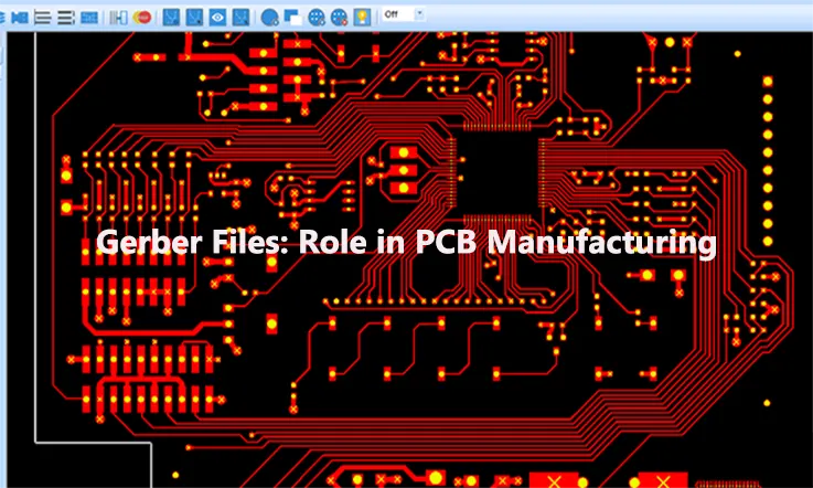
Gerber files play a vital role in translating PCB designs into physical circuit boards. These open ASCII files contain vector data defining each layer of the board layout. Objects like traces, vias, pads, solder masks, and silkscreens are represented through flash and draw codes with associated coordinate points. PCB manufacturers rely on the comprehensive fabrication and assembly instructions provided within Gerber files to produce completed boards.
While generation steps vary across CAD platforms, Gerber files are typically output directly from PCB design software. Most modern Gerber files adhere to the RS-274X standard rather than outdated formats like RS-274-D. As plaintext files, Gerber data has no required filename convention but .GB or .GBR extensions are common.
The extensive layer-by-layer graphical information encoded within Gerber outputs enables manufacturing facilities to accurately transform designers’ intents into functional printed circuit boards. The universality of the Gerber format, combined with over 50 years of industry adoption, solidifies its ongoing importance as a vital data bridge between PCB design and production.
Gerber files are typically generated by PCB design software. Each aspect of the PCB design (such as the layout of copper traces, placement of components, holes, etc.) is represented in a separate Gerber file.
How to Make Gerber File in PCB Design?
Here are the main steps to make a Gerber file in PCB Design:
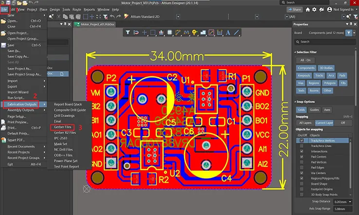
1. Design the PCB in your EDA (electronic design automation) software like Altium, Eagle, KiCad etc. Make sure all the traces, pads, vias, silkscreen layers are designed as per your requirements.
2. Once the PCB layout is complete, go to File -> Plot or Cam Processor. This will open the dialog box to generate manufacturing/Gerber files.
3. Select the layers you want to output – this includes copper layers, solder mask, silkscreen, drill files etc. Make sure to select the appropriate options for each layer like polarity, format etc.
4. Specify the output directory where the Gerber files will be exported.
5. Set the appropriate file extensions for each layer. Common extensions are:
● .GTL – Top Layer
● .GBL – Bottom Layer
● .GTO – Top Solder Mask
● .GBO – Bottom Solder Mask
● .GTP and .GBP – Top and Bottom Paste Layers
● .TXT – Drill File
● .GKO – Outline Layer
6. Configure any other settings like coordinate format, units etc and click on Plot or Generate to create the Gerber files.
7. Carefully review all the generated files to make sure they are correct as per your design. Check file extensions, polarity, alignment etc.
8. Zip the Gerber files and send it to your PCB manufacturer for fabrication. Also send the drill, position and assembly files if needed.
How Gerber Files Are Used In PCB Manufacturing
Gerber files have evolved in tandem with advances in PCB fabrication technology over the decades. Originally, vector photoplotters using apertured light exposure were utilized to image films for board production. Designers worked within the constraints of a limited aperture set. These manual vector plotters have since been replaced by faster raster laser imaging systems.
Gerber’s origins trace back to supplying vector plotters with configuration data, coordinates, aperture selections and flash/draw commands. While laser plotters now convert Gerber files into raster images to guide fabrication, the core data remains compatible. The files’ functionality has expanded to include more settings and definitions, removing previous aperture restrictions.
For example, aperture shapes and dimensions define trace widths and pad sizes, while draw commands determine if lines, fills or flashes are generated. This facilitates flexible, high-precision PCB imaging. Currently, direct laser patterning of copper layers is also emerging to bypass film imaging altogether.
Despite new formats with more intelligence like net connectivity, Gerber files persist as the industry standard. Their simple imaging concept continues suiting PCB production needs. However, measured format evolution does occur to improve manufacturing precision and efficiency. In summary, while fabrication methods advance, Gerber’s fundamental role in conveying PCB design intent to production remains unchanged. Their importance is likely to endure given decades of mass adoption.
Gerber Files: Role in PCB Manufacturing
Gerber files play a vital role in the manufacturing of Printed Circuit Boards (PCBs). They serve as the blueprints for the PCB production process, providing comprehensive information about the board’s design, including copper layers, solder mask, silkscreen, and drill data.
The Role of Gerber Files in Printed Circuit Board (PCB) Manufacturing:
The role of Gerber files in PCB manufacturing is to act as a bridge between the PCB designer and the manufacturer. They are essential in conveying the PCB design accurately and in a universally accepted format.
Ensuring Design Accuracy
Gerber files translate the PCB design into a visual representation that can be read by machines. They ensure that the manufacturer can accurately reproduce the designer’s intent, minimizing the risk of errors and misinterpretations.
Layer-by-Layer Representation
Each layer of the PCB – including copper layers, solder mask, silkscreen, and any other layers – is represented in a separate Gerber file. This layer-by-layer representation allows the manufacturer to produce each layer of the PCB separately before stacking and bonding them together.
Drill Data
Gerber files also provide the drill data, indicating where holes should be drilled in the PCB. These holes are used for mounting components or for vias that connect different layers of the PCB.
Quality Assurance
Manufacturers use Gerber files for quality assurance as well. Comparing the finished product with the original Gerber files can help identify any discrepancies or manufacturing defects.
Benefits of Using Gerber Files
Here are some of the key benefits of using Gerber files in PCB manufacturing:
● Industry Standard – Gerber is the de facto standard format for PCB fabrication data exchange. It is universally accepted by PCB manufacturers.
● Contains All Fabrication Data – The Gerber files contain copper layers, solder mask, silkscreen graphics, board outline etc. All the data needed to physically manufacture the PCB is present in the Gerber set.
● Vendor Independence – Since Gerber is a standard format, it allows taking the design files from one EDA tool and sending it to any PCB vendor for fabrication. No proprietary formats involved.
● Accuracy – The Gerber format provides excellent accuracy in transferring PCB design intent. The files can represent tracks of even a few microns easily. This ensures the fabricated PCB matches the design closely.
● Reliability – Gerber files clearly define the PCB images in a reliable format that has been tried and tested over decades of use. The strict RS-274X standard ensures consistent, error-free results.
● Design Data Exchange – Gerber allows easy exchange of design data between different EDA, CAD and CAM tools through import and export of the standard files.
● Panelization Support – Panelized designs with multiple PCBs can also be streamlined through the Gerber format.
● Established Workflows – Since Gerber format has been used for so long in PCB industry, it integrates seamlessly with established PCB design and manufacturing workflows.
Limitations of Gerber Files
Here are some of the main limitations or disadvantages of using Gerber files in PCB manufacturing:
● File Size – Gerber files can be quite large in size for complex PCB designs as each layer is represented by a separate image file. This increases storage requirements.
● Prone to Errors – Generating accurate and error-free Gerber files requires care. Even simple mistakes like wrong polarity, improper extensions or missing layers can lead to fabrication errors.
● No Intelligence – Gerber files are just images without any intelligence associated with them. So any data about components, nets, etc. is lost.
● Outdated Standards – Some of the Gerber standards are outdated and lack support for modern features like curved tracks, embedded components etc. Updating them is slow.
● Single Image Per Layer – Since each layer has a single image file, it is not possible to have different images on one PCB layer.
● Limited Design Rule Checks – Only basic DRCs related to overlaps and spacing are possible on Gerber files. Advanced DRCs need additional intelligent data.
● Text and Vector Limitations – Rendering etched text and vector lines can be challenging in Gerbers as they are raster images. The outputs may not look smooth.
● No Component Data – No information about components like footprints, pinouts etc. is available. This data needs to be handled separately.
● Panelization Limitations – Basic panelization is possible but advanced panelization features are lacking.
● No Netlist or BOM – Gerber format does not allow inclusion of netlist or bill of materials. These have to be shared separately.
So in summary, Gerber format has some limitations for today’s complex PCB requirements, but it still remains ubiquitous due to its simplicity and wide acceptance.
Conclusion
Gerber files play a critical role in PCB manufacturing by ensuring that the PCB design is accurately translated into a physical product. They provide a comprehensive, layer-by-layer representation of the PCB design, including copper layers, solder mask, silkscreen, and drill data. Without Gerber files, the manufacturing of complex, multi-layer PCBs would be prone to errors and misinterpretation.
Related Posts:
1. Gerber Files: How to Generate in PCB Design Process?
3. ODB++: The Ultimate FAQ Guide in 2023
4. Critical Information about Gerber Files for PCB Manufacturing
5. PCB Bill of Materials: A Comprehensive Guide to Effective Documentation