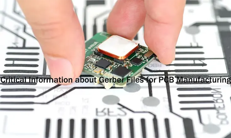
When it comes to fabricating the various elements of your PCB layout, the process involves translating the design data from your CAD system into instructions that manufacturers can follow. To achieve this, you need to generate output files in a suitable format. Among the available options, the Gerber file format is widely used and preferred for most projects. Alternatively, you may also encounter formats such as ODB++ and IPC-2581.
So, what exactly is a Gerber file, and what purpose does it serve in the manufacturing process? In essence, a Gerber file is a standardized format that communicates the necessary information about the PCB design. It contains data regarding the pads, traces, and other relevant elements in both graphical and textual formats. This data is crucial for the fabrication process, as it provides precise instructions to the manufacturer.
Definition of a Gerber File
The Gerber file is a fundamental component of PCB design, deriving its name from Gerber Systems Corp, the pioneering company behind its development. It encompasses various features of the PCB, including solder mask layers, legends, drill templates, and more.
In the process of designing a PCB, CAD systems are commonly utilized, employing manufacturing information to generate two or three-dimensional circuit board designs. However, it is important to note that entering data into these systems is not a straightforward process of automatic design creation. Designers must diligently adhere to the guidelines defined by Gerber files while inputting the necessary information. These files play a crucial role in establishing the requirements at every stage of product development. Notably, Gerber files find utility in both circuit board fabrication and assembly processes.
So what is exactly PCB Gerber files?
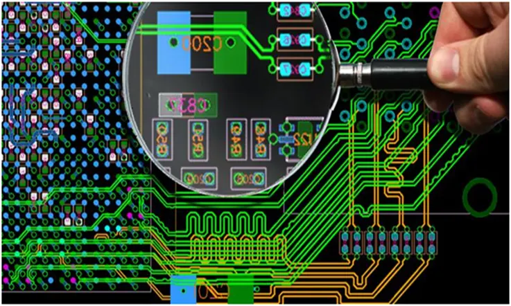
A Gerber file, used in Printed Circuit Board (PCB) design, is an open ASCII vector format file that encapsulates comprehensive information about all the physical layers of a PCB design. This includes details about circuit board copper traces, pads, vias, silkscreen, and solder mask images, all of which are represented by a draw or flash code. These objects are defined through various vector coordinates. In essence, the Gerber file serves as a pivotal tool for PCB manufacturers, enabling them to convert design specifics into tangible attributes of the circuit board.
This underscores the necessity for PCB engineers or designers to ensure the accuracy and comprehensibility of all design details in their Gerber files, in compliance with established standards. Typically, Gerber files are generated by PCB design software suites, although the generation process may vary depending on the CAD tool used. The RS-274X file format (Gerber file) is currently the most widely used format for the creation of bare PCB design files, superseding outdated formats such as the R-274-D Gerber format. Gerber data may use file extensions like .gbr or .gb when presented in a text file, negating the need to assign a unique file name.
How to Make PCB Gerber Files?
Here’s a general process for generating Gerber files from your PCB design. Note that the exact steps may vary depending on the specific software you’re using.
For this guide, I’ll use Eagle, a popular PCB design software:
Complete your PCB design: Ensure your schematic and board layout are complete and fully checked for errors.
Open your PCB design in Eagle: Launch Eagle and open your PCB design.
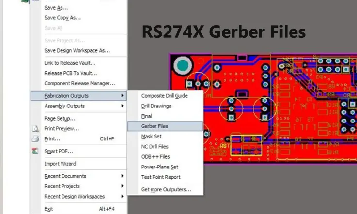
Open the CAM processor: Go to the `File` menu, then select `CAM Processor`. This is the tool that generates the Gerber files.
Configure the CAM processor: You’ll need to tell the CAM processor which layers of your design to include in each Gerber file. Here’s a typical configuration for a two-layer board:
● Top Copper (Gerber file .GTL): Layers 1 (Top), 1-7 (Pads), and 1-8 (Vias)
● Bottom Copper (Gerber file .GBL): Layers 1-6 (Bottom), 1-7 (Pads), and 1-8 (Vias)
● Top Soldermask (Gerber file .GTS): Layer 2-9 (tStop)
● Bottom Soldermask (Gerber file .GBS): Layer 3-0 (bStop)
● Top Silkscreen (Gerber file .GTO): Layers 2-1 (tPlace) and 2-5 (tNames)
● Bottom Silkscreen (Gerber file .GBO): Layers 2-2 (bPlace) and 2-6 (bNames)
● Board Outline (Gerber file .GKO or .GM1): Layer 2-0 (Dimension)
You may need to create a new job for each Gerber file or use a predefined job if one is available that meets your needs.
Generate the Gerber files: Click `Process Job` or a similar command. The CAM processor should generate the Gerber files and save them in the specified location.
Generate a drill file: In addition to the Gerber files, you will also need to generate a drill file (Excellon format). This is often done in the CAM processor as well, using something like the `Drills` or `Holes` tab.
Inspect the Gerber files: Use a Gerber viewer tool to inspect the Gerber files and ensure they represent your design correctly.
Zip the files: Finally, put all the Gerber files and the drill file into a single .zip file. This is the file you will send to the PCB manufacturer.
Remember to check with your specific PCB manufacturer for any special instructions or requirements they may have. They may require certain layers that aren’t included here, or they might want a specific naming convention for the files.
What Should Include In Gerber Files?
When generating gerber files for PCB manufacturing, it is important to include the necessary information across the appropriate layers:
●Enable all signal layers containing traces and routed connections to produce individual gerber files. This provides the manufacturer with the circuit routing information.
●Likewise, enable all power plane layers as separate gerber files. These solid copper pours distribute power across the board.
●The board outline layer should be enabled to convey the physical board edges and dimensions. This keeps components and routing within the required boundaries.
●Any mechanical or non-electrical layers used for assembly or mounting should also have corresponding gerber files. These communicate mechanical details like component placements, mounting hole locations, etc.
●The top and bottom silkscreen overlay layers contain vital nomenclature information such as reference designators, polarity markings, etc. These should be included.
●Prior to generating the gerber set, include overall board dimensions and other vital measurements on the appropriate layer. This facilitates manufacturing.
●Additionally, document the layer stackup by including material details like base thickness, prepreg type, etc. on a mechanical layer. This provides the material construction information.
●Timestamping the individual gerber files assists version control and traceability.
●Carefully validate the gerber set using CAM software to ensure accuracy before releasing to the manufacturer.
Once the comprehensive gerber package has been thoroughly validated, it can be confidently transferred to the manufacturer for procurement.
Gerber File Formats
RS274-D: the earliest Gerber file format developed by Gerber Scientific, was designed as a numerical control (NC) format compatible with various photo plotters prevalent in the 1970s. While it served its purpose during that era, this format exhibited certain limitations, such as the need for manual input of d-codes and user interpretation. Consequently, alternative Gerber file formats were subsequently developed to address these drawbacks. One such format, known as the Standard Gerber, emerged as a successor to RS274-D.
RS274X: Since its introduction in 1998, the RS274X Gerber file format has gained prominence as an improved version of RS274-D. This revised format incorporates embedded formatting, unit, and data information. Notably, it allows for the embedding of apertures that define the layers, facilitating the utilization of both standard sizes and customized apertures. Furthermore, RS274X offers a range of enhanced features for designers, such as film control, support for multiple layer structures within a single layer, specialized polygon fill commands, polarity controls, and various other capabilities. By eliminating the need for manual data entry and significantly reducing photo plotting errors, this improved format has become exceptionally reliable and error occurrences have become exceptionally rare.
ODB++: is an all-inclusive and standardized input format developed by Valor with the objective of streamlining the design process. It functions as a self-extracting format, automating tasks such as stackup definition, drill placement, and labeling. Initially, compatibility with other software programs was limited, but nowadays, most CAD programs can accept ODB++ files as input. By eliminating the need for manual naming conventions and minimizing the potential for human error, ODB++ encapsulates all design and fabrication information, along with netlist data, within a single compressed file. While it may not be the preferred format for everyone, it has gained significant utility within the industry.
Gerber X2: represents the latest iteration of the Gerber format and is specifically designed to cater to advanced CAM (Computer-Aided Manufacturing) software applications. It introduces the capability to assign attributes to specific features within the Gerber file, which can then be interpreted and implemented by the CAM software. This additional information benefits both the fabricator and the CAM operator. Examples of attributes that can be applied within the Gerber file include specifying the function of a file (e.g., top mask, top copper), indicating the part represented by the file (e.g., single PCB, array, coupon), and defining the function of a pad (e.g., SMD, via pad, fiducial). Gerber X2 maintains compatibility with its predecessor, the X1 format, enabling designers to transfer valuable design information seamlessly to the Gerber format.
Application of the Gerber File in PCB Fabrication
The historical background of PCB technologies holds significant importance when considering the application of Gerber files in PCB manufacturing. In earlier times, vector photo-plotters played a dominant role in producing PCB tooling films for the manufacturing process. These plotters utilized focused light, directed through apertures, to expose the film, thereby creating individual traces and pads.
This historical perspective is crucial for comprehending how the evolution of technology and equipment in PCB manufacturing has greatly influenced the utilization of Gerber files. With advancements in technology, the application of Gerber files has undergone notable transformations. For instance, the limited availability of aperture sets in earlier manufacturing methods compelled designers to employ creative strategies, particularly in constraining their lines and flashes based on the resources at their disposal.
By understanding this historical context, we gain deeper insights into the challenges and limitations that designers faced in the past, which subsequently shaped the development and usage of Gerber files. The progressive advancements in PCB manufacturing technology and equipment necessitated the emergence of more sophisticated file formats like Gerber, capable of accommodating the demands of modern manufacturing processes and supporting the growing intricacies of PCB designs.
Application
The Gerber file plays a pivotal role in PCB fabrication, serving as the standard file format utilized to communicate PCB design information between designers and manufacturers. It contains the necessary data and instructions to guide the fabrication process accurately. Here are some key aspects of the Gerber file’s application in PCB fabrication:
PCB Layer Information: The Gerber file provides detailed information about each layer of the PCB, including the top copper, bottom copper, solder mask, silkscreen, and other relevant layers. Each layer is represented as a separate Gerber file, allowing manufacturers to understand the specific design requirements for each layer.
Traces and Pads: The Gerber file defines the shape, size, and position of traces, pads, and vias on the PCB. It specifies the widths, clearances, and other design parameters, ensuring that the fabrication process accurately reproduces the desired electrical connections and component placements.
Aperture Definitions: Gerber files include aperture definitions that specify the shapes and dimensions of different features, such as pads, lines, arcs, and polygons. These definitions control the size and shape of the various elements on the PCB and provide instructions for their fabrication.
Drill and Hole Information: Gerber files also contain information about drill holes, including their positions, sizes, and types (such as plated or non-plated). This data guides the drilling process, ensuring accurate hole placement and dimensioning.
Manufacturing Instructions: Along with graphical data, Gerber files may include additional information such as component identifiers, reference designators, and assembly instructions. These instructions aid in the PCB assembly process and help manufacturers correctly populate and solder components onto the board.
Design Verification: PCB manufacturers use Gerber files to verify the design integrity before fabrication. They can analyze the Gerber data using specialized software or Gerber viewers to detect errors, such as missing or overlapping features, and ensure the design meets the required specifications.
Compatibility and Standardization: The Gerber file format has become an industry-standard for PCB fabrication, ensuring compatibility across different software tools and manufacturing processes. It enables seamless communication between designers and manufacturers, streamlining the fabrication workflow.

All in all, the Gerber file is instrumental in PCB fabrication, providing essential information about PCB layers, traces, pads, apertures, drills, and manufacturing instructions. It facilitates accurate reproduction of the PCB design, ensures compatibility, and acts as a bridge between design and manufacturing processes.
Summary
The Gerber file format serves as the de facto standard for facilitating communication between PCB design engineers and manufacturers. Specifically, it adopts the RS-274-X 2D ASCII file format, encompassing comprehensive information pertaining to conductive, mechanical, textual, and keepout layers of a PCB design, along with essential manufacturing notes.
Utilizing the RS-274-X format entails generating a distinct file for each layer of the PCB, a practice widely favored within the PCB industry. It is crucial for designers to exercise meticulous care when incorporating layers to ensure the accurate generation of these files. Any uncertainties or incorrect data in this process may result in an unexpected and undesirable PCB outcome, rendering it essentially useless or substandard.
Related Posts:
1. Gerber Files: How to Generate in PCB Design Process?
2. Gerber Files: Role in PCB Manufacturing
3. ODB++: The Ultimate FAQ Guide in 2023
5. PCB Bill of Materials: A Comprehensive Guide to Effective Documentation