Printed circuit boards (PCBs) form the operational platforms for nearly all modern electronic devices. Among the substrate materials used in their construction, fiberglass composites, especially FR-4, are widely employed. This leads to fundamental questions: What precisely defines a Fiberglass PCB, and what attributes account for its extensive application in PCB Manufacturing?
This document addresses these inquiries through a detailed exploration of Fiberglass PCB technology. We will examine Fiberglass PCB materials, including FR-4 and its properties, and categorize the various Fiberglass PCB types. The discussion will cover Fiberglass PCB design considerations, the intricacies of the Fiberglass PCB manufacturing lifecycle—from fabrication to assembly and finishing—and aspects of quality assurance and reliability.
Defining Fiberglass PCB: The Foundational Substrate
Fiberglass PCBs form the workhorse platform for countless electronic devices. Understanding their core, especially the widely used FR-4 material, is the first step towards successful product development. This section explores not just what these materials are, but how their properties influence design and, directly, how we leverage them in our manufacturing and assembly services to benefit your project.
Unveiling Fiberglass PCB Materials: The Core Composition
Consider a Fiberglass PCB as a precisely structured composite, not merely a single element. It is a blend where different materials unite, each contributing to the creation of a sturdy, dependable base for electronic components. Appreciating this structure helps in understanding how these boards operate and how our processes ensure their integrity.
●What is Fiberglass PCB?: Uncovering the Basics?
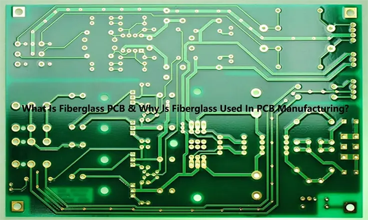
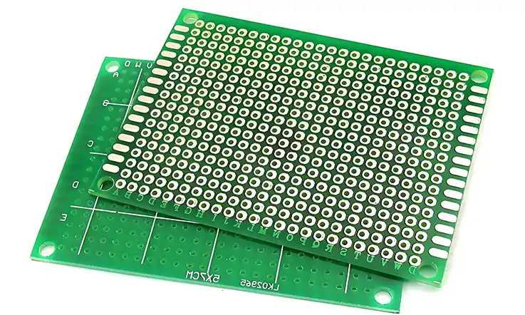
A Fiberglass PCB is a circuit board where the insulating base is constructed from sheets of Woven Fiberglass fabric thoroughly impregnated with an Epoxy Resin binder. This Glass Fiber PCB material provides both structural support and electrical isolation. It forms the surface upon which conductive copper pathways are etched. Its favorable combination of mechanical strength, electrical performance, and manufacturing cost makes it a standard selection for a vast range of electronic applications – a combination that we expertly handle in our production.
●Glass Fiber PCB, Woven Fiberglass & Epoxy Resin PCB Explained
The “Woven Fiberglass” component is a fabric-like material, providing strength and dimensional stability. This fabric is infused with an “Epoxy Resin,” a thermosetting polymer that hardens upon curing, acting as a binder and insulator. This process creates a solid Epoxy Resin PCB. When fiberglass provides the reinforcement, Glass Fiber PCB or Glass Epoxy PCB are the specific descriptors for these widely manufactured boards.
Introducing FR-4: The Industry Standard Fiberglass PCB Material
FR-4 is the most widely recognized material within the Fiberglass PCB landscape. You will frequently encounter it. Its widespread use stems from its practical, well-rounded set of capabilities that meets broad industry needs – needs that we have addressed for countless clients over many years.
●Understanding FR-4 Material & FR-4 Glass Epoxy
FR-4 Material signifies “Flame Retardant 4”. The “FR” indicates its self-extinguishing characteristic, a safety feature. The “4” represents a grade defined by NEMA. It is a specific type of FR-4 Glass Epoxy, utilizing woven glass and an epoxy system formulated to meet fire safety standards. It provides solid strength with manageable weight and reliable electrical insulation.
●Why FR-4 is the Preferred PCB Substrate Explained?
Why is FR-4 so common? The PCB Substrate Explained simply: it offers an advantageous cost-to-performance ratio. It provides dependable electrical separation, handles heat adequately for numerous applications, possesses good physical strength, and its well-established manufacturing processes make it reasonably priced. This combination makes it a frequently selected PCB substrate, and its familiarity allows our production lines to operate with high efficiency, translating into reliable delivery and cost advantages for your projects.
Key Fiberglass PCB Materials Properties: Performance Deep Dive
Understanding its composition leads to appreciating its performance. These FR-4 Material Properties directly influence circuit behavior and manufacturability. This is where material science meets practical application – and where our expertise adds value.
●Electrical Properties: PCB Insulation & Dielectric Constant
Electrically, FR-4 functions as an effective insulator – its PCB Insulation qualities prevent current from flowing in unintended paths. Design specialists closely monitor the Dielectric Constant (Dk), as this value affects signal propagation speed and impedance control. While FR-4’s Dk offers a degree of predictability, managing its variations with frequency requires careful consideration during high-speed design – a challenge our team can help you navigate.
●Mechanical Properties: High Strength, Durability & Dimensional Stability
These boards possess considerable physical resilience. They exhibit High Strength PCB features, resisting bending and impacts. This Durability means boards built by our expert assembly teams can withstand handling and operational demands. Furthermore, their Dimensional Stability ensures they maintain their form across temperature variations, contributing to a longer product lifespan and reliable device operation.
●Thermal Properties & Flame Retardant PCB Safety
Standard FR-4 manages typical operational temperatures and soldering without issue for many devices. While not designed for extreme high-temperature environments, it is sufficient for many uses. Its Flame Retardant PCB Safety (typically meeting UL 94V-0) is a pronounced benefit, contributing to product safety across many industries – a compliance aspect we ensure in our certified processes.
Exploring Fiberglass PCB Types: A Comprehensive Overview
Fiberglass PCBs offer a spectrum of solutions, moving beyond a single, uniform approach. Different electronic applications present unique demands, which are met by a diverse range of board configurations. Understanding these Fiberglass PCB types is a foundational step in selecting an appropriate platform for any electronic project to meet its performance requirements. This section outlines the different categories to provide clarity on the available options.
Classifying Fiberglass PCB Types by Layer Count
A primary method for categorizing these boards involves their number of conductive copper layers. This count directly corresponds to the complexity of the circuits they can accommodate. An increased number of layers provides greater space for routing, facilitating more compact and intricate designs.
| PCB Type | Layers | Cost | Design Complexity | Common Applications |
| Single-Sided | 1 | Low | Low | Toys, power supplies, simple gadgets |
| Double-Sided | 2 | Moderate | Moderate | Consumer electronics, control systems |
| Multi-Layer (4+) | 4 – 40+ | High | High | Servers, medical devices, telecom systems |
●Single-Sided PCB / Single Layer PCB: Simple & Cost-Effective
The most fundamental form is the Single-Sided PCB or Single Layer PCB. It features copper pathways on only one side of the substrate. These boards are generally inexpensive to produce and straightforward to design, frequently found in applications with lower complexity where cost considerations are a large factor. They provide a functional solution for basic electronic tasks.
●Double-Sided PCB / Double Layer PCB: Versatility & Density
For increased capability, the Double-Sided PCB or Double Layer PCB presents a solution. Featuring copper on both sides interconnected by vias (plated-through holes), this type offers significantly more area for routing traces and placing components. This enhanced density and versatility make them suitable for a wide spectrum of electronic devices.
●Multi-Layer PCB: For Complex & High-Performance Designs
For advanced applications, the Multi-Layer PCB is utilized. These boards integrate multiple double-sided layers, bonded together, creating a three-dimensional structure for highly complex circuits. With four or substantially more layers, these boards support demanding high-performance designs, such as those in servers, advanced telecommunications equipment, or medical technology, allowing for high functionality within a limited area.
Understanding Fiberglass PCB Types by Rigidity & Structure
Beyond layer count, the physical characteristics, specifically rigidity, define another set of board categories. While the majority are rigid, certain applications necessitate flexibility or a combination of rigid and flexible sections, leading to different structural approaches.
| Structure Type | Rigidity | Typical Substrate | Common Uses | Cost |
| Rigid PCB | Rigid | FR-4 | Computers, consumer electronics | Low to Moderate |
| Flexible PCB | Flexible | Polyimide | Wearables, foldable phones, sensors | Moderate to High |
| Rigid-Flex PCB | Rigid + Flexible | FR-4 + Polyimide | Aerospace, medical implants, military tech | High |
●Rigid Fiberglass PCB & Rigid Circuit Board Construction
The most common form is the Rigid Fiberglass PCB. It is stiff and provides a stable platform for components. The Rigid Circuit Board Construction, typically using standard FR-4, represents the majority of boards manufactured and serves as the standard, reliable choice for applications where the board remains stationary.
●Exploring Flexible & Rigid-Flex PCB Possibilities
Certain applications require creative structural solutions. Flexible & Rigid-Flex PCB Possibilities allow circuits to be installed in confined spaces, connect parts that move relative to each other, or form three-dimensional assemblies. While flexible circuits often use polyimide, rigid-flex designs frequently combine FR-4 sections with flexible interconnects, offering a blend of stability and bendability, usually at a different cost point.
●High-Density Interconnect (HDI) as Advanced Fiberglass PCB Types
High-Density Interconnect (HDI) boards represent Advanced Fiberglass PCB Types. These utilize fabrication techniques such as microvias, very fine lines and spaces, and sequential lamination to achieve exceptionally high circuit density. They are a requirement for miniaturized modern devices and signify a progression in technology.
Specialized Fiberglass PCB Types: Meeting Niche Demands
Standard configurations are not always sufficient. Specific applications present unique challenges that necessitate specialized board designs, often based on fiberglass principles but modified for particular performance characteristics.
| Specialized PCB Type | Focus Area | Material Basis | Key Benefit | Application Fields |
| High-Frequency PCB | RF / Microwave Signals | Advanced FR-4 / Rogers | Low dielectric loss, signal integrity | Antennas, radar, satellite communication |
| Heavy Copper PCB | Power & Thermal | Thick Copper on FR-4 | High current & heat handling | Automotive, power electronics |
| Alternative Materials | Special Environments | Varying fiberglass blends | Tailored mechanical or thermal characteristics | Aerospace, oil & gas |
●High-Frequency PCB: Utilizing FR-4 Effectively
Applications involving radio frequencies or high-speed digital signals present a distinct set of challenges. A High-Frequency PCB requires materials with specific dielectric properties (low Dk and Df). While specialized substrates are available, careful Fiberglass PCB design and the use of certain advanced FR-4 grades can be an effective approach, especially when managing production costs.
●Heavy Copper PCBs: Power & Thermal Types
When managing substantial electrical currents or dissipating significant amounts of heat is necessary, Heavy Copper PCBs are employed. These boards are enhanced with thicker copper layers on an FR-4 base. These Power & Thermal Types are used in power conversion, motor control, and automotive systems where standard boards would not suffice.
●An Introduction to Alternative Fiberglass PCB Types
While FR-4 is prevalent, it is useful to have an Introduction to Alternative Fiberglass PCB Types. Other fiberglass-based composites exist, offering variations in thermal performance or mechanical strength. These alternatives provide designers with additional options to configure a board precisely for its intended operational environment.
The ‘Why’ Behind It: Fiberglass in PCB Manufacturing
After examining the composition and varieties of these circuit boards, a central question surfaces: What makes fiberglass the prevalent choice? Given the array of available materials, the widespread preference for this glass-epoxy composite in Fiberglass PCB manufacturing warrants exploration. Its extensive use is not a matter of chance but is rooted in discernible, functional attributes. This segment delves into these attributes, clarifying the real-world advantages and the way this material’s characteristics facilitate the creation of dependable electronic assemblies that are integral to modern life.
Fiberglass PCB Manufacturing: The Advantages Unpacked
When design specialists and production supervisors assess substrate options, fiberglass often stands out as a highly suitable selection. It offers a suite of beneficial properties that are compelling, contributing to streamlined production workflows and the realization of high-caliber end-products. Its use facilitates the achievement of dependable outcomes via established fabrication techniques.
●Key Benefits of Fiberglass PCB: Strength, Insulation, Cost-Effectiveness
This substrate material provides a compelling union of three distinct merits. Firstly, its Strength: the interwoven glass filaments impart considerable physical resilience, enabling the board to withstand mechanical stresses without fracturing or deforming. Secondly, its Insulation: the epoxy binder forms an effective dielectric barrier, directing electrical current flow along intended paths and preventing unintended shorts. Thirdly, its Cost-Effectiveness: the level of performance it offers is achievable at a production expenditure that aligns with broad market requirements, making the Advantages of Fiberglass PCB persuasive for a multitude of projects.
●Why It’s the Go-To Choice for Electronics Manufacturing
This collection of traits clarifies Why It’s the Go-To Choice for Electronics Manufacturing. Professionals throughout the industry appreciate its adaptability in processing – it can be drilled, machined, and soldered with predictable results. Product developers benefit from its well-documented performance envelope. For a Fiberglass PCB manufacturer, the capacity to generate large quantities with reliable outcomes underpins a responsive supply chain. Its frequent selection is thus founded on these substantial merits.
●Comparing Fiberglass vs. Other Materials in PCB Manufacturing
While other substrate materials are available, Comparing Fiberglass vs. Other Materials frequently underscores its well-rounded characteristics. Some alternatives might present lower initial material costs but may not offer comparable mechanical robustness. Others could yield superior thermal conduction but involve increased expenditure and more complex processing. FR-4 commonly provides a versatile foundation, satisfying a wide array of needs within PCB Manufacturing. For applications with extreme high-frequency or thermal demands, alternative substrates may be explored, and material specialists can provide guidance on FR-4’s suitability or the selection of alternatives like Rogers materials or metal-core PCBs.
How Fiberglass Enhances PCB Reliability and Durability?
Initial functionality upon assembly is one aspect of performance; sustained operation throughout a device’s expected service duration, often under diverse conditions, is another. Fiberglass makes a substantial contribution to a circuit board’s capacity to endure operational challenges, leading to more robust and dependable electronic products.
●Ensuring PCB Reliability through Material Choice
The pursuit of PCB Reliability is fundamentally linked to the selection of the base substrate. Fiberglass furnishes a stable structural base that resists dimensional changes, fractures, or degradation under typical operational parameters. Its comparatively low moisture uptake, relative to some other dielectrics, helps preserve stable electrical characteristics over time, which supports predictable device operation. Controlled manufacturing environments further ensure this stability translates directly into trustworthy device performance.
●Mechanical Support PCB & Resistance to Physical Stress
Functioning as a Mechanical Support PCB, fiberglass demonstrates commendable performance. It provides the necessary rigidity to securely hold electronic components, including those of greater mass. It offers effective Resistance to Physical Stress, such as shocks encountered during product handling or vibrations experienced in operational settings, thereby protecting the delicate copper conductive patterns. Circuit boards are often structured to endure these common real-world forces.
●Long-Term Performance in Various Environments
These circuit board structures are developed for enduring service. The cured epoxy resin component exhibits resistance to a wide array of common chemicals. They preserve their structural integrity and electrical behavior across a functional temperature spectrum, facilitating Long-Term Performance in varied settings, from controlled office atmospheres to more demanding industrial locations. Protective measures like conformal coating, a service offered by fabricators, can further enhance this durability in specific challenging environments.
The Manufacturing Process: Leveraging Fiberglass Properties
The practical utility of fiberglass is also evident in its compatibility with established manufacturing workflows. Its inherent physical and chemical nature aligns well with the precise and often intricate steps involved in transforming a digital circuit design into a tangible physical object.
●How Fiberglass PCB is Made: An Overview
A review of How Fiberglass PCB is Made underscores its process adaptability. The sequence typically commences with Copper Clad Laminate (CCL) panels. These panels undergo imaging to define the circuit, etching to remove unwanted copper, drilling for vias and component mounting, plating to create conductive interconnections, and lamination to bond multiple layers in multi-layer constructions. The dimensional stability of the fiberglass base throughout these operations allows for the high degree of precision needed for fine-featured patterns, a level of exactitude that modern automated equipment reliably achieves in proficient facilities.
●The PCB Lamination Process & Copper Clad Laminate (CCL)
In the fabrication of multi-layer circuit boards, The PCB Lamination Process serves to fuse the individual layers into a cohesive structure. Sheets of etched inner-layer Copper Clad Laminate (CCL) are carefully arranged with layers of ‘prepreg’ (fiberglass cloth partially saturated with epoxy resin). This assembly is then subjected to carefully controlled cycles of heat and pressure, causing the prepreg to liquefy, flow, and cure, thus bonding the stack. The inherent properties of fiberglass facilitate the precise alignment required during this demanding stage, a process managed with exacting control using multi-stage presses and often verified with automated optical systems in well-equipped plants.
●Etching Process PCB & Circuit Formation
The Etching Process PCB is a selective copper removal technique used to define the conductive pathways. A patterned protective layer shields the desired copper circuitry while a chemical solution dissolves the exposed, unwanted copper. Meticulous control over this step ensures the formation of sharply defined conductive tracks and pads. Achieving accurate results at this juncture enables the intended electrical functionality of the circuit, an outcome delivered with high yield by advanced chemical lines at proficient manufacturing sites.
Fiberglass PCB Design: Structuring for Success
While familiarity with materials and board configurations provides an initial understanding, the actual creation of functional electronic pathways occurs during the Fiberglass PCB Design phase. This activity extends beyond mere electrical point-to-point connections; it is the art of architecting electronic systems. Those specializing in this field apply their knowledge, navigating the interplay of physical principles, manufacturing limitations, and project aims. A competently developed design operates as intended, can be produced without excessive difficulty, and aligns with fiscal expectations for production. This segment illuminates the elemental aspects of developing these fiberglass-based platforms, and clarifies how collaboration with a seasoned manufacturing entity can help transition a thoughtfully structured design into a high-performing physical circuit board.
Core Principles of Fiberglass PCB Design
Attaining favorable results with intricate designs necessitates a firm grasp of fundamental approaches. These core practices are the underpinnings for developing dependable, manufacturable circuit boards. Observance of these practices from a project’s outset helps avert later complications.
| Design Aspect | Recommended Practice | Benefit |
| Trace Width & Spacing | Follow IPC-2221 standards | Reliable signal and power transmission |
| Via Types | Use appropriately sized and placed vias | Avoids manufacturing defects |
| Component Placement | Maintain sufficient clearance and logical layout | Enhances assembly and minimizes rework |
| Layer Stack Planning | Define early, including ground/power planes | Supports EMI control and power integrity |
●Circuit Board Design Guidelines for FR-4
Application of recognized Circuit Board Design Guidelines for FR-4 is a customary part of product development. These directives outline specifications such as minimum conductor widths and separations, via hole attributes, and component placement clearances. Following such parameters facilitates efficient fabrication processes. Comprehensive guidelines, often refined from considerable manufacturing exposure, assist in preparing FR-4 board layouts for streamlined production from the initial design stages.
●Fiberglass PCB Design: Balancing Performance and Cost
A central consideration in Fiberglass PCB Design involves Balancing Performance and Cost. Technical specialists work to meet operational benchmarks for elements like signal velocity or power distribution capacity, while concurrently managing the overall PCB Cost. Choices related to layer count, trace pathway geometries, and material grades directly influence the final expense of production. Effective development work finds a suitable equilibrium between these elements. Technical teams at manufacturing operations often engage with clients to explore these variables, seeking an advantageous reconciliation of performance objectives and budgetary frameworks.
●PCB Stackup Design & Its Influence
The PCB Stackup Design functions as the internal constructional map for a multi-layered circuit board. It delineates the sequence and properties of copper conductive layers and FR-4 insulating strata (comprising cores and prepregs). This layered arrangement has a pronounced Influence on impedance characteristics, signal transmission quality, electromagnetic compatibility (EMC), the efficacy of power delivery networks, and thermal dissipation. Establishing a thoroughly planned stackup early in the development cycle is a beneficial approach. Expert assistance in PCB stackup design, including support for intricate structures incorporating controlled impedance or varied dielectric materials, is often accessible through proficient manufacturers, enabling a board to realize its designated electrical behavior via precise fabrication.
Advanced Fiberglass PCB Design Considerations
As electronic apparatus increases in operational speed and structural complexity, product developers face more demanding technical hurdles. Employing FR-4 in such contexts necessitates a comprehension of sophisticated techniques and material attributes to achieve the desired operational outcomes.
| Advanced Design Factor | Challenge Addressed | Common Technique | Impact |
| Signal Integrity | High-speed data degradation | Controlled impedance routing | Maintains signal quality |
| EMC/EMI Performance | Electromagnetic interference | Dedicated ground planes, shielding | Ensures regulatory compliance |
| Thermal Dissipation | Heat from power-intensive components | Copper pours, thermal vias | Enhances board reliability |
| Fabrication Complexity | Tight tolerances, fine features | HDI techniques, DFM collaboration | Reduces scrap and improves yield |
●Signal Integrity & High-Speed Design on FR-4
When electrical signals function at elevated frequencies, maintaining Signal Integrity in High-Speed Design on FR-4 requires meticulous planning. The inherent dielectric characteristics of FR-4 can lead to the degradation of signal quality. Many involved in product creation utilize methods such as controlled impedance routing, careful layer assignment for signal paths, and optimized conductor geometries to counteract these effects and preserve clear signal transmission. Manufacturing capabilities that support fine tolerance control for traces and spacing are needed for these designs, and technical support teams can often furnish insights derived from advanced modeling to help verify signal path attributes on FR-4 prior to fabrication.
●PCB Design Tips for Manufacturability (DFM)
Integrating Design for Manufacturability (DFM) strategies during the initial design phase generally contributes to a smoother transition to production and can help manage expenditures. These PCB Design Tips encompass attention to component placement to prevent assembly difficulties, utilization of standard drill bit sizes, provision of clear panelization schemes, and avoidance of features that might unduly complicate production. Thorough DFM reviews, a valuable service offered by manufacturing partners, frequently pinpoint opportunities for optimizing via structures or adjusting solder mask clearances, which can directly enhance manufacturing yields and lessen assembly complications for a Fiberglass PCB.
●Integrating Through-Hole Technology & SMT in Design
Numerous contemporary electronic designs benefit from Integrating Through-Hole Technology (often chosen for connectors or components handling higher power) with Surface Mount Technology (SMT) (selected for achieving high component density). Arranging a Fiberglass PCB to effectively utilize both requires careful forethought regarding the distinct assembly procedures and thermal profiles associated with each technology on a singular board. Assembly lines at proficient facilities are equipped to process mixed-technology boards, ensuring dependable soldering and component placement for both SMT and Through-Hole parts.
Selecting Fiberglass PCB Materials in Design
Even when FR-4 is the chosen category, specific material selections remain. The particular grade of FR-4 designated can noticeably affect board performance, particularly under strenuous operating conditions.
| FR-4 Grade | Glass Transition Temp (TG) | Thermal Stability | Typical Use Cases |
| Standard TG | ~130°C | Basic thermal performance | Consumer products, office electronics |
| Mid TG | ~150°C | Moderate improvement | Automotive electronics, industrial control |
| High TG | 170°C and above | High thermal cycling resistance | Telecom, servers, power devices |
●Choosing the Right FR-4 Grade: Standard, Mid, High TG FR4
Choosing the Right FR-4 Grade is contingent upon the board’s anticipated operational thermal environment. Standard TG FR4 proves adequate for many common uses. However, for boards that will be subjected to higher operational temperatures or considerable thermal cycling, selecting Mid TG FR4 or High TG FR4 offers enhanced thermal resilience. Material specialists can provide guidance in selecting the most fitting FR-4 grade from available inventories, based on an application’s specific thermal and operational characteristics, with the aim of ensuring longevity and performance.
●FR-4 Laminate & Prepreg (PP) Selection
For circuit board construction, it is frequently necessary to designate the specific FR-4 Laminate (the core layers) and Prepreg (PP) (the bonding sheets) to be employed. Different material types present variations in electrical behavior and physical thickness. This Selection is particularly relevant for high-speed or controlled impedance designs where predictable material response is a primary consideration. Well-documented stocks of various FR-4 laminates and prepregs, accompanied by clear specifications, are maintained by diligent suppliers to aid selection for designs that call for precise electrical outcomes.
●Considering FR-4 Properties in Your Design
Diligent preparation yields positive results. Considering FR-4 Properties in Your Design involves assessing its Dielectric Constant, coefficient of thermal expansion, and moisture absorption characteristics. A lucid comprehension of how these attributes align with the circuit’s functional needs helps in foreseeing and averting potential operational difficulties.
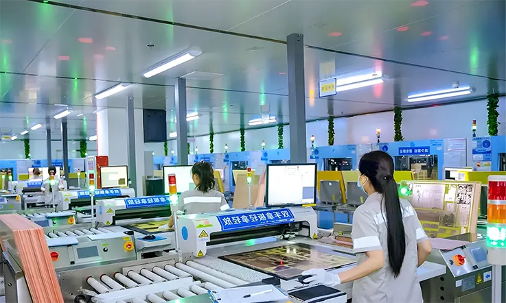
The Fiberglass PCB Manufacturing Lifecycle
Following design and material selection, the process of converting a digital file into a physical Fiberglass PCB commences. This transformation represents the Fiberglass PCB manufacturing lifecycle. It is a journey that utilizes specialized machinery, precise chemical processes, and skilled technicians. It requires a high degree of technological application and attention to detail.
From Design to Reality: PCB Fabrication Process Steps
Fabrication constitutes the stage where the bare board structure and its copper pathways are constructed. This foundational work precedes component placement and necessitates precision throughout every step, ensuring the board performs reliably in its end application.
●Understanding PCB Manufacturing Steps
The PCB Manufacturing Steps adhere to a defined sequence, often governed by IPC standards. The process initiates with cutting the raw, copper-clad FR-4 sheets to the required size and preparing them for imaging. Subsequently, holes are drilled with high accuracy for vias and component mounting, often utilizing CNC drilling machines for optimal placement. A photolithographic process then transfers the circuit pattern onto the board surface. Following this, unwanted copper is chemically removed through etching. For multi-layer boards, the individual layers are then pressed together. This is a detailed procedure.
●The Ins and Outs of the PCB Lamination Process
For multi-layer boards, The PCB Lamination Process is a central operation where the layers are bonded. Etched inner core layers are interleaved with sheets of ‘prepreg’ (fiberglass cloth partly cured with epoxy) and outer copper foils. This stack is then subjected to intense heat and pressure within our multi-stage presses, causing the prepreg to flow and cure, fusing all layers into a monolithic structure. The stability offered by the Fiberglass PCB materials allows for the necessary alignment.
●Key Aspects of the Etching Process PCB
The Etching Process PCB is a subtractive method. A protective layer shields the desired copper pattern while chemical solutions dissolve the exposed, unwanted copper. Precise control over this step ensures the formation of well-defined copper tracks and pads, directly impacting circuit performance. Achieving accurate results here enables the intended circuit functionality.
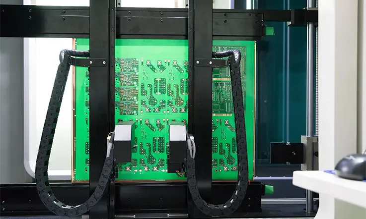
Precision Assembly in Fiberglass PCB Manufacturing
A bare board requires electronic components to perform its function. The assembly stage involves populating the board by placing and soldering resistors, capacitors, integrated circuits, and connectors. This integrates the board’s operational elements with high precision.
●Overview of Fiberglass PCB Assembly Services
As a comprehensive service provider, we offer end-to-end Fiberglass PCB Assembly Services (PCBA). Our process includes automated solder paste application via high-precision stencils with 2D/3D inspection, utilizing advanced pick-and-place machines to position components with high speed and accuracy, and then passing the boards through carefully profiled reflow ovens (for SMT) or wave soldering systems (for through-hole) to establish permanent, reliable electrical connections that meet IPC-A-610 standards.
●Surface Mount Technology (SMT) Assembly
Surface Mount Technology (SMT) Assembly is the predominant method in modern production. Small components are mounted directly onto surface pads. SMT facilitates high component density and automated assembly, making it well-suited for complex devices often built on advanced Fiberglass PCB types. Our state-of-the-art SMT lines handle a diverse range of component packages, from minute 01005 passives to complex BGAs and fine-pitch QFPs, with exceptional placement accuracy and speed, supported by post-reflow Automated Optical Inspection (AOI).
●Traditional Through-Hole Technology Assembly
While SMT is widely used, Traditional Through-Hole Technology Assembly remains relevant. Components with leads are inserted into drilled holes and soldered on the opposite side. This established and reliable method is often employed for components requiring additional mechanical support or those not available in SMT packages. We maintain dedicated through-hole assembly capabilities, including options like selective soldering, to ensure robust and lasting connections for these components on your Fiberglass PCB designs.
Finalizing the Board: Finishes and Coatings
Before a board is considered complete, several finishing steps are performed to protect it and prepare it for its operational lifespan. These applications contribute to the board’s longevity, solderability, and overall usability.
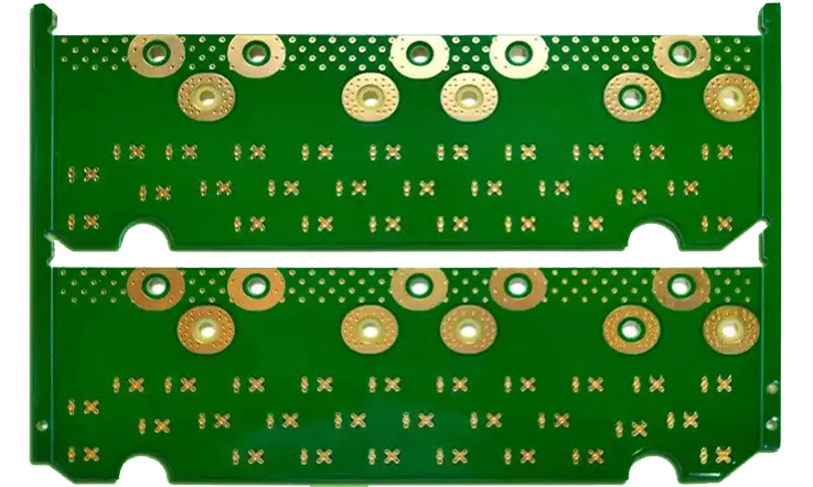
●Solder Mask Application and Its Function
The typically green layer on a PCB is the Solder Mask. Its Solder Mask Application serves a dual purpose. It functions as a protective outer layer, shielding copper traces from oxidation and preventing accidental short circuits during handling and assembly. It also creates defined openings over the solder pads, guiding the soldering process and helping to prevent solder bridges. We offer various solder mask colors (green, blue, red, black, white) and apply Liquid Photoimageable (LPI) solder mask using precision methods to achieve optimal coverage and accurate pad definition.
●Surface Finish Options (HASL, ENIG, etc.)
The exposed copper pads require a protective layer to maintain solderability over time. Several Surface Finish Options are available. Each presents different characteristics regarding cost, shelf life, suitability for fine-pitch components, and RoHS compliance.
●Conformal Coating for Protection
For boards intended for use in challenging environments (e.g., high humidity, dust, chemical exposure, or vibration), an additional layer of Conformal Coating for Protection may be applied. This thin polymer layer provides environmental protection for the entire assembly, shielding it from contaminants.
Cost Factors & Value Engineering with Fiberglass PCBs
Addressing the financial aspects directly is a common practice in electronics development. While creating functional electronic designs is a primary objective, managing production costs remains a parallel consideration. Understanding what influences the PCB Cost facilitates budget management and helps deliver products at accessible price points. This requires a balancing act between technical specifications and financial constraints. Through diligent planning and Value Engineering practices, it is possible to navigate the financial dimension of Fiberglass PCB manufacturing effectively. This section examines cost elements and methodologies for prudent expenditure.
Identifying Key Fiberglass PCB Cost Drivers
Before cost management strategies can be implemented, it is necessary to identify where expenditures occur. Several factors contribute to the final price of a Fiberglass PCB. A clear understanding of these drivers permits informed decision-making during the design and procurement phases.
●How Fiberglass PCB Materials Impact Price?
The selection of Fiberglass PCB Materials directly Impacts Price. Standard FR-4 typically offers a cost-effective base. However, requirements for materials like High TG FR4 (for higher thermal tolerance) or specialized low-loss laminates for high-frequency applications will generally increase material expenses. In some scenarios, a higher upfront material investment can prevent costlier issues later. Material specialists at manufacturing facilities often assist clients in analyzing these trade-offs, advising on materials that meet performance needs without unnecessary expense.
●Design Complexity, Tolerances, and Layer Count
The intricacy of the board structure influences costs. Higher Design Complexity, tighter manufacturing Tolerances, and an increased Layer Count will usually result in higher production costs. Additional layers necessitate more lamination cycles and processing steps. Finer lines, smaller vias, and stricter tolerances often require more advanced fabrication equipment. A manufacturer’s DFM review process often targets areas where design complexity or tight tolerances might escalate costs, offering practical alternatives.
●Volume, Lead Time, and Finishing Options
Production logistics also affect the final price. Larger production Volume orders typically allow for lower per-unit costs due to economies of scale. Requests for expedited production (short Lead Time), often termed Quick Turn PCB services, will incur premium charges. Furthermore, specific Finishing Options, such as ENIG (Electroless Nickel Immersion Gold), usually carry a higher cost than standard options like HASL. Manufacturing partners can typically provide transparent pricing based on these factors and help evaluate how different choices impact project budgets and timelines.
Strategies for Cost-Effective Fiberglass PCB Manufacturing
Knowledge of cost drivers enables the implementation of strategies for more economical production. Several approaches can be used to make Fiberglass PCB Manufacturing more cost-effective without detracting from the product’s functional integrity.
| Cost-Saving Strategy | Key Action | Estimated Cost Reduction |
| Designing for Manufacturability | Apply standard hole sizes, component spacing, avoid over-specifying tolerances | 5–20% |
| Efficient Panelization | Maximize board placement per panel, minimize waste | 10–30% per unit |
| Layer Optimization | Reduce total layer count if not essential | High (depends on design) |
| Finish Selection | Choose HASL if ENIG is not necessary | 10–15% |
●Designing for Cost (DFC) & Manufacturability (DFM)
Proactive planning yields benefits. Engaging in Designing for Cost (DFC) & Manufacturability (DFM) from the initial design phase helps avoid features that add expense without adding proportional function. An upfront analysis, often employing a structured framework to scrutinize each design aspect, can identify features like component sizes, drill-hole dimensions, or panel layouts that can be optimized for cost reduction—a practice especially beneficial in large-scale production.
●Optimizing Panelization for Production Runs
Printed circuit boards are typically fabricated on large panels that hold multiple individual boards. Optimizing Panelization involves arranging boards on these panels to maximize material usage and minimize waste. An efficient panel layout can noticeably lower the cost attributed to each individual board. Production planning at capable facilities includes meticulous panelization optimization to enhance material utilization.
●Getting an Affordable PCB without Sacrificing Quality
Pursuing an Affordable PCB solution without Sacrificing Quality is a common objective. This often involves close collaboration with the chosen Fiberglass PCB manufacturer, a clear understanding of their processes and capabilities, and making informed design trade-offs. The focus is on cost awareness and achieving genuine value, not solely on attaining the lowest possible price point.
Value Engineering with Your Fiberglass PCB Manufacturer
Value Engineering involves a systematic review of designs and processes to find opportunities for cost reduction or functional improvement. Collaborating with a manufacturer is a useful approach, as they possess in-depth knowledge of their production methods. Reputable manufacturers often proactively integrate Value Engineering into client interactions.
| VE Collaboration Area | Typical Adjustments | Potential Benefits |
| Material Substitution | Use lower-cost laminate with sufficient thermal/electrical properties | 5–20% cost reduction |
| Process Optimization | Adjust drill sizes, mask tolerances, or stackup structure | Lower manufacturing complexity |
| Functional Reassessment | Evaluate need for redundant features or overdesign | Balanced cost/performance ratio |
| Lifecycle Cost Focus | Emphasize durability to reduce warranty and service costs | Long-term ROI improvement |
●Collaborative Cost Reduction Initiatives
Engagement between a client and their manufacturer to discuss potential savings can be productive. Collaborative Cost Reduction Initiatives, where design and production specialists review a project together, can often identify cost-saving opportunities that might otherwise be overlooked. Such reviews may lead to proposals for minor design modifications that yield substantial production savings while preserving or even enhancing board performance and reliability.
●Exploring Material Alternatives for Savings
Reviewing material choices offers another avenue. Discussing Exploring Material Alternatives for Savings involves considering whether a less expensive, yet still suitable, FR-4 grade or laminate could meet the project’s performance requirements. Manufacturers often have current information on material pricing and availability, alongside technical insights to help choose suitable, cost-effective options.
●Long-Term Value vs. Upfront PCB Cost
While the Upfront PCB Cost is an evident factor, considering the Long-Term Value provides a more comprehensive perspective. A commitment from the manufacturer to rigorous quality processes and dependable materials, even if they represent a slightly higher initial investment, aims to minimize field failures and extend product lifespan. This approach considers overall lifecycle implications; for instance, a well-chosen material, processed correctly, can prevent costly field repairs or product recalls, ultimately contributing to a lower total cost of ownership.
Quality & Reliability in Fiberglass PCB Manufacturing
Practical realities dictate that when a design is submitted for production, a significant level of trust is placed in the Fiberglass PCB manufacturer. There is a clear expectation that the resulting product will be not only functional but also consistently dependable. Field failures can lead to considerable distress for end-users, necessitate costly rectifications, and impact a product’s reputation. Therefore, Quality & Reliability are not treated as mere terms within the industry; they represent the foundation of customer confidence and a manufacturer’s standing. This section describes how a focus on meticulous execution within Fiberglass PCB manufacturing contributes to building boards that offer dependable service.
Implementing Robust Quality Control (QC)
Product quality is achieved through systematic implementation throughout the production cycle, not solely through a final inspection. Robust Quality Control (QC) involves establishing checkpoints and verification steps across the entire fabrication and assembly workflow. The aim is to identify deviations early, preventing them from escalating into larger issues, which requires addressing potential problems at an early stage.
●In-Process QC Checkpoints in PCB Manufacturing
QC commences upon the arrival of raw Fiberglass PCB materials. In quality-focused manufacturing environments, In-Process QC Checkpoints are embedded at every influential stage, from raw Fiberglass PCB material verification and controlled storage, to post-etching dimensional verifications and drill accuracy checks. These procedures are performed in accordance with stringent industry guidelines, often meeting or exceeding IPC-A-600 Class 2 (or Class 3, depending on production typicals) acceptance criteria. Such operations utilize both skilled technicians’ expertise and automated optical systems to monitor each step, entailing constant vigilance to ensure every operation aligns with design specifications.
●Automated Optical Inspection (AOI) & X-Ray
For intricate boards, particularly multi-layer or HDI designs, visual inspection alone may not suffice. Automated Optical Inspection (AOI) systems employ cameras to scan boards, comparing them against Gerber data to detect minute defects. For concealed features, such as internal layers or BGA solder joints, X-Ray inspection offers a non-destructive method for internal viewing. Manufacturers committed to high-quality outputs often employ state-of-the-art AOI systems for comprehensive surface inspection and advanced X-Ray technology to verify internal layer alignment and the integrity of complex connections, ensuring defect detection as part of a comprehensive PCB Quality Control program.
●Electrical Testing (E-Test) for Functionality
A concluding verification for the bare board is Electrical Testing (E-Test), which verifies every connection. It checks if specified paths connect correctly (continuity) and if they remain isolated from other paths (isolation). Standard industry procedure often includes 100% Electrical Testing on most bare board types, utilizing flying probe or bed-of-nails fixtures, to confirm every netlist connection meets design requirements before any components are assembled. This serves as a final verification of Functionality.
Assuring Quality through Standards & Certification
Adherence to established standards and holding certifications signifies the implementation of proven systems designed for repeatable, high-quality outcomes. It demonstrates a manufacturer’s commitment to quality and indicates that their methods have undergone external validation.
●ISO 9001 PCB Certification: What It Tells You
Holding an ISO 9001 PCB Certification indicates that a manufacturer operates a documented and audited Quality Management System (QMS). What It Tells You is that they possess frameworks for process control, documentation management, and continuous improvement. For an ISO 9001 certified Fiberglass PCB manufacturer, its QMS also typically includes comprehensive material and process traceability, providing accountability and facilitating detailed analysis should any issues arise, thereby demonstrating a structural commitment to process control and ongoing enhancement of services.
●UL Certified PCB & Safety Compliance
Product safety is a high consideration. A UL Certified PCB signifies that the board materials, like FR-4, have been tested by Underwriters Laboratories and meet their standards for flame retardancy. This Safety Compliance assists in obtaining final product safety approvals. Companies with extensive experience in producing UL Certified PCBs ensure their material selection and manufacturing processes align with recognized safety standards, demonstrating diligence in addressing safety aspects.
●PCB Quality Assurance (QA) Systems Explained
While QC focuses on defect detection, PCB Quality Assurance (QA) Systems aim at defect prevention. PCB Quality Assurance (QA) Systems Explained involves defining procedures, training personnel, equipment calibration, and data analysis. A robust PCB Quality Assurance system, such as those implemented by leading manufacturers, is built upon proactive measures, including rigorous supplier audits, regular staff training on evolving standards, meticulous equipment calibration protocols, and data-driven analysis. This includes a structured Corrective and Preventive Action (CAPA) process, ensuring that any deviations are thoroughly analyzed and systemic improvements are implemented to prevent recurrence, consistently aiming for defect prevention in initial production.
Ensuring Long-Term PCB Reliability
Boards must function correctly upon delivery and continue to perform reliably throughout their expected service life, often under challenging conditions. Ensuring Long-Term PCB Reliability means constructing boards designed to withstand real-world operational stresses through careful material selection and process control.
●Environmental Testing: Thermal Cycling & Vibration
Boards are often subjected to rigorous testing to simulate demanding conditions. Thermal Cycling involves repeated temperature changes to stress solder joints and materials. Vibration testing simulates transport or operational mechanical stresses. While specific environmental tests are often project-dependent, capable manufacturers can facilitate and manage these rigorous qualification tests through their network of certified labs, or perform agreed-upon in-house tests, to verify the long-term endurance of boards for demanding applications.
●Understanding PCB Reliability Factors
Achieving PCB Reliability involves multiple elements. Understanding PCB Reliability Factors includes evaluating the FR-4 grade (such as High TG FR4 for higher temperatures), design practices, and manufacturing process cleanliness. This understanding is integral to a quality-focused approach. From stringent incoming material inspection and providing DFM feedback related to reliability, to maintaining process cleanliness and precise component handling during assembly, such factors are actively managed to build a Durable PCB.
●CAF Resistance & Its Impact
Conductive Anodic Filament (CAF) is a failure mechanism involving the growth of conductive paths within the laminate. CAF Resistance describes a material’s capacity to inhibit this growth. Selecting appropriate materials and maintaining very clean manufacturing processes helps in avoiding this specific failure mechanism, considering Its Impact on long-term board function. To mitigate CAF risks, material procurement at facilities committed to high reliability focuses on high-CAF resistant FR-4 grades when specified, and their cleanroom conditions and lamination processes are meticulously controlled to minimize factors contributing to CAF formation.
FAQs about Fiberglass PCBs
Q: Can damaged Fiberglass PCBs be repaired?
A: Minor surface trace repairs are possible; internal or significant damage usually means replacement.
Q: How does humidity affect stored FR-4 boards?
A: It degrades electrical properties and risks reflow damage. Dry storage is recommended.
Q: Are microvias hard to drill in FR-4?
A: Yes, glass fibers pose challenges; laser drilling is often preferred for microvias.
Q: What’s the shelf life of bare FR-4 PCBs?
A: It depends on the finish (e.g., OSP ~6 months, ENIG >12 months) and storage.
Q: Why are most PCBs green?
A: Primarily tradition and historical inspection contrast; many colors are now available.
Q: Is Via-in-Pad (VIP) suitable for FR-4?
A: Yes, if vias are properly filled and capped for a flat, solderable surface.
Q: How is FR-4 warping minimized?
A: Through symmetrical designs, balanced stackups, and controlled thermal processing.
Q: Is FR-4 copper thickness limited?
A: Yes, very heavy copper makes fine-feature etching and processing more complex.
Related Posts:
1. Selecting PCB Laminate Materials: A Comprehensive Overview
2. PCB Copper Trace Width and Space: Everything You Need to Know About Them
3. Which Types are Most Commonly Used in PCB Substrates?
5. Standard PCB Thickness-Choosing the Correct Thickness for PCB