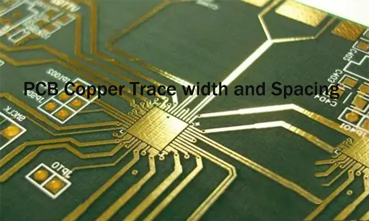
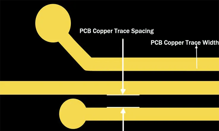
Within the discipline of printed circuit board (PCB) design, engineers often engage in the practice of making informed estimations concerning numerous facets of their design schematics. Among these critical design considerations is a parameter commonly identified as “Trace and Space.” The “Trace” component refers to the width of a designated copper pathway, whereas “Space” delineates the width of the void separating two proximate copper features. This metric is pivotal in ensuring the integrity and functionality of the PCB layout.
The determination of suitable PCB copper trace and space values takes into account multiple factors. This article presents fundamental guidelines for establishing appropriate trace and space guidelines.
The Challenges Posed by Today’s PCB Routing Technologies
Historically, the routing of traces on printed circuit boards (PCBs) was a relatively uncomplicated task, with traces being allocated standard widths and spacings, except for broader connections like power and ground vias, which were the primary exceptions. Adjustments to other trace width requirements were minimal and typically executed manually during the routing process. However, with the evolution of circuit board technology, the specifications for trace width and spacing have become significantly more nuanced and complex.
In modern PCB design practices, engineers must consider a variety of trace width and spacing requirements, such as:
●Controlled impedance routing, which demands precise widths and spacing to ensure desired signal integrity.
●High-speed traces, requiring increased spacing to mitigate interference with adjacent routing.
●Analog routing, which may have specific default width and spacing parameters.
●Power and ground connections, necessitating wider traces to support higher current loads.
●Power supplies, characterized by variable trace widths tailored to the circuit’s specific needs.
●Enhanced spacing between analog and digital routes to prevent cross-talk and maintain signal isolation.
Furthermore, the physical positioning on the circuit board influences trace width and spacing decisions, with examples including:
●Connectors, which often require finer trace widths to accommodate densely arranged pins.
●Components with fine pitch, such as quad flat packages (QFP) or small-outline packages (SOP), demanding narrower trace widths for effective escape routing.
●Ball grid arrays (BGA), where routing around pins and vias might necessitate reduced trace widths.
An essential element of PCB routing involves the strategic use of vias for layer transitions. Unlike manual layout techniques, which permitted ad-hoc adjustments, contemporary PCB design software necessitates more rigorous planning. Designers utilize a spectrum of via types and sizes depending on the routing requirements, categorized as follows:
●Thru-hole vias: These traditional vias are mechanically drilled and pass through the entire board.
●Blind and buried vias: These vias, also mechanically drilled, either partially penetrate the PCB or link internal layers, requiring advanced fabrication techniques for precise drilling and alignment.
●Microvias: Fabricated using laser technology, these vias are considerably smaller and usually connect two layers. They are particularly useful for via-in-pad applications and high-density interconnect (HDI) designs, which feature finer traces and vias.
Addressing these complexities is a fundamental challenge in the routing of sophisticated PCBs, necessitating a deep understanding of both the functional and physical constraints of circuit board design.
Copper Trace Width Determination
Determining the appropriate copper trace width in a PCB design necessitates a comprehensive evaluation of multiple factors, including current carrying capacity, temperature rise, signal integrity, and manufacturing constraints. While diverse methods and guidelines exist, here’s a foundational overview of the process:
Identify the maximum current for the trace: Begin by discerning the maximum current anticipated to flow through the trace, which may stem from specific component specifications or the overarching power distribution across the circuit.
Calculate the acceptable temperature rise: Determine the permissible temperature rise for the trace, contingent upon the operational environment and the thermal properties inherent in the PCB material. Elevated temperature rises may escalate resistance and introduce potential reliability concerns.
Utilize trace width calculators or guidelines: Leverage available online calculators or design guidelines to ascertain the appropriate trace width. These tools take into account factors such as desired current capacity, acceptable temperature rise, copper thickness, PCB material, and thermal considerations.
Consider signal integrity requirements: In designs necessitating high-speed transmission, trace width assumes significance in upholding signal integrity. The width of the trace influences its impedance, which can impact signal quality. In such instances, additional scrutiny based on the specific signal requirements becomes indispensable.
Account for manufacturing constraints: Factor in the manufacturing capabilities of the designated PCB manufacturer. Manufacturers typically delineate limitations concerning the minimum achievable trace width. It is imperative to ensure that the selected trace width aligns with manufacturing constraints to preempt any fabrication complexities.
Iterative refinement: Embrace an iterative refinement approach, wherein the determined trace width undergoes evaluation and potential adjustment based on simulation results, prototyping outcomes, or feedback from the PCB manufacturer. This iterative process facilitates the optimization of trace width in accordance with the precise design requisites and constraints.
It’s paramount to recognize that while the outlined steps offer a foundational framework, the specific determination of trace width may undergo variations contingent upon the design complexity, PCB technology utilized, and unique application requisites.
Copper Spacing Considerations
In the realm of PCB design, copper spacing considerations are crucial for maintaining signal integrity, reducing crosstalk, and adhering to manufacturing norms. Here’s an encapsulation of key aspects to consider:
Signal Integrity: The maintenance of adequate copper trace spacing has a profound effect on signal integrity, particularly in designs intended for high-speed operation. Vital considerations include:
●Crosstalk Reduction: The establishment of appropriate trace spacing aids in mitigating crosstalk, an undesirable interaction between adjacent traces. The requisite spacing fluctuates based on signal properties and the desired isolation levels to preserve signal quality and suppress noise.
●Impedance Regulation: Ensuring consistent trace spacing is integral in impedance-regulated designs to uphold the characteristic impedance of transmission routes. Uniform spacing fortifies signal integrity and constrains impedance variations.
●Differential Signals: For differential signal pairs, it’s critical to preserve consistent spacing between the positive and negative traces to maintain signal balance and minimize common-mode noise.
Production Constraints: Copper trace spacing should concur with the capabilities of the PCB fabrication process. PCB producers specify the minimal achievable trace separation due to manufacturing processes such as etching or drilling. It’s paramount to ensure that the chosen spacing falls within these restrictions to bypass fabrication complications.
Design Rules and Clearance Requirements: PCB design software provides design rule checks (DRC), permitting the specification of minimum clearance prerequisites between copper elements. Abiding by these rules ensures that the spacing between traces, pads, and other copper elements aligns with the design goals, forestalling manufacturing predicaments like short circuits or unintentional electrical links.
Environmental Factors: Environmental parameters like temperature, humidity, and electrical disruption can influence the needed copper trace spacing. Meeting specific environmental requirements or norms is vital when determining copper spacing.
High Voltage Clearances: Designs containing high-voltage circuits necessitate additional spacing to guarantee sufficient electrical insulation and prevent arcing or breakdown. Complying with safety norms and regulations is essential in such scenarios.
Component Positioning: The layout of components affects copper spacing considerations. Ample space between components is necessary to accommodate needed copper traces and uphold suitable spacing between them.
Efficiently tackling copper spacing considerations calls for thorough planning and meticulous adherence to design norms and production constraints, thereby ensuring optimal signal performance and reliability in PCB designs.
PCB Copper Trace and Space: Three Factors to Consider
In the process of designing Printed Circuit Boards (PCBs), the meticulous selection of copper trace width and spacing stands as a critical endeavor. These parameters serve as fundamental pillars shaping not only the performance but also the durability and reliability of the circuit board. Here, we outline three key factors necessitating meticulous consideration:
Current Carrying Capacity:
An essential consideration is the current carrying capacity, denoting the maximum current a trace can convey without surpassing a specified temperature rise. The width of a copper trace profoundly influences this capacity, with broader traces capable of accommodating higher currents. Guidance on trace width corresponding to particular current levels is outlined in the IPC-2221 standard. Overheating poses a substantial risk, potentially leading to PCB material degradation and eventual failure. Thus, it is imperative to ensure that the trace width aligns with the current demands of the circuit.
Impedance Control:
Impedance, defining the resistance a circuit offers to current flow when subjected to a voltage, assumes paramount importance, especially in high-frequency circuits. Maintaining consistent impedance levels is critical to mitigate signal reflection, which can detrimentally impact data integrity. Trace width, thickness, substrate dielectric constant, and the distance between the trace and ground plane collectively influence impedance. Designers must meticulously evaluate these factors, particularly when crafting high-speed or RF circuits.
Manufacturability and Cost:
Considerations of manufacturability and cost are equally pivotal. Smaller traces and spaces necessitate more precise manufacturing processes, potentially escalating production expenses. Moreover, diminutive traces are more susceptible to damage during manufacturing. Thus, there exists a delicate balance in selecting trace and space widths that are minimally requisite for circuit functionality, while acknowledging the heightened costs and susceptibility to damage associated with smaller dimensions.
By meticulously addressing current carrying capacity, impedance control, and manufacturability and cost, designers can ascertain the optimal copper trace and space configurations for their PCBs. These factors are inherently interconnected, with modifications in one parameter reverberating across others. Consequently, thorough planning and iterative design refinement are often indispensable to achieve optimal outcomes.
Design Rules and Constraints
In the present-day layout of printed circuit boards, the management of various trace widths and spacings has become a critical task. These assignments encompass individual nets, groups of nets (buses), as well as power and ground nets. Moreover, it is essential to select the appropriate vias for each assignment, and in some cases, multiple sets of values must be assigned to a single net or group. To handle this complexity, PCB design tools employ design rules and constraint management systems.
Over time, design rules and constraints have significantly evolved from the early stages of PCB design CAD tools, where control options were limited. Modern constraint management systems, such as the one depicted above, provide a spreadsheet-style interface that enables designers to establish diverse rules and constraints. The interface allows assigning different trace widths to specific nets, and by scrolling further, one can access settings for trace spacing, via assignments, and more.
These constraint management systems empower designers with comprehensive control over trace routing rules in their designs. Furthermore, these systems also govern other design aspects, including signal timing, component spacing, and manufacturability settings for solder paste and silkscreens.
In addition to rules and constraint management, contemporary CAD tools offer a broad range of routing tools that enhance a designer’s efficiency and productivity.
Conclusion
PCB copper trace and space guidelines serve as important considerations in PCB design. However, engineers must exercise their professional judgment to ensure the designs they create meet the required standards. Adequate time should be allocated for thorough field testing, and in situations where this isn’t possible, rigorous design methodologies should be employed to address potential risks. By doing so, engineers can confidently deliver high-quality designs that align with the demands of their applications.
Related Posts:
1. Selecting PCB Laminate Materials: A Comprehensive Overview
3. Which Types are Most Commonly Used in PCB Substrates?
4. What Is Fiberglass PCB and Why Fiberglass Used in PCB Manufacturing?
5. Standard PCB Thickness-Choosing the Correct Thickness for PCB