
In today’s competitive electronics industry, manufacturers and engineers are constantly searching for ways to enhance the performance, reliability, and cost-efficiency of their products. As technologies advance, more sophisticated materials are needed to meet the increasing demands of high-speed, high-frequency, and high-density applications. BT PCBs, crafted from BT epoxy resin, have emerged as an excellent solution for these challenges. These printed circuit boards (PCBs) offer substantial improvements over traditional materials, especially in environments where performance and reliability are non-negotiable.
In this article, we will dive deep into the design, manufacturing, quality, cost and assembly of BT PCBs. We’ll discuss how to optimize their use in high-frequency applications, review the best practices for their assembly, and explore pricing considerations—all while making sure you understand the unique benefits and challenges of using BT PCB material.
Introduction:
Understanding BT PCB and Their Importance in Modern Electronics
BT PCBs are built using BT epoxy resin, which offers superior thermal performance, low dielectric loss, and high dimensional stability. These qualities make BT PCBs a top choice for applications requiring high-frequency signal integrity and heat dissipation. Whether for 5G, automotive, aerospace, or medical device applications, BT PCB materials have become integral in achieving robust, long-lasting, and efficient electronic devices.
BT PCBs stand out because of their low dielectric constant and high thermal conductivity, which make them suitable for applications that require high-speed data transmission, low signal loss, and reliable thermal management. As the world continues to push toward faster communications and smaller, more compact designs, BT PCBs are ready to meet these demands with exceptional performance.
Advanced Design Principles for BT PCB
Designing BT PCBs requires a deep understanding of both the material properties and the design challenges that engineers face when creating high-performance electronic systems. These circuit boards are often chosen for high-frequency applications, where signal integrity, thermal management, and dimensional stability are non-negotiable. The unique material properties of BT epoxy resin offer significant advantages, but designing these PCBs to meet specific requirements involves careful planning and execution. Below are some of the key considerations and design principles that come into play when developing BT PCBs for cutting-edge applications.
Optimizing BT PCB for High-Frequency Applications
When you’re designing BT PCBs for high-frequency applications like 5G networks or RF circuits, you need to keep an eye on key metrics that could impact the signal integrity. The dielectric constant (Dk) is the star player here—too high, and you’ll get signal degradation. But with BT epoxy resin, you’re in luck—it offers a low Dk, keeping your high-speed signals crisp, clear, and interference-free. BT PCBs are perfect for this because of their low dielectric constant and excellent signal integrity. These properties minimize the degradation of the signal over long distances or high frequencies, allowing data transmission to remain accurate and reliable.
Signal loss is a major concern in high-frequency designs, where even small variations in impedance can lead to errors in data transmission. Engineers can control this by paying close attention to factors like trace width, spacing, and material properties. The low dielectric loss tangent of BT epoxy resin makes it a strong contender in reducing signal attenuation.
Performance Comparison of Dielectric Constants (Dk) for Common PCB Materials:
| Material | Dielectric Constant (Dk) | Signal Loss at High Frequencies | Use Case |
| BT Epoxy Resin | 3.2 – 3.4 | Low | 5G Applications, RF Circuits |
| FR4 (Standard PCB) | 4.5 – 5.0 | High | General Electronics, Consumer Products |
| PTFE (Teflon) | 2.0 – 2.3 | Very Low | High-Frequency Communications |
Here’s the lowdown: the lower the dielectric constant, the better it is at handling high-frequency signals without losing that precious data. So if you’re cranking out designs for 5G or RF communication, BT PCBs are your go-to material. FR4 and PTFE just don’t match up when you’re in the fast lane of high-speed electronics.
In 5G networks, for example, you’ll often see BT PCBs being used because they preserve signal clarity even at high frequencies. It’s like cruising on the highway at top speed with a steady hand on the wheel—no bumps or breakdowns.
Thermal Management in High-Density Circuits
As electronic devices become more compact and high-density circuits become the norm, heat management becomes a critical concern. The BT epoxy resin used in BT PCBs excels in thermal conductivity, which is necessary to keep temperatures under control in high-performance environments. High-frequency signals, combined with dense packing of components, lead to significant heat generation, which can result in thermal stress, warping, and ultimately, failure of the PCB.
For instance, in automotive electronics or aerospace systems, circuit boards often encounter extreme temperature variations. In these cases, BT PCBs provide thermal stability and reliability, ensuring that components stay within operating temperature ranges, even in harsh conditions. The low CTE (Coefficient of Thermal Expansion) of BT PCBs further ensures that the material doesn’t expand or contract significantly, reducing the likelihood of mechanical failures.
Thermal Conductivity Comparison for Different PCB Materials-
| Material | Thermal Conductivity (W/m·K) | Max Operating Temperature | Thermal Stability |
| BT Epoxy Resin | 0.3 – 0.4 | 150°C – 180°C | High |
| FR4 (Standard PCB) | 0.25 – 0.3 | 120°C – 130°C | Medium |
| Aluminum PCB | 1.0 – 2.0 | 120°C – 180°C | Very High |
For automotive and aerospace designs, where temperatures fluctuate dramatically, BT PCBs excel at managing heat with precision. Their high thermal conductivity acts like a reliable cooling system in a high-performance engine, ensuring stability even when conditions get intense. This dependable heat management makes them an excellent choice for environments that demand durability and consistent performance under thermal stress. With BT PCBs, it’s like having a steady hand on the wheel in ever-changing conditions.
In electric vehicles, for instance, BT PCBs are used in battery management systems to prevent overheating in the heart of the system—so no more worries about your EV battery catching a fever. It’s as smooth as cruising down the highway with the A/C on full blast.
Material Selection for Complex Designs
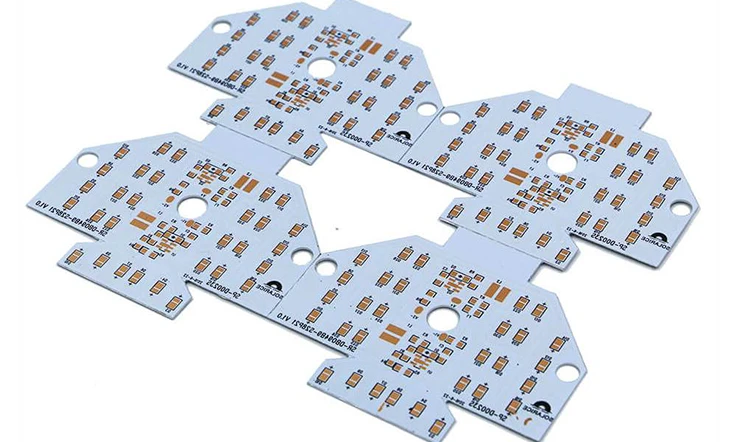
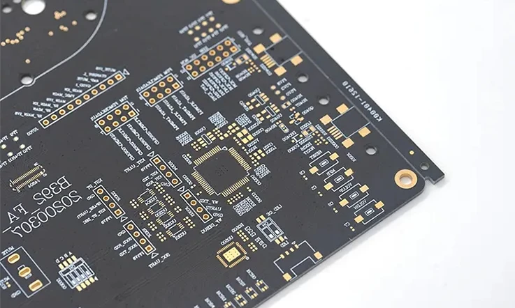
When working with multilayer BT PCBs, engineers can incorporate a range of advanced features, such as buried vias, blind vias, and controlled impedance traces, without compromising the performance of the board. BT PCBs maintain their integrity across multiple layers, ensuring the performance reliability of complex circuits.
As designs become more complex, the need for reliable multilayer PCBs increases. BT epoxy resin provides the dimensional stability required for these complex applications, offering a consistent level of moisture resistance, thermal resistance, and dielectric stability. Therefore, complex designs are like a jigsaw puzzle: every piece has to fit perfectly. And for multilayer or high-performance designs, BT PCBs have the staying power to handle it all.
Dimensional Stability & Moisture Resistance Comparison for Complex Designs-
| Material | Dimensional Stability | Moisture Absorption | Flexibility for Complex Layouts |
| BT Epoxy Resin | High | Low | Excellent |
| FR4 (Standard PCB) | Medium | Medium | Good |
| Polyimide | High | Very Low | Very Good |
If you’re diving into military or medical device applications, BT PCBs are built to last. Whether you’re making a multilayer PCB for a drone or a medical implant, BT epoxy resin can take the heat and still stand strong against moisture and environmental stress.
For medical devices, precision and durability are non-negotiable. BT PCBs shine in this field by keeping their structure rock-solid, even when temperatures or humidity levels take a wild turn. Think of it like a marathon runner who doesn’t flinch at changing weather—these boards are built to endure the long haul and handle occasional challenges without skipping a beat.
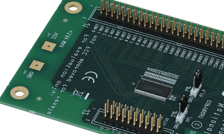
The BT PCB Manufacturing Process: Step-by-Step Guide
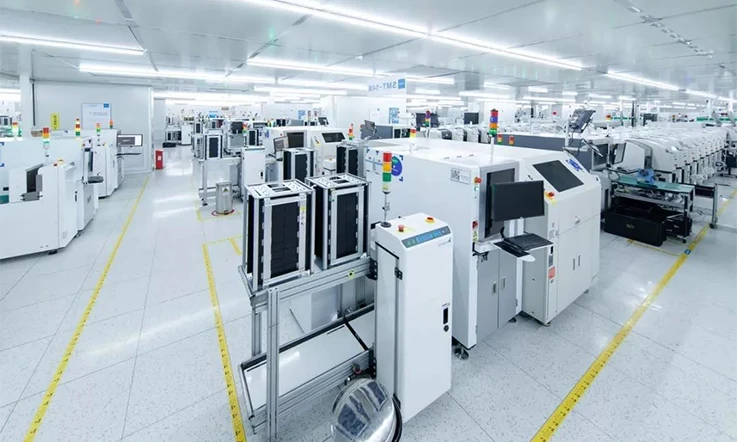
Producing BT PCBs is a meticulous process that demands precision at every stage, from selecting premium materials to conducting rigorous testing on the final product. This isn’t just about crafting a circuit board; it’s about engineering a reliable foundation for high-speed and high-frequency technologies. Applications like 5G systems, aerospace modules, and automotive electronics count on these boards to deliver peak performance under demanding conditions. Let’s dive into the nuts and bolts of the manufacturing journey and explore what sets BT PCB production apart from the rest.
Material Selection and BT Epoxy Resin Properties
The journey begins with material selection. At this stage, the choice of BT epoxy resin is key. Unlike traditional materials such as FR4, BT resin is preferred in high-frequency applications because of its low dielectric loss and strong thermal stability.
For high-speed circuits, material properties like signal integrity, moisture resistance, and thermal conductivity must be prioritized. The unique composition of BT epoxy resin makes it a perfect choice for demanding environments where signal transmission and temperature control are non-negotiable.
Comparison of BT Epoxy Resin and Other PCB Materials-
| Material | Dielectric Loss (Tan δ) | Thermal Conductivity | Moisture Absorption |
| BT Epoxy Resin | 0.003 – 0.004 | 0.3 – 0.4 W/m·K | Low |
| FR4 | 0.02 – 0.03 | 0.25 W/m·K | Medium |
| Polyimide | 0.004 – 0.01 | 0.3 – 0.4 W/m·K | Very Low |
BT epoxy resin stands out with its low dielectric loss, meaning less signal degradation during high-frequency operations. It’s like picking the best tires for your car—choose wisely, and you’ll keep everything running smoother and faster.
In high-speed PCB designs, such as those for 5G and RF circuits, BT PCBs stand out for their ability to preserve signal clarity even at higher frequencies. The low dielectric loss of the material minimizes energy dissipation, allowing for faster data transmission without compromising signal stability. Think of it as giving your signal a clear, open highway with no speed traps—effortless flow and reduced interference. This property ensures your design can tackle the demands of modern communications with efficiency and precision.
Fabrication Steps: From Design to Final Product
The process begins with laminating the layers of BT epoxy resin onto the substrate. From there, laser drilling is used to create precise holes for vias and other interconnections. The key to successful BT PCB fabrication lies in maintaining precise registration between the layers during the lamination process. This ensures that the PCB will maintain its integrity under stress and high-frequency conditions.
After the layers are stacked and bonded together, the next step is etching. This is where the actual circuit patterns are created, followed by plating and solder masking. Once the final etching is complete, quality testing begins, ensuring that the BT PCB meets all specifications for electrical conductivity and thermal performance.
Step-by-Step Process in BT PCB Fabrication-
1.Lamination: Layers of BT epoxy resin are bonded onto a base material, forming the foundation of the PCB.
2.Drilling: Laser drilling is used to create precise via holes for interlayer connections.
3.Etching: The circuit pattern is etched onto the layers, defining the paths for electrical current.
4.Plating and Solder Masking: Plating is applied to the etched circuit to ensure conductivity, and a
5.solder mask is added to protect the traces during assembly.
6.Inspection and Testing: After the PCB is fully fabricated, it undergoes rigorous testing to ensure it meets electrical performance and thermal management standards.
The challenge in this process is maintaining precise registration of each layer during lamination. Any misalignment can lead to malfunctioning circuits. Think of it as stacking a deck of cards—if you don’t line them up properly, the whole structure could collapse.
Overview of the Etching Process-
| Step | Purpose | Key Considerations |
| Lamination | Bond BT epoxy resin layers | Thickness, uniformity |
| Laser Drilling | Create vias and interconnections | Precision, drill diameter |
| Etching | Define circuit paths | Chemical bath, time, temperature |
| Plating & Masking | Apply metal plating, solder mask | Consistency, protection |
Quality Control and Reliability Testing
Once fabrication is complete, it’s time for quality control. Every BT PCB goes through a battery of tests to ensure it meets the required standards. These tests simulate real-world conditions, ensuring that the PCB can handle the stresses of both temperature fluctuations and high-speed operation.
A major part of the testing is thermal cycling, which exposes the PCB to extreme heat and cold to see how well it handles thermal expansion and contraction. This ensures that the PCB will maintain its structural integrity over time, even in harsh environments such as automotive or aerospace applications.
Comparison of Reliability Testing for Different PCB Materials-
| Test | BT Epoxy Resin | FR4 | Polyimide |
| Thermal Cycling | Passed 1000+ cycles | Passed 500-1000 cycles | Passed 1500+ cycles |
| Moisture Resistance | Low Absorption | Medium Absorption | Very Low Absorption |
| Signal Integrity | Excellent, low loss | Moderate, some loss | Excellent, low loss |
BT PCBs are engineered to perform under extreme conditions, and their reliability is confirmed through rigorous thermal cycling tests. These evaluations demonstrate how well the boards endure repeated exposure to fluctuating high temperatures, ensuring their performance remains consistent. For instance, the BT epoxy resin’s exceptional thermal stability keeps the board structurally sound and maintains signal clarity, even in demanding applications like aerospace and automotive systems. It’s like putting a car through a grueling endurance test to guarantee it can handle every twist and turn without a hiccup.
BT PCBs aren’t just reserved for cutting-edge technologies—they’ve proven their mettle in consumer electronics too. Whether it’s a smartphone enduring hot summers and damp environments or a home device stationed in less-than-ideal conditions, these boards hold their ground. The BT epoxy resin used in their construction offers exceptional durability, shrugging off temperature swings and moisture exposure like it’s no big deal. Designing with this material is like gearing up for an adventure—you know your equipment can handle the bumps and unexpected weather along the way.
Assembly Considerations for BT PCB
Once your BT PCB is manufactured, the next step is assembly, which is where things start to come together. But, assembling BT PCBs isn’t the same as assembling your standard FR4 boards. BT PCBs come with their own unique set of challenges and advantages—especially when it comes to high-speed applications, thermal management, and high-frequency designs.
Because BT epoxy resin has superior thermal conductivity and a higher Tg (glass transition temperature), the assembly process must be carefully considered to ensure the finished product holds up to demanding environments. Let’s dive into some key assembly considerations to keep in mind when handling BT PCBs.
Handling High-Temperature Soldering
Soldering a BT PCB requires precision, especially during high-temperature processes. Thanks to the high Tg (glass transition temperature) of BT epoxy resin, these boards can withstand elevated soldering temperatures without compromising their structural integrity. This characteristic is particularly beneficial in industries like automotive and military, where lead-free soldering is a standard practice, and components need to endure extreme heat. Essentially, BT PCBs can hold their own even in the hottest conditions, ensuring reliable performance without warping or degradation. Whether you’re assembling complex automotive electronics or military-grade devices, these boards are designed to perform under pressure.
Unlike traditional FR4 boards, BT PCBs maintain their strength and resist warping even after being exposed to high soldering temperatures. This ability to handle heat makes them well-suited for more demanding applications, ensuring long-term reliability and performance, even under extreme conditions.
Example: Soldering Process for BT Epoxy Resin Boards-
| Material | Tg (Glass Transition Temperature) | Maximum Soldering Temperature | Lead-Free Solder Compatibility |
| BT Epoxy Resin | 180°C – 250°C | 260°C | Yes |
| FR4 | 130°C – 150°C | 250°C | Yes |
| Polyimide | 250°C – 300°C | 300°C | Yes |
BT PCBs can withstand soldering temperatures up to 260°C, making them the go-to material when working with high-performance applications that demand heat resilience. So, whether you’re working on automotive electronics or aerospace, BT PCBs are built to handle the heat.
The key here is ensuring that soldering temperatures are optimized to avoid damaging the PCB or compromising its thermal stability. With BT PCBs, you’ve got a board that’s tough and ready for whatever the assembly line throws at it.
Maintaining High-Speed Performance During Assembly
When it comes to high-speed performance, maintaining clear signal paths is key. During Surface Mount Technology (SMT) assembly, it’s all about ensuring each component and connection is aligned perfectly. We must pay attention to detail to avoid any misalignments that could interfere with the flow of signals. Even small discrepancies can cause issues with signal integrity, resulting in slower speeds or data loss. The precision required in this process means that every step—whether it’s placing components or soldering—is done with care to ensure that signals stay clean and uninterrupted. Think of it like tuning a high-performance engine—everything needs to be just right to keep things running at top speed.
In high-frequency applications like 5G and RF circuits, the game is all about managing impedance and minimizing signal loss. This is where BT PCBs really stand out. With the low dielectric loss of BT epoxy resin, they keep the signal clear and uninterrupted even as high-speed signals rush across the board.
For example, in 5G applications, where signals are pushed to their limits, BT PCBs excel in keeping the transmission clean and fast. So, if you’re working on cutting-edge communications technology, BT PCBs will keep your signals in tip-top shape, avoiding signal degradation.
Example: Impedance Control in High-Speed Applications-
| Material | Dielectric Constant (Er) | Dielectric Loss (Tan δ) | Signal Integrity |
| BT Epoxy Resin | 3.0 – 3.2 | 0.003 – 0.004 | Excellent (Low Loss) |
| FR4 | 4.0 – 4.5 | 0.02 – 0.03 | Moderate (Some Loss) |
| Polyimide | 3.0 – 3.3 | 0.01 – 0.02 | Good (Moderate Loss) |
With a low dielectric loss, BT PCBs ensure that even high-frequency signals stay strong and intact. This makes them ideal for industries that require ultra-fast data transmission, like telecommunications and aerospace. So when you’re designing circuits for applications that rely on speed and signal integrity, BT PCBs provide the reliability you need.
Managing Common Assembly Issues
When assembling BT PCBs, we need to stay on their toes. Common assembly issues, like warpage or via misalignment, can occur, especially when working with high-performance boards. But don’t worry, there are ways to manage and avoid these issues.
For instance, because BT epoxy resin has high thermal stability, it reduces the risk of warping or deformation during the assembly process. However, the handling of BT PCBs should be done with care to avoid any unnecessary stress that could cause distortion. Additionally, precision is key during the drilling process, as any misalignment of vias can lead to faulty connections. Ensuring that the layers align perfectly will keep everything running like clockwork.
To catch any potential problems early, Automated Optical Inspection (AOI) systems can be employed to detect misalignments, soldering defects, or even signal trace issues that could compromise the board’s functionality. Early detection helps ensure that only the highest-quality BT PCBs make it to the final product.
Example: Handling Warpage and Misalignment-
| Assembly Issue | Cause | Solution |
| Warpage | Thermal expansion mismatch | Use high-Tg materials like BT epoxy resin |
| Via Misalignment | Poor drilling precision | Employ laser drilling for precise via holes |
| Soldering Defects | Improper soldering temperature | Optimize soldering temperature and use lead-free solder |
By properly managing these challenges, we can prevent potential failures and ensure the reliability of the assembled BT PCBs. When it comes to high-performance applications, precision is everything, and even the smallest misstep can lead to failure.
Pricing Strategies and Cost Factors in BT PCB Projects
When you’re diving into BT PCB pricing, it’s not all about the bottom line. Of course, cost is top of mind for most projects, but finding the sweet spot between cost and performance can make or break the final product. Understanding the factors that influence BT PCB pricing helps ensure that you’re not only sticking to your budget but also getting the quality and reliability your project needs. Whether it’s material quality, layer count, or specific design requirements, each element contributes to the final price tag. In this section, we’ll break down what drives the costs of BT PCBs and offer some tips on how to make smart pricing decisions that won’t stretch your wallet.
Breakdown of Cost Factors in BT PCB Fabrication
The price tag for BT PCBs isn’t just pulled out of thin air. Several factors contribute to the overall cost, and as you might expect, materials lead the charge.
1.Material Costs-
BT resin is more expensive than the standard FR-4 material, but that’s because it delivers superior performance. The resin’s high glass transition temperature (Tg), low dielectric loss, and thermal stability make it ideal for high-frequency, high-speed applications like 5G networks and automotive electronics. This added performance comes with a higher upfront price, but when you consider the long-term benefits, the investment is worth every penny.
2.Complexity of Design-
The number of layers in your PCB design directly affects the cost. More layers mean more lamination, drilling, and etching steps, all of which increase the time and labor involved in the process. Additionally, special via types (like blind vias or buried vias) and surface finishes such as gold plating can raise prices. The more complex your design, the more costly the manufacturing process will be.
3.Customization-
Custom features, like special flexibility or high-density interconnects (HDI), come at a premium. Customizing your BT PCB to fit unique dimensions, shapes, or performance specifications also adds to the cost.
Example: Cost Comparison of Material Types
| Material Type | Cost per Square Inch | Thermal Stability | Application Suitability |
| BT Epoxy Resin | Higher | Excellent (Up to 250°C) | High-speed, high-frequency |
| FR-4 | Lower | Moderate (Up to 130°C) | General-purpose electronics |
| Polyimide | Higher | Excellent (Up to 300°C) | Aerospace, military |
As shown, BT resin costs more than FR-4, but for those high-performance applications, the benefits are clear. Investing in BT PCBs now can save you from costly failures down the road.
Cost Optimization Through Volume Manufacturing
Planning a big project? If mass production is in your future, buying in bulk can save you some serious cash. The key to cutting down costs per unit is ramping up production volume. Here’s the deal: when you buy in large quantities, you’re spreading out the setup costs over more units, which drops the cost per piece. It’s like buying in bulk at a warehouse store—you’re paying less per item because you’re buying more. For BT PCBs, this means less overhead and a more affordable per-unit price as you ramp up your production. Plus, working with a PCB manufacturer – JarnisTech that offers volume discounts can really help keep your budget in check.
1.Economies of Scale-
When you place large orders, we can spread their fixed costs (such as setup, tooling, and process development) over many units, significantly lowering the per-unit cost. If you’re ramping up for a large-scale project, whether it’s a series of consumer electronics or industrial equipment, negotiating high-volume pricing with us can help drive down overall expenses.
2.Streamlined Production-
Once the production process is dialed in for a large batch, the time and labor required for subsequent units decreases. The more efficient the production process, the lower the labor cost per unit. This efficiency translates into better cost optimization, making BT PCBs more affordable on a per-unit basis as production increases.
Example: Volume Manufacturing vs. Small Batch
| Order Size | Cost per PCB (USD) | Lead Time | Production Complexity |
| Small Batch | High (Higher setup cost) | Longer | Custom designs |
| Volume Orders | Low (Economy of scale) | Shorter (Optimized) | Streamlined |
As you can see, volume manufacturing can dramatically lower the price per unit. So if you’ve got a larger order on the horizon, consider making the most of those bulk discounts.
Long-Term ROI of BT PCB in Specialized Applications
It might be tempting to focus solely on initial costs, but when it comes to BT PCBs, long-term ROI is where the real story lies. While BT PCBs may have a higher upfront cost, their reliability and thermal stability make them an excellent investment for specialized applications, leading to savings down the line.
1.Reduced Downtime and Failures-
The high thermal conductivity and low dielectric loss of BT PCBs help ensure fewer failures during use, which means less downtime for the devices in which they’re used. This is a huge benefit in mission-critical applications such as military electronics, medical devices, and automotive systems, where failure rates need to be kept to an absolute minimum.
2.Lower Maintenance Costs-
Since BT PCBs are built to withstand higher temperatures and more demanding environments, they require less frequent repairs or replacements. This reduces overall maintenance costs and increases the lifespan of the final product, which adds to the long-term cost savings.
Example: ROI Calculation in High-Performance Applications
| Material | Upfront Cost | Expected Lifespan | Maintenance Cost (Annually) | Total Lifetime Cost |
| BT Epoxy Resin | High | 10+ years | Low | Low |
| FR-4 | Low | 5-7 years | High | High |
In the long run, BT PCBs offer more value, despite the higher upfront cost. When you factor in maintenance costs, failures, and product lifespan, the return on investment for BT PCBs becomes clear. Investing in BT PCBs now can save you from future expenses and increase the product’s overall value.
How Ensuring Quality and Reliability in BT PCB Production?
When working with BT PCBs, ensuring top-notch quality and reliability is non-negotiable—especially for engineers and project managers overseeing complex and high-performance applications. From aerospace components to 5G communication modules, quality assurance in BT PCB production ensures that your product not only meets expectations but surpasses them. Let’s dive into the key aspects of ensuring quality and reliability at every step of the BT PCB production process.
Certifications and Industry Standards for Quality Assurance
Quality certification is more than just a nice-to-have; it’s a must-have when choosing a BT PCB supplier. Certifications like ISO 9001, UL, and RoHS compliance are the baseline for ensuring your boards meet stringent industry standards.
1.ISO 9001 Certification-
ISO 9001 guarantees that the PCB manufacturer has a consistent, reliable, and traceable quality management system in place. This certification covers everything from initial design to the final inspection, ensuring that the BT PCBs are produced with precision and adhere to international standards.
2.UL Certification-
UL (Underwriters Laboratories) certification ensures that the BT PCBs meet fire safety standards, critical for industries like automotive and medical devices, where safety cannot be compromised. UL-listed BT PCBs undergo rigorous testing for flammability, ensuring they can handle extreme temperatures without posing a risk.
3.RoHS Compliance-
RoHS compliance ensures that your PCBs are free from hazardous materials such as lead, mercury, and cadmium, which can have harmful effects on both human health and the environment. By choosing a PCB manufacturer- JarnisTech with RoHS certification, your BT PCB circuit boards will meet strict environmental and safety standards. This is especially critical if you’re targeting markets like Europe, where strict regulations enforce the use of eco-friendly materials. It’s a smart move for both compliance and sustainability, showing that your products are designed with care for both the planet and your customers’ well-being.
4.IPC-6012 Standards-
The IPC-6012 standard specifies the requirements for printed circuit boards used in electronics. It’s especially valuable for BT PCBs, where the manufacturing process requires precise layering and reliable electrical connectivity. By following this standard, we ensure BT PCBs meet performance and durability requirements in demanding applications.
Example: Certifications Table
| Certification | What It Covers | Why It Matters |
| ISO 9001 | Quality management system | Ensures consistency and high production standards |
| UL Certification | Fire safety and electrical standards | Critical for automotive and medical safety standards |
| RoHS Compliance | Restriction of harmful substances | Ensures eco-friendliness and meets global regulations |
| IPC-6012 | PCB manufacturing and acceptability | Ensures durability and performance for advanced electronics |
As you can see, these certifications aren’t just fancy labels—they’re the foundation for ensuring BT PCB quality and reliability in real-world applications.
Testing and Validation for Extreme Environments
Testing is a vital step in ensuring that BT PCBs can withstand extreme environments. Whether it’s a military-grade application that needs to endure extreme temperatures or a high-speed 5G module that requires rock-solid electrical performance, the right tests must be conducted to guarantee product integrity.
1.Thermal Cycling-
For applications in aerospace or military electronics, thermal cycling testing is a must. This process subjects the BT PCB to rapid temperature fluctuations, simulating real-world thermal expansion and contraction. This helps ensure that the PCB can perform without failure in extreme temperature environments, from freezing cold to scorching heat.
2.Vibration Testing-
Vibration testing is essential for products used in vehicles, satellites, or other moving machinery. By simulating the shock and vibration a PCB will face in real-world conditions, we can identify weak spots in the board’s design that might lead to failure.
3.Moisture Resistance-
Moisture is a silent troublemaker when it comes to electronics, especially for demanding fields like aerospace and military. For aerospace and military applications, moisture resistance testing ensures that BT PCBs can withstand high-humidity environments without compromising performance. This is done through methods such as humidity chamber testing or moisture absorption testing to simulate exposure to water and ensure that the boards stay dry and functional under extreme conditions.
4.Electrical Testing for High-Frequency Stability-
Electrical testing in 5G modules ensures that signal integrity is maintained across the board. With high-frequency applications, even a slight variation in impedance can lead to signal degradation. Tests like time-domain reflectometry (TDR) and scattering parameters (S-parameters) measure signal loss and impedance mismatch, ensuring the board performs optimally.
Example: Testing Table
| Test Type | Purpose | Applications |
| Thermal Cycling | Simulates temperature extremes | Aerospace, automotive, military |
| Vibration Testing | Tests mechanical integrity under movement | Satellites, vehicles, machinery |
| Moisture Resistance | Assesses durability in high-humidity conditions | Outdoor electronics, military, aerospace |
| Electrical Testing | Ensures signal stability and impedance accuracy | 5G modules, high-speed circuits, communication systems |
Through rigorous testing, you can rest easy knowing that your BT PCBs are prepared to meet the demands of any high-performance application.
Monitoring Signal Integrity and Impedance Control
Signal integrity and impedance control are two of the most key factors in high-speed PCB designs. Without proper management, signal degradation can lead to data loss or system failure, especially in 5G, medical devices, and automotive electronics.With high-speed circuits, even a small impedance mismatch can throw off the entire system, leading to poor signal quality or failure to communicate properly. Proper impedance control ensures that electrical signals flow without interference, making it a game of precision where any misstep could cause a hiccup in performance. It’s all about making sure the current doesn’t get lost in translation, and everything stays on track—no static, no noise, just clean, fast signals that work when you need them to.
1.Time-Domain Reflectometry (TDR)-
TDR is a technique used to measure the impedance of the PCB and identify areas where signal loss or reflection could occur. By sending a pulse down the transmission line and observing the return signal, engineers can pinpoint imperfections in the design that may cause issues in high-speed communication.
2.Scattering Parameters (S-parameters)-
S-parameters provide another method for analyzing how signals propagate through the PCB. These parameters help determine the transmission line characteristics and how much signal is lost, providing invaluable data for improving design quality, especially in high-frequency applications like 5G.
3.Automated Optical Inspection (AOI)-
AOI is an automated process that uses optical systems to inspect the BT PCB for visible defects. These can include misalignments or soldering issues, which could negatively impact performance. By using AOI early in the production process, we can detect and correct issues before they affect the final product.
Example: Signal Testing Comparison
| Testing Method | What It Measures | Why It’s Used |
| TDR | Impedance mismatch, signal reflections | Ensures signal integrity in high-speed circuits |
| S-parameters | Transmission line characteristics, signal loss | Helps optimize high-frequency performance |
| AOI | Visual inspection for defects, misalignments | Prevents defects from making it to the final product |
These testing techniques are your secret weapons to ensuring that the BT PCB performs flawlessly, even under the most demanding conditions.
Lead Times and Delivery Optimization for BT PCB Production
When you’re dealing with BT PCB production, timing is everything. Whether you’re working on a high-speed consumer electronic device or a military-grade project, delivery speed can make or break a project. Navigating the complexities of lead times and ensuring timely delivery demands a strategic approach, as every hour counts in high-demand industries. Let’s break down the factors that affect BT PCB production lead times and explore ways to optimize delivery for your project.
Impact of Design Complexity on Lead Times
When you’re dealing with BT PCBs, design complexity is the first thing that can slow down the clock. Multilayer stack-ups, complex vias, and specialized materials all contribute to longer production timelines. Let’s dig deeper into these elements:
1.Multilayer Stack-ups-
A multilayer PCB involves multiple layers of conductive material and insulation, stacked together. The more layers your design has, the longer it takes to laminate and etch each one with precision. Depending on the number of layers and their interconnects, lead times can vary significantly. For example, a 4-layer PCB might take just a few days, but a 12-layer PCB can stretch production time by weeks.
2.Complex Vias and Drilling-
Vias—small holes in the PCB that allow electrical connections between layers—can also slow things down, especially when you’re dealing with blind or buried vias. These types of vias require more precision and often involve advanced laser drilling techniques, which can add days to the production process.
3.Specialized Materials-
BT epoxy resin is a great material for high-performance applications, but sourcing these specialized materials can take time. we must ensure they have the right stock or source it from specialty suppliers, which might introduce delays. To speed things up, PCB manufacturers may need to keep these materials in inventory or establish faster supply chains.
Example: Design Complexity vs. Lead Times
| Design Factor | Impact on Lead Time | Example Application |
| Multilayer Stack-ups | Each additional layer increases production time by days. | High-frequency or multi-functional devices |
| Complex Vias | Advanced drilling techniques can add a few extra days. | Aerospace or military-grade PCBs |
| Specialized Materials | Material sourcing can introduce delays if inventory is low. | 5G modules or medical devices |
To streamline production, it’s a good idea to minimize complexity where possible, but if your project demands a complex design, ensure you’re partnering with a manufacturer that has the capabilities to handle these challenges quickly.
Optimizing Delivery Times Through Strategic Partnerships
One of the best ways to reduce lead times is through strategic partnerships with manufacturers -JarnisTech that offer services like rapid prototyping and custom BT PCB solutions. By working closely with us that understand your timeline, you can improve delivery times without sacrificing quality. Let’s break down how these partnerships work:
1.Rapid Prototyping-
Rapid prototyping allows for quick turnaround on initial designs, enabling faster iterations. In fast-paced industries like automotive and consumer electronics, where product timelines are tight, rapid prototyping can help our clients identify and fix issues before they go into full-scale production, saving valuable time. Working with a PCB manufacturer (JarnisTech) that offers this service can speed up the overall process.
2.Custom BT PCB Solutions-
Every project is different. Some applications require specialized materials or design considerations,we offer custom solutions services to meet your specific needs. Whether it’s ensuring your BT PCBs perform well at high frequencies or optimizing for specific thermal environments, having a Jarnistech means faster development cycles.
3.Long-term Collaborative Relationships-
When you have a long-standing relationship with a trusted manufacturer (JarnisTech), we can become an extension of your team. This means that we already understands your expectations, preferences, and production processes, so there’s less back-and-forth during the ordering process. As a result, we can prioritize your projects and ensure on-time delivery, even for complex or large-volume orders.
Example: Strategic Partnerships Benefits
| Partnership Type | Benefit to Lead Time | Example Outcome |
| Rapid Prototyping | Quick iterations, faster problem-solving. | Shortened design-to-production cycle |
| Custom Solutions | Tailored materials/designs speed up production. | Better product fit, fewer delays |
| Long-term Collaboration | Manufacturer familiarity reduces lead time and increases reliability. | More efficient production, priority status |
Establishing a strong partnership with the right manufacturer can make all the difference when you’re looking to accelerate your project timelines. Reach out to trusted supplier (JarnisTech), we offer rapid prototyping and custom solutions to ensure faster deliveries.
Managing Delivery for Time-Sensitive Applications
For time-sensitive applications like those in automotive, medical devices, and consumer electronics, missed deadlines aren’t an option. Here’s how you can optimize delivery for these high-demand industries:
1.Expedited Shipping-
Once your BT PCB is ready, expedited shipping can ensure it gets to you in record time. we offer express delivery services that shorten shipping times, which is perfect for projects with tight deadlines.
2.Buffer Stock and Pre-production Planning-
When you know a project’s launch is coming up, it’s wise to establish buffer stock with your manufacturer -JarnisTech. This is especially helpful for high-volume projects. Pre-ordering certain materials or parts can reduce delays, as we will already have everything in place to ramp up production when needed.
3.Prioritizing Production for Urgent Orders-
PCB Manufacturer(JarnisTech) can offer a priority production option for time-sensitive applications. By paying a premium or negotiating a rush order, you can have your BT PCBs put at the front of the line, ensuring faster manufacturing and assembly.
Example: Delivery Time Optimization
| Delivery Strategy | Impact on Delivery Times | Industry Application |
| Expedited Shipping | Shortens the time from production to delivery. | Medical devices, consumer electronics |
| Buffer Stock | Minimizes delays by preparing ahead of time. | Automotive, high-volume production |
| Priority Production | Ensures your project is prioritized in the production queue. | Aerospace, military, or time-sensitive products |
For projects that absolutely can’t wait, leverage priority production or expedited shipping to meet those tight deadlines. Be proactive and ensure you have everything ready ahead of time, and you’ll avoid those last-minute scrambles.
Why JarnisTech Should Be Your Trusted Partner for BT PCB?
Looking for a trusted partner to craft top-notch BT PCBs for your cutting-edge applications? Look no further than JarnisTech, the one-stop solution for BT circuit board manufacturing. With years of expertise, certifications that speak volumes about our commitment to quality, and access to the finest materials, JarnisTech stands ready to turn your project into a success story. Here’s why we’re the right choice for you:
1.Unmatched Expertise Spanning Over a Decade
At JarnisTech, experience isn’t just a word—it’s a foundation. With more than 10 years of hands-on involvement in BT-epoxy PCB prototyping and production, we’ve mastered the intricacies of this advanced material. Our team is well-versed in managing the precise curing processes required for BT resins, ensuring that your PCBs deliver exceptional thermal stability and performance in even the most demanding environments.
Case in Point: Precision in High-Speed Applications-
A recent project for a telecom client showcased our expertise in Fabrication high-layer-count BT PCBs for 5G base stations. Through meticulous process control, we delivered prototypes with a remarkably low dielectric loss, meeting strict signal integrity requirements and exceeding client expectations.
2.Backed by Industry-Leading Certifications
We don’t just promise quality; we prove it. JarnisTech’s manufacturing facilities adhere to globally recognized standards to ensure our BT PCBs meet the demands of specialized industries:
●UL Compliance – Rest assured, safety is embedded in every PCB we produce.
●RoHS Certification – Environmental responsibility is at the heart of our processes.
●ISO 9001 – A testament to our unwavering commitment to consistent quality.
●ISO 13485 – Designed to support the rigorous demands of medical devices.
●IATF 16949 – Meeting the precise standards of the automotive industry.
These certifications position us as a reliable partner for projects requiring strict adherence to safety, performance, and sustainability standards.
3.Strategic Partnerships with Top BT Substrate Suppliers
The backbone of any BT PCB is the substrate, and we work exclusively with renowned suppliers like Mitsubishi Gas Chemical and Isola. These collaborations ensure that every board we produce starts with the highest-grade materials.
Why It Matters: The Material Advantage-
Using premium substrates doesn’t just enhance durability; it also improves high-frequency performance, minimizes signal loss, and guarantees long-term reliability. When paired with our state-of-the-art manufacturing techniques, the result is a PCB that meets and exceeds industry benchmarks.
4.Customized Solutions Tailored to Your Needs
Every project has unique requirements, and JarnisTech is equipped to handle them all. Whether it’s a rapid prototype for a product launch or a large-scale production run for an established design, we offer:
●Flexible Layer Configurations – From simple two-layer designs to complex multi-layer stack-ups.
●Advanced Vias and Interconnects – Including blind, buried, and through-hole vias for intricate designs.
●Thermal Management Solutions – Optimized for heat dissipation in high-performance devices.
Pro Tip for Engineers: Share your design specifications early, and we’ll collaborate closely to fine-tune the production process, saving you both time and cost in the long run.
FAQs about BT PCB
What are the advantages of BT PCB over FR-4?
BT PCBs provide better thermal stability, lower dielectric loss, and enhanced performance in high-speed circuits.
In what applications are BT PCB commonly used?
They are widely used in 5G infrastructure, RF communications, automotive electronics, aerospace, and medical devices.
How does BT resin improve thermal management?
BT resin offers superior thermal conductivity, minimizing heat buildup in densely packed designs.
What challenges are associated with assembling BT PCBs?
BT PCBs require precise handling due to their thermal properties and need specialized processes for soldering and impedance control.
Can BT PCBs support multilayer designs?
Yes, BT PCBs are well-suited for multilayer configurations due to their excellent dimensional stability and resistance to warping.
What affects the cost of BT PCB?
Costs depend on material quality, layer complexity, manufacturing scale, and the use of advanced features like microvias.
What certifications should I look for in a BT PCB manufacturer?
Look for certifications like ISO 9001, RoHS compliance, UL, and industry-specific standards like ISO 13485 for medical devices or IATF 16949 for automotive.


