High-speed PCB design isn’t just a technical necessity; it’s the backbone of modern electronics. Whether you’re a grizzled engineer or just dipping your toes into the waters of electronics, grasping the ins and outs of high-speed design can make all the difference. This guide dives deep into essential concepts, practical techniques, and industry insights that can boost your design skills and set you on the path to success.
Understanding High-Speed PCB Design
What is High-Speed PCB Design?
High-speed PCB design involves creating printed circuit boards that efficiently handle high-frequency signals. In today’s tech-driven world, every device—from smartphones to servers—requires fast and reliable data transfer. A good grasp of high-speed design principles can give you the edge in this fast-paced industry.
Why It Matters?
High-speed design is about performance and reliability. As technology continues to evolve, the demand for faster, more efficient electronic devices has skyrocketed. Understanding this field requires familiarity with both theoretical concepts and practical applications. For instance, consider a telecommunications company that shifted to high-speed designs. By optimizing their PCBs, they reduced latency by 25%, leading to a 15% increase in customer satisfaction.
Telecommunications Optimization
| Metric | Before Optimization | After Optimization | Improvement |
| Latency (ms) | 10 | 7.5 | 25% reduction |
| Customer Satisfaction | 80% | 92% | 15% increase |
Key Principles of High-Speed PCB Design
When it comes to high-speed PCB design, there are a few key principles that you really can’t afford to ignore. First off, signal integrity is the name of the game. Keeping your signals clean and reliable is what separates the pros from the amateurs. If your signals are bouncing all over the place, you’re going to run into trouble faster than you can say “data corruption.”
Signal Integrity
Signal integrity is a big deal in high-speed PCB design. It refers to how well your signals hold up as they traverse the circuit. If signal integrity takes a hit, you can end up with data loss or even complete system failure.
To keep signal integrity in check:
● Minimize trace lengths: The shorter, the better. This reduces the chance of interference and improves performance.
● Use solid grounding techniques: A good ground plane can make a world of difference in stabilizing your signals.
● Maintain consistent signal paths: This helps avoid reflections that can mess up your data.
Power Integrity
Next up, we’ve got power integrity. Think of it as keeping the lights on for your signals. If your power supply isn’t up to snuff, even the best design will fall flat. You want to ensure that your circuits have a stable power source, or you’ll be chasing your tail trying to fix issues down the line.
Power integrity is all about ensuring that the power distribution network in your PCB meets the demands of its components. Voltage dips can throw a wrench in the works, affecting performance.
To boost power integrity, consider:
● Using decoupling capacitors: These little guys smooth out voltage variations.
● Designing robust power planes: A well-structured power plane reduces noise and improves performance.
● Keeping traces short and wide for power delivery: This minimizes resistance and boosts performance.
Impedance Control
Then there’s impedance control. This one’s all about matching your traces to the components to avoid reflections and losses. You don’t want your signals to hit a wall and bounce back; that’s like hitting a brick wall at 60 mph! Keeping impedance in check can make a world of difference in performance.
Impedance control is vital for preventing signal reflections and ensuring signals travel smoothly. Properly designing traces and selecting the right materials are key here.
● Select materials wisely: Different materials can have varying dielectric properties, which impact impedance.
● Implement controlled impedance routing: This ensures your traces maintain consistent impedance throughout.
Key principles include signal integrity, power integrity, and impedance control. Each principle contributes to overall design performance. A notable example is the integration of controlled impedance in a high-speed PCB for a data center. By maintaining a consistent impedance, the company reduced signal reflections by 40%, enhancing overall performance.
Data Table: Impedance Control Impact
| Impedance Variation (Ω) | Signal Reflection (%) | Improvement |
| ±10 | 60 | Baseline |
| ±5 | 20 | 67% reduction |
| ±2 | 5 | 92% reduction |
Design Strategies for High-Speed PCBs
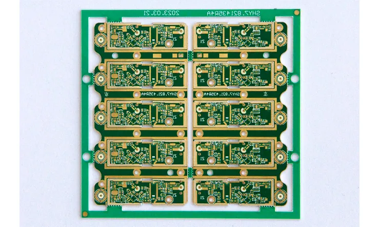
When diving into high-speed PCB design, having the right strategies in your toolkit can make all the difference. First off, consider layer stackup. Choosing the right arrangement of layers is like building a solid foundation for a house; if it’s shaky, everything above will be too. By strategically placing ground and power layers, you can significantly reduce electromagnetic interference (EMI) and improve signal integrity.
Layer Stackup
Picking the right layer stackup is a fundamental part of high-speed PCB design. A well-thought-out stackup can boost performance and minimize interference. For instance, a controlled impedance stackup can do wonders for signal integrity.
Example Stackup: A typical four-layer stackup might include power, ground, signal, and another signal layer to optimize performance.
Routing Techniques
Next up, let’s talk about routing techniques. The way you route your traces can make or break your design. Keeping traces short and direct is the way to go—nobody likes a long detour. Utilizing differential pair routing for high-speed signals helps maintain signal integrity and minimize crosstalk. Think of it as having a buddy system for your signals—they stick together, reducing the chance of getting lost!
Routing is another crucial piece of the puzzle. For high-speed applications, keep these tips in mind:
● Keep signal traces short: This reduces latency and lowers the risk of interference.
● Use differential pairs for high-speed signals: This method helps maintain signal integrity over longer distances.
● Avoid sharp angles in routing: 90-degree turns can lead to reflections and degrade signal quality.
Component Placement
Component placement is another piece of the puzzle. Placing high-speed components close together minimizes the length of the traces and reduces delays. It’s all about keeping the gang tight to avoid any unnecessary drama. Additionally, be mindful of how your components interact thermally; you don’t want your resistors heating things up when they should be chill.
The placement of components on your PCB can greatly impact performance. Smart placement minimizes trace lengths, reduces crosstalk, and enhances thermal management.
● Position sensitive components away from noisy ones: This can significantly reduce interference.
● Group related components together: This minimizes trace lengths and improves overall performance.
Design Rules and Simulations
Finally, don’t forget to incorporate design rules and simulations early on. Using simulation tools can help you catch potential issues before they become a headache. It’s like having a crystal ball that gives you a peek into how your design will perform. Testing and validation should be an ongoing process, so you’re always one step ahead of any surprises.
Therefore, Effective design strategies are critical. These include layer stackup, routing techniques, and component placement. For example, a consumer electronics company adopted differential pair routing, resulting in a 30% decrease in crosstalk and significantly improved signal clarity.
Differential Pair Routing
| Metric | Before Implementation | After Implementation | Improvement |
| Crosstalk (dB) | -20 | -30 | 30% decrease |
| Signal Clarity (%) | 75% | 90% | 20% increase |
Common Challenges and Solutions
In the world of high-speed PCB design, challenges can pop up like weeds in a garden. Let’s break down some of the common hurdles you might encounter and how to tackle them head-on.
Crosstalk
Crosstalk is the unwanted interference between signal lines that can make your design go haywire. Think of it like a noisy neighbor—you can’t get a good night’s sleep with all that racket. To combat crosstalk, use differential pair routing and keep traces as short as possible. Also, consider increasing the spacing between sensitive signal lines; sometimes, a little distance goes a long way.
Crosstalk happens when signals from one trace interfere with another, leading to data corruption. To tackle crosstalk:
● Maintain proper spacing between traces: The more room you give them, the less interference you’ll see.
● Utilize ground planes: Ground planes act as shields that can help keep sensitive signals safe.
EMI (Electromagnetic Interference)
EMI is a party crasher you definitely don’t want at your design’s soirée. It can disrupt signal quality and lead to unreliable performance. Shielding is your best friend here; using grounded planes and proper routing techniques can help keep EMI at bay. Additionally, employing ferrite beads on power lines can filter out unwanted noise, letting your signals shine like stars in the night.
EMI can wreak havoc on high-speed signals. To combat EMI:
● Route sensitive signals away from noisy components: Strategic layout can make a big difference.
● Use proper shielding techniques: Enclosing sensitive components can protect them from EMI.
● Implement filtering strategies: Filters can reduce unwanted noise and improve performance.
Thermal Management
High-speed designs can generate heat faster than a grill on a summer day. If that heat isn’t managed, you could be facing some serious performance issues. Incorporate heat sinks and ensure there’s proper airflow around critical components. Additionally, consider using thermal pads or thermal vias to help dissipate heat effectively. Remember, keeping things cool is the name of the game!
As circuit speeds ramp up, so does heat generation. Effective thermal management keeps components operating within safe temperature ranges.
●Use thermal vias: These can help dissipate heat efficiently.
●Add heat sinks: Attaching heat sinks to components can improve thermal performance significantly.
●Design airflow paths: Ensuring adequate airflow can help manage heat more effectively.
All in all, Common challenges in high-speed design include crosstalk, EMI, and thermal management. For instance, a medical device manufacturer faced EMI issues that affected device reliability. By implementing better shielding techniques, they reduced EMI levels by 50%, ensuring device functionality.
EMI Mitigation Strategies
| Mitigation Strategy | EMI Level (dB) | Improvement |
| No Shielding | -10 | Baseline |
| Basic Shielding | -20 | 100% improvement |
| Advanced Shielding | -30 | 200% improvement |
Tools and Technologies for High-Speed PCB Design
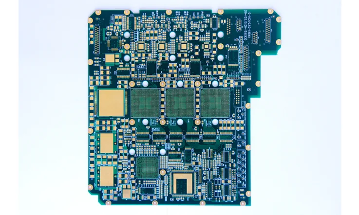
When it comes to high-speed PCB design, having the right tools and technologies at your disposal is like having a well-stocked toolbox—everything you need to get the job done right. Here’s a rundown of some of the must-have tools that can make your design process smoother than a fresh jar of peanut butter.
PCB Design Software
First up, you’ve got your EDA PCB design software. Tools like Altium Designer, Cadence Allegro, and Eagle are the heavy hitters in this arena. They provide features like schematic capture, layout, and simulation, making them essential for creating intricate high-speed designs. Think of these programs as your trusty sidekick—they help you visualize your ideas and catch mistakes before they become a headache.
Having the right design software is crucial for high-speed PCB design. Look for tools that offer:
● Advanced simulation capabilities: These let you analyze designs before you even start manufacturing.
● Built-in design rule checks: These checks catch potential errors early in the design process.
● User-friendly interfaces: Ease of use can significantly enhance productivity.
Simulation Tools
Next on the list are simulation tools. Software like HyperLynx and SPICE helps you run tests on your design virtually, allowing you to predict how it’ll perform in the real world. It’s like having a crystal ball that gives you insight into potential issues, so you can fix them before they rear their ugly heads. The earlier you can catch these problems, the better off you’ll be.
Simulation tools can help predict how your design will behave in real-world conditions. By running simulations, you can catch potential issues before manufacturing, saving you time and money.
Types of Simulations: Look for tools that offer signal integrity analysis, thermal simulations, and power integrity assessments.
Signal Integrity Analysis Tools
Don’t forget about signal integrity analysis tools, either! These tools can analyze your designs to ensure that your signals are clean and strong. Tools like Keysight ADS or ANSYS HFSS are excellent for examining high-frequency behaviors. Using these tools is like putting your design under a microscope, helping you spot any red flags.
Manufacturing Software
Finally, let’s talk about manufacturing software. Tools that handle Gerber file generation and DFM (Design for Manufacturing) checks are crucial in making sure your design can be produced without a hitch. You want to ensure that your design flows smoothly from the digital realm to the physical world, and using the right software helps bridge that gap.
In a words, The right tools can significantly enhance the quality of high-speed designs. Advanced simulation tools and design software allow for detailed analysis and optimization. For example, a tech firm using simulation tools reported a 40% reduction in design errors, leading to faster time-to-market.
Impact of Simulation Tools
| Metric | Without Simulation | With Simulation | Improvement |
| Design Errors | 50 | 30 | 40% reduction |
| Time-to-Market (weeks) | 12 | 8 | 33% faster |
How to Know if You Need a High Speed Design?
Figuring out if you need a high-speed PCB design is like checking your car’s oil before a long trip—it’s all about being prepared. If your device handles high-frequency signals or requires fast data transfers, a high-speed design is definitely in the cards. For instance, if you’re working on anything from telecommunications to high-performance computing, you’ll want to make sure your PCB can keep up with the fast-paced demands without a hitch.
Another telltale sign is the distance your signals need to travel. Longer traces can introduce latency and increase the risk of signal degradation, which is a real buzzkill. If you notice issues like crosstalk or data corruption in your current designs, it’s time to hit the reset button and consider high-speed principles.
| Criteria | Standard Design | High-Speed Design | Benefits |
| Data Transfer Rate | Up to 100 Mbps | Over 100 Mbps | Faster data processing |
| Signal Distance | Longer traces increase risk | Shorter traces minimize risk | Improved signal integrity |
| Applications | Basic consumer devices | Telecommunications, IoT | Enhanced performance |
| Common Issues | Crosstalk, latency | Signal degradation, data loss | Reliable performance under load |
And let’s not forget about the latest tech trends—if you’re gearing up for 5G or IoT, high-speed design is the name of the game. It’s all about staying ahead of the curve and ensuring your products shine in a competitive market.
Difference Between High Speed and High Frequency PCB Design
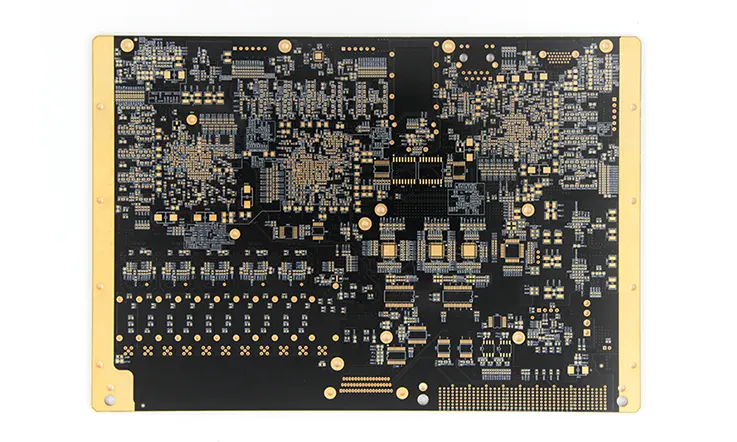
Understanding the difference between high-speed and high-frequency PCB design is like knowing the difference between a sprint and a marathon—both require stamina, but the strategies differ. High-speed PCB design usually refers to boards operating at data rates over 100 Mbps, focusing on maintaining signal integrity and minimizing delay. Techniques such as controlled impedance and short trace lengths come into play here to keep your signals on point.
On the flip side, high-frequency PCB design deals with gigahertz (GHz) signals where things get a bit trickier. This involves considering electromagnetic behavior, such as signal propagation delays and parasitic effects. Key techniques for high-frequency designs include using RF components, careful layer stacking, and materials that minimize dielectric losses.
| Feature | High-Speed PCB Design | High-Frequency PCB Design | Key Differences |
| Operating Frequency | Up to 100 MHz | Gigahertz (GHz) | High-frequency signals behave differently |
| Signal Integrity Focus | Controlled impedance | EM behavior and parasitics | Varies in design approach |
| Design Techniques | Differential pair routing | RF components, layer stacking | Different materials required |
| Performance Metrics | Latency, jitter | Propagation delay, insertion loss | Each has unique performance indicators |
In a nutshell, while all high-frequency designs are inherently high-speed due to their nature, not all high-speed designs operate at high frequencies. Knowing this difference helps you tailor your design strategies and pick the right materials and techniques for your specific needs. It’s about being smart with your design choices so you can hit the ground running.
Applications and Case Studies
High-speed PCBs are making waves across various industries, proving that they’re not just a flash in the pan. Let’s dive into some real-world applications and case studies that showcase how these designs are shaking things up.
Telecommunications
One of the prime applications for high-speed PCB design is in the telecommunications sector. Companies are pushing the envelope to deliver faster internet speeds and more reliable connections. For instance, a major telecom provider implemented high-speed PCB designs in their routers to support 5G networks. By optimizing signal integrity and minimizing latency, they managed to enhance their customers’ experience, proving that a good design can really pack a punch.
Consumer Electronics
High-speed PCBs are also essential in consumer electronics. A well-known electronics manufacturer adopted high-speed PCB designs in their latest devices to support rapid data transfer and enhanced performance. By optimizing these designs, they reduced lag and improved overall responsiveness. Users noticed the difference, leading to rave reviews and skyrocketing sales.
Medical Devices
In the medical field, high-speed PCB designs are saving lives. Medical imaging devices, like MRIs and CT scanners, require precise data processing and fast signal transfer. A recent project demonstrated how a manufacturer upgraded their imaging systems using high-speed PCBs, resulting in quicker processing times and clearer images. This not only improved diagnostic capabilities but also enhanced patient care—talk about a win-win!
Automotive Industry
The automotive sector isn’t left in the dust, either. High-speed PCBs are crucial for advanced driver-assistance systems (ADAS) and electric vehicles (EVs). One notable case involved a leading car manufacturer that integrated high-speed designs into their EVs to improve sensor accuracy and communication between systems. The result? Safer, smarter vehicles that keep drivers and passengers in the loop.
Final Thoughts
High-speed PCB design is an art as much as it is a science. Armed with the right knowledge and tools, you can tackle the complexities of this field and create top-notch designs. Whether you’re an experienced engineer or just starting out, keeping up with the latest techniques and technologies is essential for success.
The journey to mastering high-speed PCB design may seem daunting, but remember that every expert was once a beginner. Embrace the challenges and continuously seek knowledge. Dive into simulations, explore new software, and collaborate with peers.
Ready to take your high-speed PCB designs to the next level? Explore our resources, join our community, and start your journey toward mastering this essential skill today!
Frequently Asked Questions (FAQ)
Q: What’s the best material for high-speed PCBs?
A: Materials like FR-4, Rogers, and polyimide are commonly favored due to their excellent electrical properties.
Q: How do I measure signal integrity?
A: Utilize tools like oscilloscopes and time domain reflectometry (TDR) to assess the quality of signals.
Q: What are some common pitfalls in high-speed PCB design?
A: Common pitfalls include neglecting impedance matching, insufficient thermal management, and poor routing practices.
I am text block. Click edit button to change this text. Lorem ipsum dolor sit amet, consectetur adipiscing elit. Ut elit tellus, luctus nec ullamcorper mattis, pulvinar dapibus leo.

