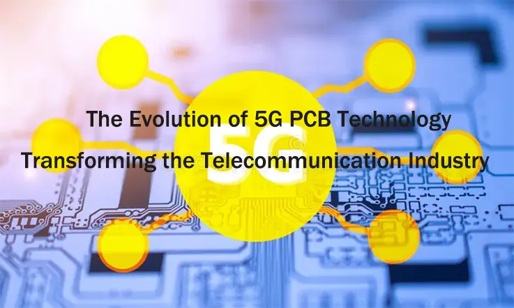
The rapid advancement of telecommunications technology has led to the emergence of 5G, the fifth generation of wireless technology. 5G promises to revolutionize various industries, including healthcare, transportation, manufacturing, and entertainment, by offering significantly faster data transfer speeds, lower latency, and massive device connectivity. However, the successful deployment and operation of 5G networks heavily rely on the underlying infrastructure, particularly the Printed Circuit Board (PCB) industry.
Overview of 5G Technology
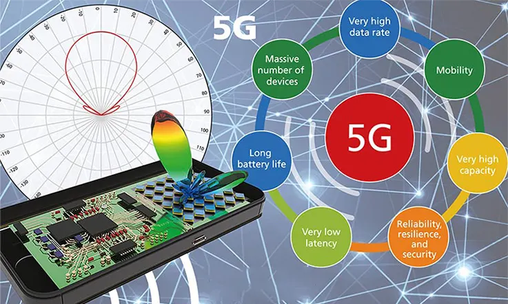
5G, short for the fifth generation of wireless technology, represents a significant leap forward in telecommunications. It is designed to provide faster data speeds, lower latency, increased network capacity, and improved connectivity compared to its predecessor, 4G LTE.
Key Features of 5G
Faster Speeds: 5G offers dramatically faster data transfer speeds compared to previous generations. It has the potential to deliver download speeds of up to 10 gigabits per second (Gbps), enabling ultra-high-definition video streaming, seamless cloud computing, and real-time data-intensive applications.
Lower Latency: Latency refers to the time it takes for data to travel between devices. 5G aims to achieve ultra-low latency, reducing delays to as low as 1 millisecond (ms). This near real-time responsiveness is crucial for applications like autonomous vehicles, remote surgery, and virtual reality gaming.
Increased Capacity: 5G networks can handle a significantly higher number of connected devices simultaneously. This enhanced capacity supports the Internet of Things (IoT) ecosystem, where billions of devices, sensors, and machines are interconnected, enabling smart cities, smart homes, and industrial automation.
Massive Device Connectivity: 5G technology enables massive machine-type communications (mMTC), allowing an enormous number of devices to connect to the network simultaneously. This capability is essential for supporting IoT deployments, where numerous sensors and devices need to transmit data reliably and efficiently.
Network Slicing: 5G introduces the concept of network slicing, which allows the creation of virtual network instances tailored to specific applications or industries. Each network slice can be optimized to meet the unique requirements of diverse use cases, such as autonomous vehicles, smart grids, or augmented reality.
Ultra-Dense Networks: 5G networks rely on a higher density of base stations and smaller cells to provide seamless coverage and capacity. This approach improves network performance in densely populated urban areas and high-traffic locations.
Challenges and Requirements
The deployment of 5G technology comes with various challenges and requirements, including:
Infrastructure Investment: Implementing 5G networks requires substantial investment in infrastructure, including the installation of new base stations, small cells, and fiber-optic networks to support the increased data capacity and coverage.
Spectrum Availability: 5G utilizes a wider range of frequencies, including higher frequency bands known as millimeter waves (mmWave). Ensuring sufficient spectrum availability and managing frequency allocation is crucial for optimal 5G performance.
Compatibility and Interoperability: To maximize the benefits of 5G, devices, applications, and networks need to be compatible and interoperable. This requires industry collaboration and adherence to global standards.
Security and Privacy: With the increased connectivity and data exchange in 5G networks, ensuring robust security measures and protecting user privacy become paramount. Advanced encryption, authentication protocols, and network segmentation are critical in mitigating potential risks.
Regulatory Considerations: Governments and regulatory bodies play a vital role in enabling the deployment of 5G by establishing policies, allocating spectrum, and addressing potential concerns related to health, privacy, and environmental impact.
Therefore, 5G technology represents a transformative leap in wireless communications, offering faster speeds, lower latency, increased capacity, and massive device connectivity. Its deployment requires significant investments in infrastructure, spectrum management, and adherence to security and privacy measures. By addressing these challenges, 5G has the potential to revolutionize various industries, enable innovative applications, and drive the next wave of technological advancements.
4G Vs 5G Technology
4G and 5G are both wireless communication technologies used for mobile networks, but they differ in terms of speed, capacity, latency, and the types of applications they support. Here’s a comparison between 4G and 5G technology:
Speed: 5G offers significantly faster speeds compared to 4G. While 4G can provide download speeds of up to 100 Mbps, 5G can reach peak speeds of several gigabits per second (Gbps). This increased speed enables quicker downloads, smoother streaming, and faster response times.
Capacity: 5G has a much higher capacity than 4G, allowing it to handle a significantly larger number of connected devices simultaneously. This is particularly important in crowded areas with a high concentration of users, such as stadiums or urban environments.
Latency: Latency refers to the time it takes for data to travel between devices. 5G technology has significantly lower latency compared to 4G. While 4G typically has a latency of around 50 milliseconds (ms), 5G can achieve latencies as low as 1 millisecond. This low latency is crucial for applications that require real-time responsiveness, such as autonomous vehicles, remote surgery, and virtual reality.
Spectrum: 4G primarily operates on lower frequency bands, typically below 6 GHz, while 5G utilizes a broader spectrum including both low and high-frequency bands. The use of higher frequency bands (millimeter waves) in 5G allows for faster speeds and greater capacity but has shorter range and can be more easily obstructed by physical objects.
Applications: Both 4G and 5G support voice and data communication, but 5G is designed to cater to a wide range of new applications. With its high speeds, low latency, and increased capacity, 5G enables technologies like autonomous vehicles, smart cities, Internet of Things (IoT) devices, augmented reality (AR), and virtual reality (VR) applications.
Deployment: 4G technology has been widely deployed around the world, providing global coverage. On the other hand, 5G is still in the early stages of deployment, and its coverage varies by region. Initially, 5G networks are being rolled out in urban areas and gradually expanding to suburban and rural regions.
It’s important to note that the benefits of 5G are more pronounced in areas with dense populations and high levels of network congestion. In less populated areas, the advantages of 5G over 4G may be less noticeable.
Overall, 5G technology offers significantly faster speeds, lower latency, increased capacity, and the potential to support a wide range of innovative applications compared to 4G. As 5G continues to deploy and mature, it is expected to revolutionize various industries and enable new technological advancements.
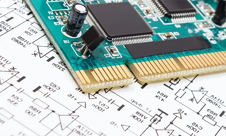
PCB Design Considerations for 5G
Here are some key PCB design considerations for 5G technology:
High-Frequency Design Challenges: 5G operates at significantly higher frequencies compared to previous wireless technologies. PCB designers must carefully consider the impact of high-frequency signals on PCB layout and routing. Factors such as signal integrity, impedance matching, and controlled impedance traces become crucial to minimize signal loss, reflections, and electromagnetic interference.
Miniaturization and Density Requirements: With the increasing complexity of 5G devices and the need for compact form factors, PCB designers must focus on miniaturization and high-density designs. This involves utilizing smaller components, employing advanced packaging techniques such as chip-scale packaging (CSP) and ball grid arrays (BGAs), and optimizing the placement of components and routing of traces to maximize space utilization.
Heat Dissipation and Thermal Management: 5G systems, especially base stations and high-powered devices, generate considerable heat due to increased data transmission rates and power consumption. PCB designers need to incorporate effective thermal management techniques, including heat sinks, thermal vias, and proper PCB layer stackup, to dissipate heat efficiently and prevent overheating, which can affect the performance and reliability of the PCB and the entire 5G system.
Signal Integrity and Transmission Line Considerations: Maintaining signal integrity is critical in 5G PCB designs to ensure accurate and reliable data transmission. PCB designers must pay attention to transmission line characteristics, such as controlled impedance, controlled dielectric constant, and controlled skew, to minimize signal degradation, crosstalk, and electromagnetic interference. Proper routing techniques, such as differential pair routing and microstrip or stripline configurations, are employed to maintain signal integrity.
High-Frequency Material Selection: The choice of PCB materials is crucial in 5G designs to support the high-frequency requirements. PCB designers often opt for specialized materials with low dielectric loss and low dispersion characteristics, such as high-frequency laminates and substrates like PTFE (Polytetrafluoroethylene) or ceramic-filled materials. These materials provide better signal integrity, reduced losses, and improved thermal performance.
Design for Manufacturability (DFM) and Design for Testability (DFT): Considering DFM and DFT principles during the PCB design phase is essential to ensure manufacturability and testability. PCB designers need to collaborate closely with manufacturers to incorporate design elements that facilitate efficient production processes, such as panelization, proper solder mask and stencil design, and component accessibility for testing and inspection.
By addressing these key considerations, PCB designers can create optimized PCB layouts for 5G technology, enabling robust and reliable performance in high-speed, high-frequency, and compact 5G devices and infrastructure.
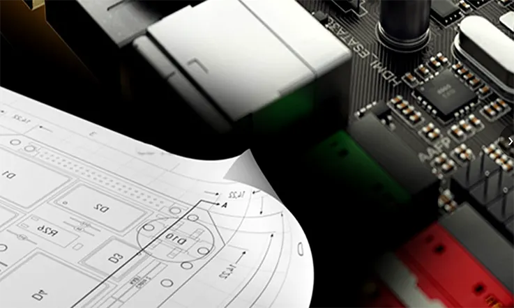
Manufacturing and Testing of 5G PCBs
PCB Manufacturing Process
The manufacturing of 5G PCBs involves several key steps to ensure the production of high-quality and reliable circuit boards. The process typically includes the following stages:
a. Design: The PCB design phase involves creating a layout that accommodates the specific requirements of 5G technology, such as high-frequency signals, miniaturization, and thermal management. Design software and tools are used to create the circuitry, define component placement, and establish signal paths.
b. Material Selection: Choosing the right materials for 5G PCBs is critical. High-frequency laminates with low dielectric loss and controlled impedance characteristics are commonly used. The selection of suitable substrates and copper foils is crucial to ensure signal integrity, thermal dissipation, and mechanical stability.
c. PCB Fabrication: The fabrication process begins with preparing the chosen substrate and applying a conductive layer, typically copper, to create the circuitry. The manufacturing process involves various steps, including drilling, etching, plating, and solder mask application, to create the necessary traces, pads, and vias on the PCB.
d. Component Placement: 5G PCBs often require precise component placement due to the miniaturization and high-density requirements. Automated pick-and-place machines are used to accurately position components on the PCB, ensuring proper electrical connections.
e. Soldering and Assembly: Once the components are placed, the PCB undergoes the soldering process to establish electrical connections between the components and the PCB. Surface mount technology (SMT) is commonly employed for mounting components, and reflow soldering is used to melt solder and create reliable connections.
Quality Control and Testing Procedures
The manufacturing process is accompanied by rigorous quality control and testing procedures to ensure the functionality and reliability of 5G PCBs. The following testing methods are commonly employed:
a. Visual Inspection: Visual inspection is performed to check for any defects, such as soldering issues, misalignment, or damage to the PCB or components. Optical inspection systems and manual inspection are used to identify and rectify any visible issues.
b. Electrical Testing: Electrical testing is conducted to verify the electrical performance of the PCB. This includes tests such as continuity testing, netlist testing, and impedance testing to ensure proper signal transmission and integrity.
c. Functional Testing: Functional testing involves verifying the overall functionality of the 5G PCB in a real-world scenario. This includes testing various features, interfaces, and performance aspects to ensure compliance with specified standards and requirements.
d. Environmental Testing: Environmental testing assesses the PCB’s ability to withstand and operate under different environmental conditions, such as temperature variations, humidity, vibration, and shock. These tests ensure the reliability and durability of 5G PCBs in real-world usage scenarios.
e. Compliance Testing: Compliance testing ensures that the 5G PCB meets industry standards, regulations, and specific requirements set by telecommunications authorities. This includes testing for electromagnetic compatibility (EMC), signal interference, and safety standards.
By adhering to strict manufacturing processes and conducting thorough testing, the PCB industry ensures the production of high-quality, reliable, and performance-driven 5G PCBs. These PCBs form the foundation for the successful implementation of 5G technology, enabling fast and efficient communication in the modern telecommunications landscape.
Role of Printed Circuit Boards (PCBs) in 5G
The role of Printed Circuit Boards (PCBs) in 5G technology is crucial for the successful deployment and operation of advanced wireless networks. PCBs serve as the foundation for connecting and supporting various electronic components within 5G devices and infrastructure. Here are some key roles of PCBs in 5G:
Signal Transmission
PCBs provide the necessary interconnections and transmission paths for high-frequency signals in 5G systems. They enable the efficient transfer of data between components, ensuring reliable and low-latency communication.
Component Integration
PCBs allow for the integration of various components essential for 5G functionality, including microprocessors, integrated circuits, power amplifiers, filters, and antennas. PCBs provide the physical platform for mounting and interconnecting these components, enabling their seamless operation.
Miniaturization and Density
5G devices require smaller, more compact designs to accommodate the increasing number of components and antenna systems. PCBs play a critical role in enabling miniaturization by providing a compact and efficient layout for components, utilizing advanced manufacturing techniques such as multilayer boards and high-density interconnects.
High-Frequency Design
5G operates at higher frequencies compared to previous wireless technologies, such as millimeter-wave frequencies. PCBs designed for 5G must address high-frequency challenges, including impedance control, signal integrity, and minimizing electromagnetic interference (EMI). Specialized PCB materials and design techniques are employed to ensure the reliable transmission of high-frequency signals.
Power Distribution and Management
5G networks require efficient power distribution and management to support the increased power demands of devices and infrastructure. PCBs incorporate power distribution networks (PDNs) to deliver power to various components while minimizing losses and voltage fluctuations. Effective thermal management techniques are also implemented to dissipate heat generated by high-power components.
Reliability and Durability: 5G devices and infrastructure often operate in harsh environments, including extreme temperatures, humidity, and vibration. PCBs must be designed and manufactured to withstand these conditions, ensuring long-term reliability and durability.
Manufacturing and Testing
PCB manufacturers play a critical role in producing high-quality and reliable PCBs for 5G applications. Advanced manufacturing processes, such as automated assembly and inspection, are employed to achieve precise component placement, soldering, and quality control. Rigorous testing procedures, including signal integrity analysis and functional testing, are conducted to ensure the performance and reliability of 5G PCBs.
To sum up, PCBs are integral to the successful implementation of 5G technology. They enable efficient signal transmission, component integration, miniaturization, high-frequency design, power distribution, and reliability. The continuous advancements in PCB technology and manufacturing techniques contribute to the evolution and optimization of 5G devices and infrastructure.
Future Trends and Innovations in 5G PCBs
As 5G technology continues to evolve and expand, the PCB industry is constantly exploring new trends and innovations to meet the ever-growing demands of this transformative technology. Here are some potential future trends and innovations in 5G PCBs:
Advanced Materials and Substrates: The use of advanced materials and substrates is expected to play a crucial role in the development of 5G PCBs. Materials with high thermal conductivity, low signal loss, and improved electrical performance will be sought after to support the higher frequencies and faster data rates of 5G. Innovations in materials like specialized laminates, thin dielectric materials, and metal-core PCBs can enhance signal integrity and thermal management in 5G devices.
Integration of Antennas and RF Components: In 5G systems, the integration of antennas and RF components into PCBs is becoming increasingly important. PCB designers are exploring techniques such as embedded antennas, antenna-in-package (AiP) solutions, and system-on-substrate (SoS) technologies to achieve compact and high-performance designs. Integrating antennas and RF components directly into the PCB can streamline the manufacturing process, improve signal transmission efficiency, and enable smaller form factors for 5G devices.
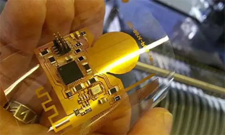
Flex and Rigid-Flex PCBs: Flex and rigid-flex PCBs are expected to gain more prominence in the 5G era. These flexible circuit boards offer unique advantages in terms of space utilization, bendability, and reliability, making them suitable for the compact and intricate designs required by 5G devices. Flex and rigid-flex PCBs can enable the integration of multiple functionalities, reduce the need for connectors, and enhance the durability of devices in 5G applications.
High-Density Interconnects: With the increasing complexity and miniaturization of 5G devices, high-density interconnects (HDIs) will become more prevalent in 5G PCB designs. HDIs allow for more efficient routing of signals, reduced signal interference, and improved electrical performance. Techniques like microvias, blind vias, and stacked vias enable the realization of intricate and compact PCB layouts, accommodating the higher pin counts and tighter component placements of 5G systems.
Signal Integrity and Simulation: With the higher frequencies and faster data rates of 5G, ensuring signal integrity becomes critical. PCB designers will heavily rely on advanced simulation tools and techniques to analyze signal behavior, identify potential issues, and optimize designs for signal integrity. Electromagnetic simulation, impedance control, and crosstalk analysis will be essential for achieving reliable signal transmission and minimizing signal degradation in 5G PCBs.
Packaging and Assembly Techniques: The packaging and assembly of 5G PCBs will witness advancements to meet the demands of high-speed and high-frequency applications. Techniques such as flip-chip bonding, wafer-level packaging, and advanced soldering methods will be explored to achieve precise component placement, reduced signal loss, and improved thermal performance. Innovative packaging solutions can contribute to the miniaturization, power efficiency, and overall performance of 5G devices.
Final Thoughts
The future of 5G PCBs will be shaped by advancements in materials, antenna integration, flex and rigid-flex PCBs, high-density interconnects, signal integrity simulation, and packaging techniques. These innovations will enable the development of smaller, more efficient, and high-performance 5G devices, supporting the widespread adoption and realization of the full potential of 5G technology. The PCB industry will continue to play a crucial role in driving these trends and innovations to meet the evolving demands of the 5G landscape.
Related Posts:
1. Exceptional Manufacturer of Antenna PCBs
2. JarnisTech – High Quality Bluetooth PCB Manufacturer
3. FAQ Guide About Wireless PCB
4. Why Carrier PCB in Telecommunication Is So Useful?